D.Yu. Fedyanin, Surface plasmon polariton amplification upon electrical injection // 2012 E-MRS Spring Meeting
D.Yu. Fedyanin, Surface plasmon polariton amplification upon electrical injection // 2012 E-MRS Spring Meeting, 14-18 May, 2012, Strasbourg, France. (oral presentation)
European Material Research Society YOUNG SCIENTIST AWARD
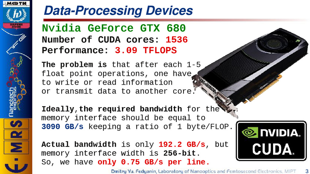
cores: 1536 Performance: 3.09 TFLOPS The problem is that after each 1-5 float point operations, one have to write or read information or transmit data to another core. Ideally,the required bandwidth for the memory interface should be equal to 3090 GB/s keeping a ratio of 1 byte/FLOP. Actual bandwidth is only 192.2 GB/s, but the memory interface width is 256-bit. So, we have only 0.75 GB/s per line.
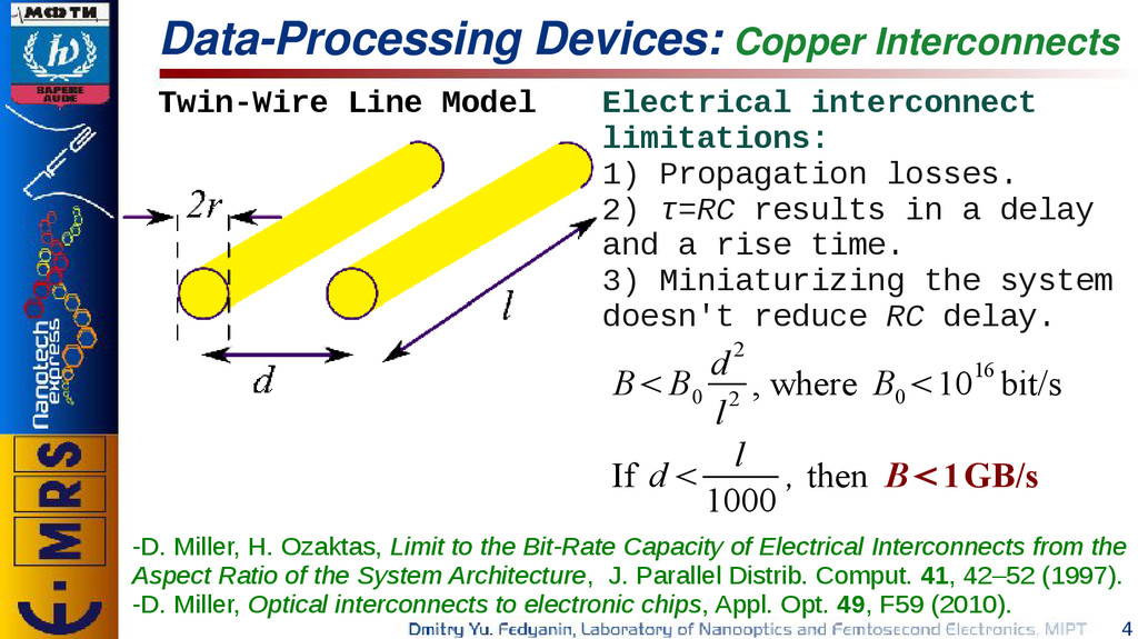
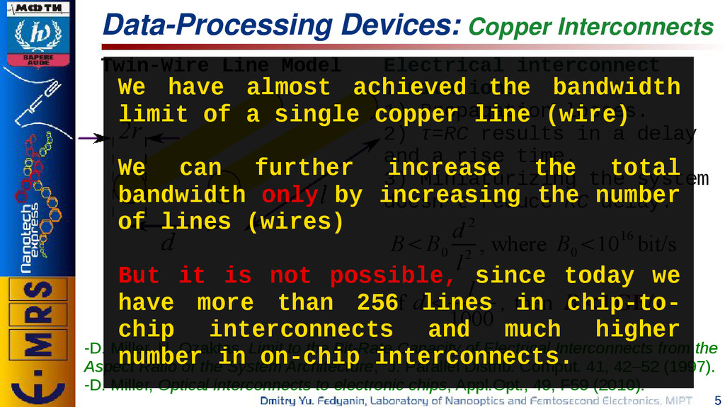
limitations: 1) Propagation losses. 2) τ=RC results in a delay and a rise time. 3) Miniaturizing the system doesn't reduce RC delay. B<B 0 d2 l2 , where B 0 <1016 bit/s If d< l 1000 , then B<1GB/s -D. Miller, H. Ozaktas, Limit to the Bit-Rate Capacity of Electrical Interconnects from the Aspect Ratio of the System Architecture, J. Parallel Distrib. Comput. 41, 42–52 (1997). -D. Miller, Optical interconnects to electronic chips, Appl. Opt. 49, F59 (2010).
2) τ=RC results in a delay and a rise time. 3) Miniaturizing the system doesn't reduce RC delay. B<B 0 d 2 l2 , where B 0 <1016 bit/s If d < l 1000 , then B<1GB/s -D. Miller, H. Ozaktas, Limit to the Bit-Rate Capacity of Electrical Interconnects from the Aspect Ratio of the System Architecture, J. Parallel Distrib. Comput. 41, 42–52 (1997). -D. Miller, Optical interconnects to electronic chips, Appl.Opt., 49, F59 (2010). We have almost achieved the bandwidth limit of a single copper line (wire) We can further increase the total bandwidth only by increasing the number of lines (wires) But it is not possible, since today we have more than 256 lines in chip-to- chip interconnects and much higher number in on-chip interconnects. Data-Processing Devices: Copper Interconnects
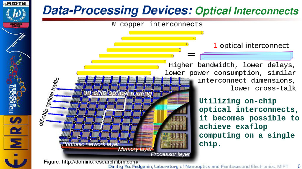
dimensions, lower cross-talk Figure: http://domino.research.ibm.com/ Utilizing on-chip optical interconnects, it becomes possible to achieve exaflop computing on a single chip. Data-Processing Devices: Optical Interconnects
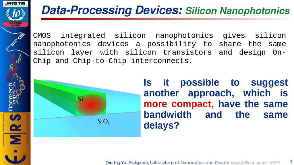
another approach, which is more compact, have the same bandwidth and the same delays? CMOS integrated silicon nanophotonics gives silicon nanophotonics devices a possibility to share the same silicon layer with silicon transistors and design On- Chip and Chip-to-Chip interconnects.
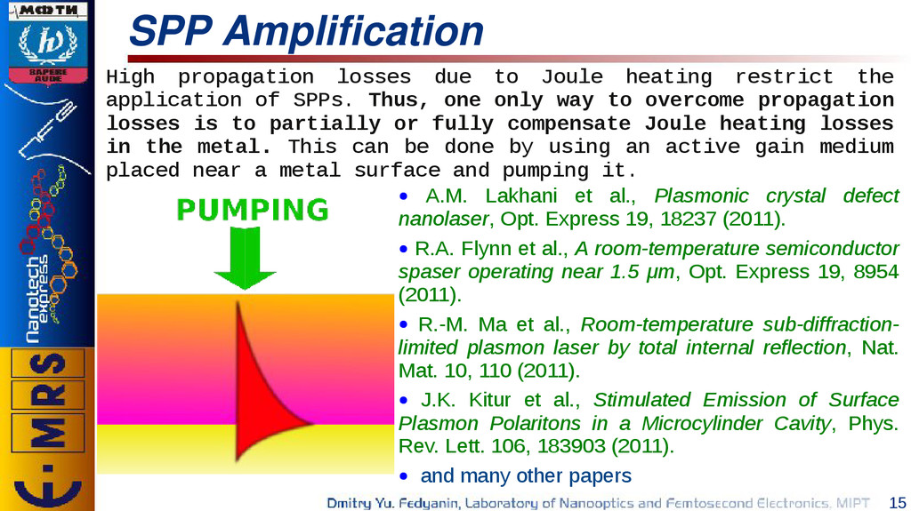
defect nanolaser, Opt. Express 19, 18237 (2011). • R.A. Flynn et al., A room-temperature semiconductor spaser operating near 1.5 μm, Opt. Express 19, 8954 (2011). • R.-M. Ma et al., Room-temperature sub-diffraction- limited plasmon laser by total internal reflection, Nat. Mat. 10, 110 (2011). • J.K. Kitur et al., Stimulated Emission of Surface Plasmon Polaritons in a Microcylinder Cavity, Phys. Rev. Lett. 106, 183903 (2011). • and many other papers High propagation losses due to Joule heating restrict the application of SPPs. Thus, one only way to overcome propagation losses is to partially or fully compensate Joule heating losses in the metal. This can be done by using an active gain medium placed near a metal surface and pumping it.
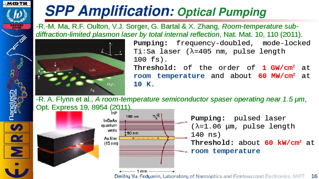
Sorger, G. Bartal & X. Zhang, Room-temperature sub- diffraction-limited plasmon laser by total internal reflection, Nat. Mat. 10, 110 (2011). Pumping: frequency-doubled, mode-locked Ti:Sa laser (λ=405 nm, pulse length 100 fs). Threshold: of the order of 1 GW/cm2 at room temperature and about 60 MW/cm2 at 10 K. -R. A. Flynn et al., A room-temperature semiconductor spaser operating near 1.5 μm, Opt. Express 19, 8954 (2011). Pumping: pulsed laser (λ=1.06 μm, pulse length 140 ns) Threshold: about 60 kW/cm2 at room temperature
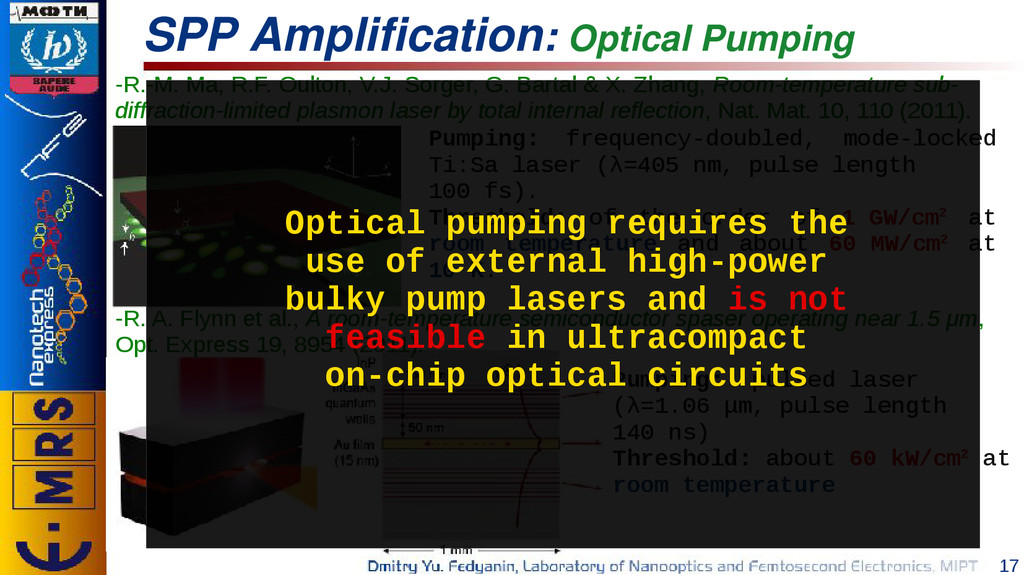
Sorger, G. Bartal & X. Zhang, Room-temperature sub- diffraction-limited plasmon laser by total internal reflection, Nat. Mat. 10, 110 (2011). Pumping: frequency-doubled, mode-locked Ti:Sa laser (λ=405 nm, pulse length 100 fs). Threshold: of the order of 1 GW/cm2 at room temperature and about 60 MW/cm2 at 10 K. -R. A. Flynn et al., A room-temperature semiconductor spaser operating near 1.5 μm, Opt. Express 19, 8954 (2011). Pumping: pulsed laser (λ=1.06 μm, pulse length 140 ns) Threshold: about 60 kW/cm2 at room temperature Optical pumping requires the use of external high-power bulky pump lasers and is not feasible in ultracompact on-chip optical circuits
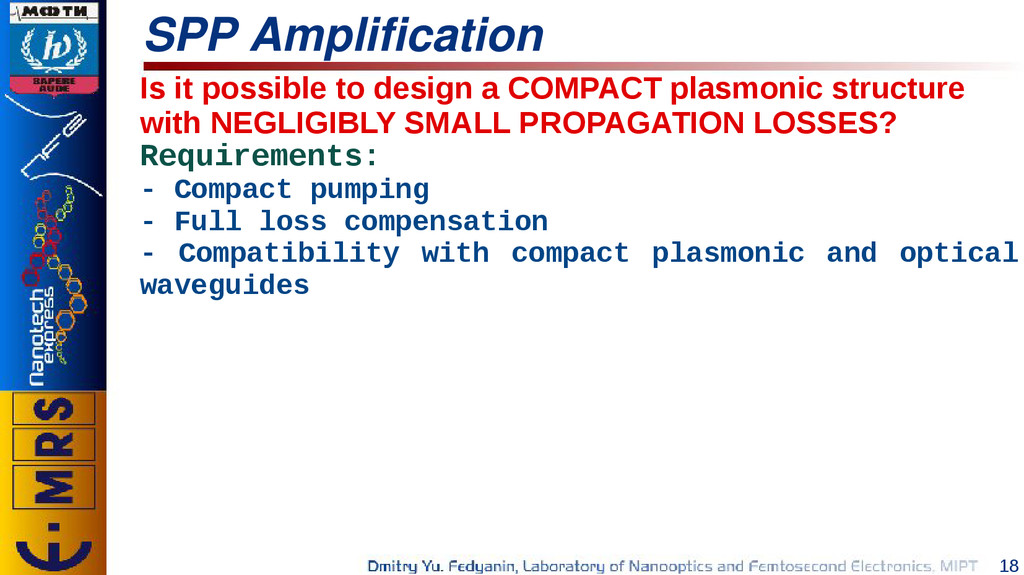
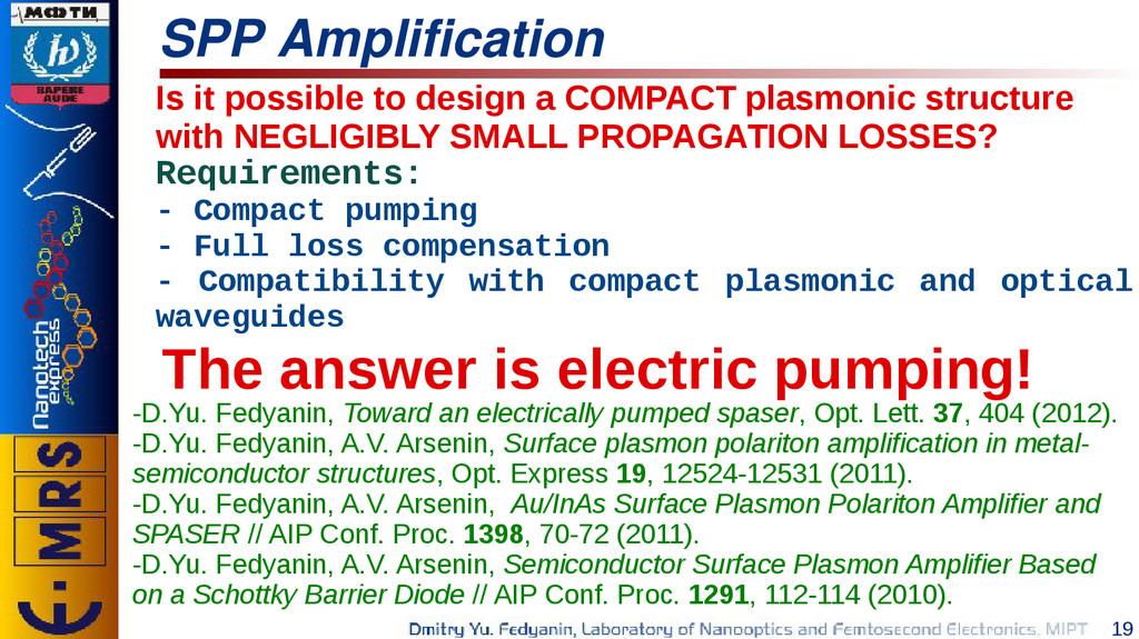
plasmonic structure with NEGLIGIBLY SMALL PROPAGATION LOSSES? Requirements: - Compact pumping - Full loss compensation - Compatibility with compact plasmonic and optical waveguides
Toward an electrically pumped spaser, Opt. Lett. 37, 404 (2012). -D.Yu. Fedyanin, A.V. Arsenin, Surface plasmon polariton amplification in metal- semiconductor structures, Opt. Express 19, 12524-12531 (2011). -D.Yu. Fedyanin, A.V. Arsenin, Au/InAs Surface Plasmon Polariton Amplifier and SPASER // AIP Conf. Proc. 1398, 70-72 (2011). -D.Yu. Fedyanin, A.V. Arsenin, Semiconductor Surface Plasmon Amplifier Based on a Schottky Barrier Diode // AIP Conf. Proc. 1291, 112-114 (2010). Is it possible to design a COMPACT plasmonic structure with NEGLIGIBLY SMALL PROPAGATION LOSSES? Requirements: - Compact pumping - Full loss compensation - Compatibility with compact plasmonic and optical waveguides
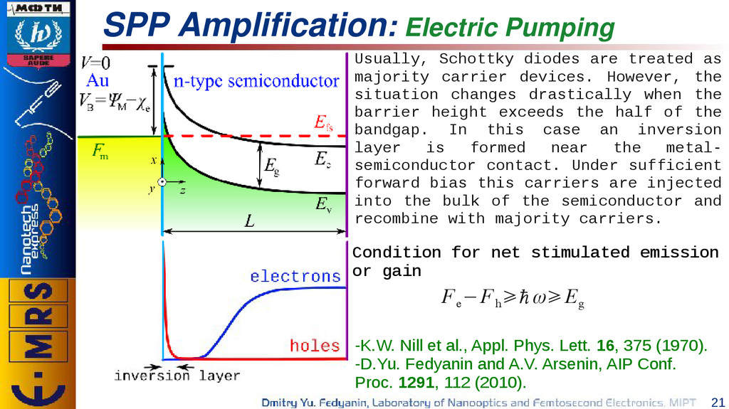
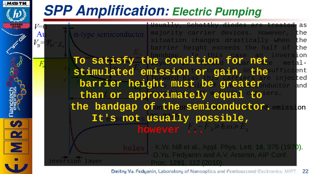
as majority carrier devices. However, the situation changes drastically when the barrier height exceeds the half of the bandgap. In this case an inversion layer is formed near the metal- semiconductor contact. Under sufficient forward bias this carriers are injected into the bulk of the semiconductor and recombine with majority carriers. F e −F h ⩾ℏω⩾E g Condition for net stimulated emission or gain -K.W. Nill et al., Appl. Phys. Lett. 16, 375 (1970). -D.Yu. Fedyanin and A.V. Arsenin, AIP Conf. Proc. 1291, 112 (2010).
as majority carrier devices. However, the situation changes drastically when the barrier height exceeds the half of the bandgap. In this case an inversion layer is formed near the metal- semiconductor contact. Under sufficient forward bias this carriers are injected into the bulk of the semiconductor and recombine with majority carriers. F e −F h ⩾ℏω⩾E g Condition for net stimulated emission or gain - K.W. Nill et al., Appl. Phys. Lett. 16, 375 (1970). -D.Yu. Fedyanin and A.V. Arsenin, AIP Conf. Proc. 1291, 112 (2010). To satisfy the condition for net stimulated emission or gain, the barrier height must be greater than or approximately equal to the bandgap of the semiconductor. It's not usually possible, however ...
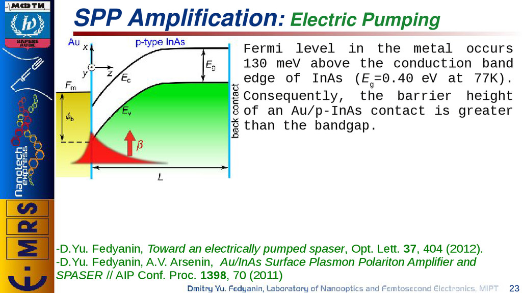
occurs 130 meV above the conduction band edge of InAs (E g =0.40 eV at 77K). Consequently, the barrier height of an Au/p-InAs contact is greater than the bandgap. -D.Yu. Fedyanin, Toward an electrically pumped spaser, Opt. Lett. 37, 404 (2012). -D.Yu. Fedyanin, A.V. Arsenin, Au/InAs Surface Plasmon Polariton Amplifier and SPASER // AIP Conf. Proc. 1398, 70 (2011)
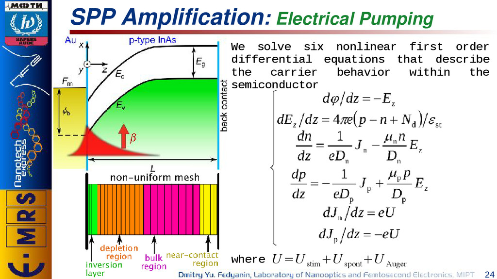
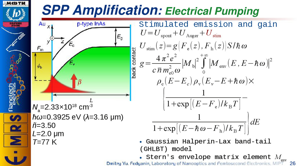
4 π2 e2 c ̄ n m e0 2 ω ∣M b ∣2 ∫ 0 +∞ ∣M env (E , E−ℏω)∣2 ρ c (E−E c ) ρ v (E v −E+ℏω)× { 1 1+exp[(E−F e )/k B T ]− 1 1+exp[(E−ℏω−F h )/k B T ] }dE • Gaussian Halperin-Lax band-tail (GHLBT) model • Stern's envelope matrix element M env U stim (z)=g (F e (z) , F h (z))S /ℏω U =U spont +U Auger +U stim N a =2.33×1018 cm-3 ħω=0.3925 eV (λ=3.16 μm) ñ=3.50 L=2.0 μm T=77 K
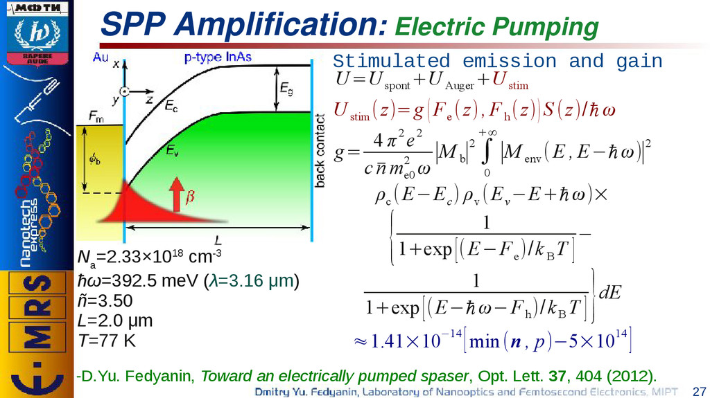
̄ n m e0 2 ω ∣M b ∣2 ∫ 0 +∞ ∣M env (E , E−ℏω)∣2 ρ c (E−E c ) ρ v (E v −E+ℏω)× { 1 1+exp[(E−F e )/k B T ]− 1 1+exp[(E−ℏω−F h )/k B T ] }dE ≈1.41×10⁻¹⁴ [min(n , p)−5×10¹⁴] U stim (z)=g (F e (z), F h (z))S (z)/ℏ ω U =U spont +U Auger +U stim N a =2.33×1018 cm-3 ħω=392.5 meV (λ=3.16 μm) ñ=3.50 L=2.0 μm T=77 K Stimulated emission and gain -D.Yu. Fedyanin, Toward an electrically pumped spaser, Opt. Lett. 37, 404 (2012).
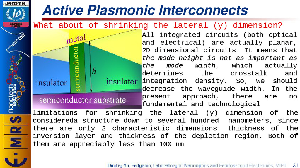
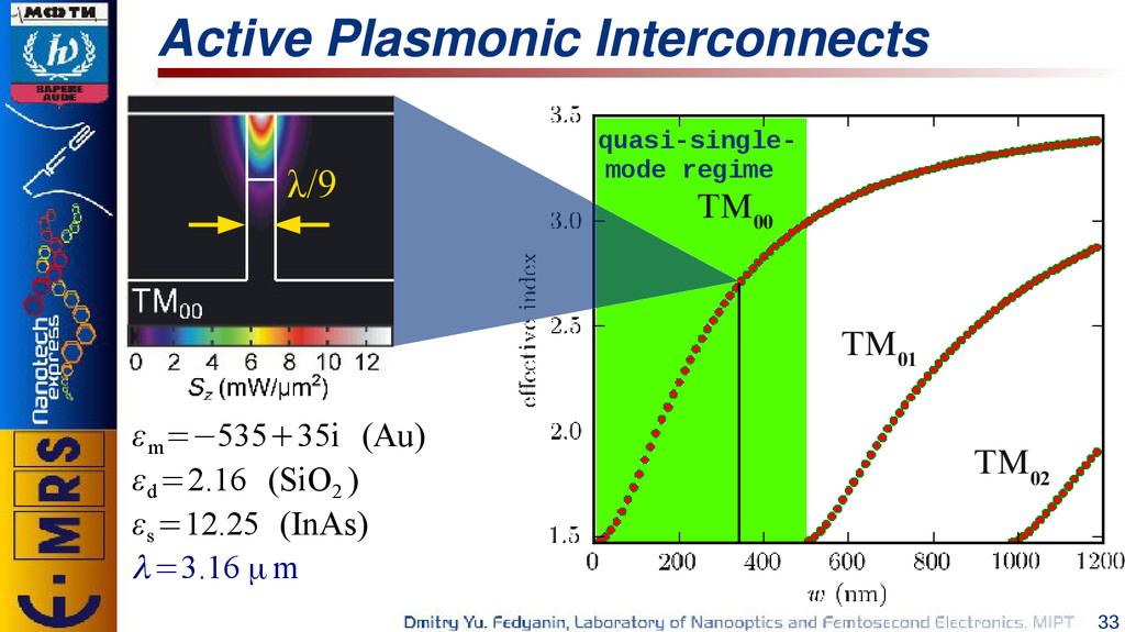
(y) dimension? All integrated circuits (both optical and electrical) are actually planar, 2D dimensional circuits. It means that the mode height is not as important as the mode width, which actually determines the crosstalk and integration density. So, we should decrease the waveguide width. In the present approach, there are no fundamental and technological limitations for shrinking the lateral (y) dimension of the considereda structure down to several hundred nanometers, since there are only 2 characteristic dimensions: thickness of the inversion layer and thickness of the depletion region. Both of them are appreciably less than 100 nm.
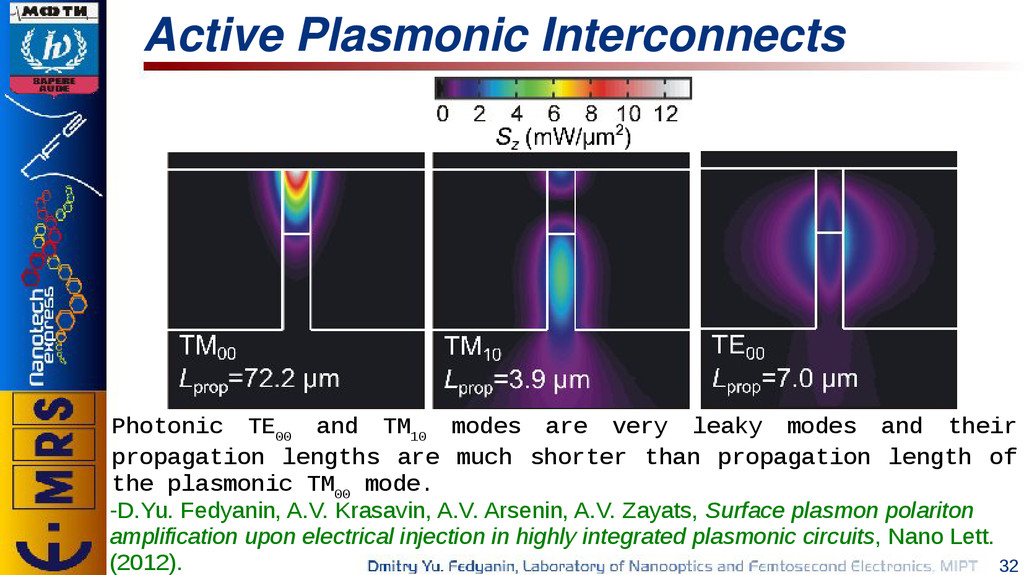
A.V. Zayats, Surface plasmon polariton amplification upon electrical injection in highly integrated plasmonic circuits, Nano Lett. (2012). Photonic TE 00 and TM 10 modes are very leaky modes and their propagation lengths are much shorter than propagation length of the plasmonic TM 00 mode.
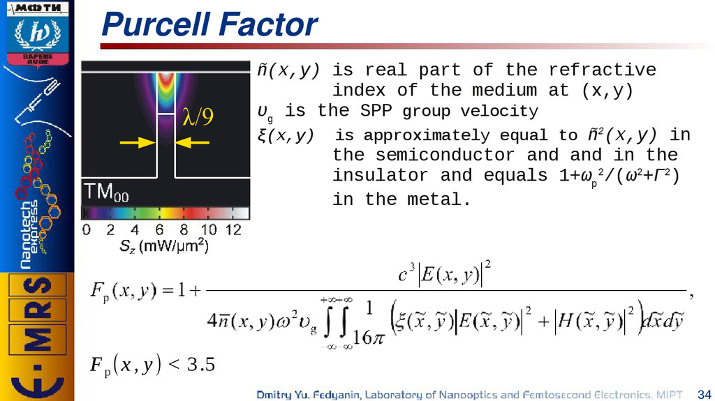
refractive index of the medium at (x,y) υ g is the SPP group velocity ξ(x,y) is approximately equal to ñ2(x,y) in the semiconductor and and in the insulator and equals 1+ω p 2/(ω2+Γ2) in the metal. F p (x , y) < 3.5
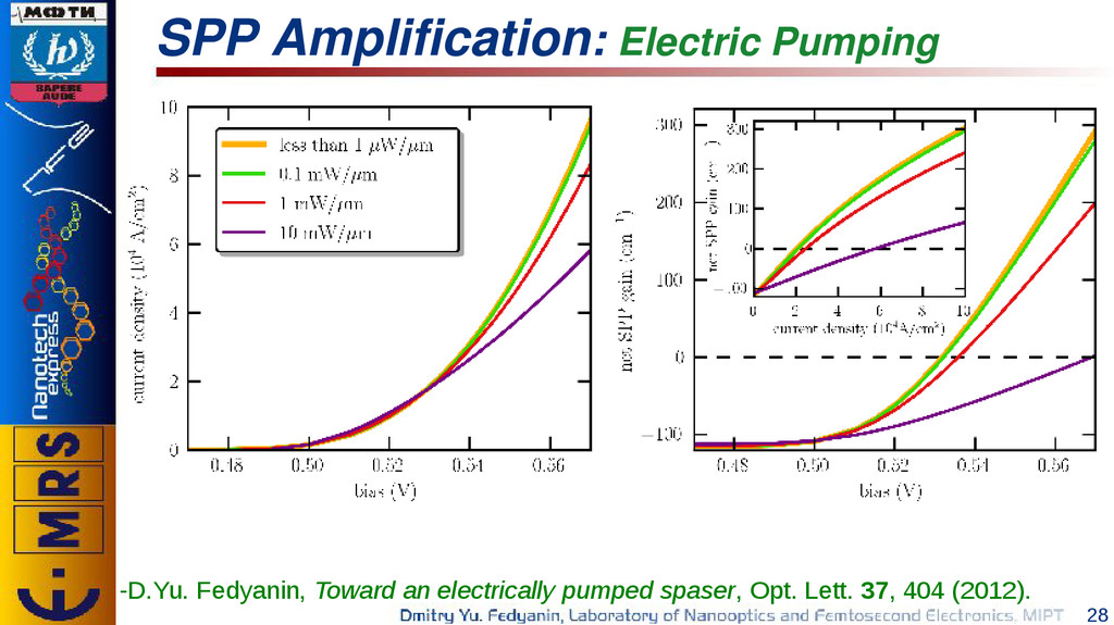
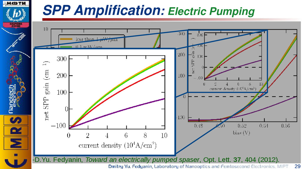
smaller interconnects are achievable with SPP based waveguides, which have the similar bandwidth and delays. • SPP waveguides are quite lossy. However, one can partially or fully compensate losses using an active medium placed near the metal surface. • Optical pumping is very bulky and cannot be used in nanoscale on-chip circuits and we should move to electric pumping. • I've demonstrated an amplification scheme, which is based on a Schottky barrier diode that give a possibility to obtain net SPP gain. • The obtained values of the threshold current are relatively small to design pulsed and even a cw SPP amplifiers and active plasmonic waveguides. • There are no physical limitations for shrinking the lateral dimension of the proposed structure down to deep-subwavelength scale and development of on-chip plasmonic interconnects.
![E-mail: [email protected] Web: http://nano.phystech.edu Thank you for your attention!](https://files.speakerdeck.com/presentations/cf546ad09c950131cbac526b40603ada/slide_35.jpg)