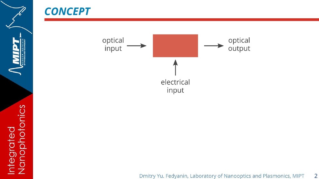
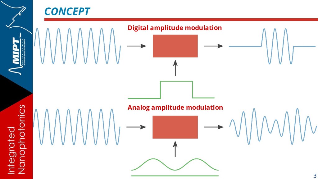
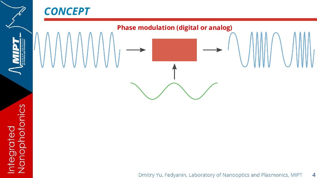
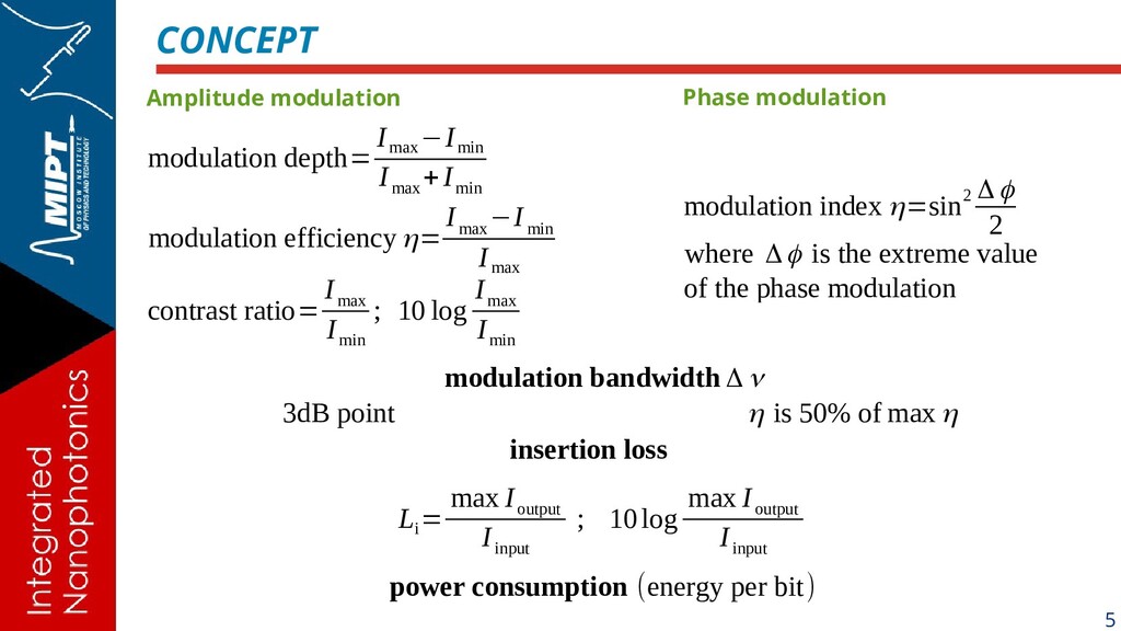
+I min modulation efficiency η= I max −I min I max contrast ratio= I max I min ; 10 log I max I min modulation bandwidth Δ ν modulation index η=sin2 Δ ϕ 2 where Δ ϕ is the extreme value of the phase modulation Phase modulation Amplitude modulation 3dB point η is 50% of max η insertion loss L i = max I output I input ; 10log max I output I input power consumption (energy per bit)
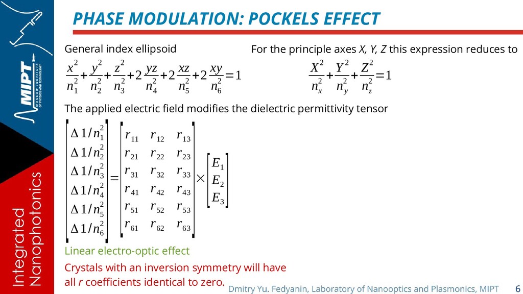
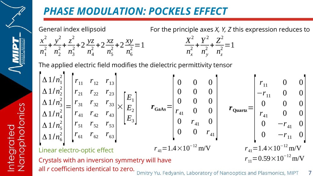
y2 n 2 2 + z2 n 3 2 +2 yz n 4 2 +2 xz n 5 2 +2 xy n 6 2 =1 Linear electro-optic effect General index ellipsoid For the principle axes X, Y, Z this expression reduces to X2 n x 2 + Y2 n y 2 + Z2 n z 2 =1 The applied electric field modifies the dielectric permittivity tensor [Δ 1/n 1 2 Δ 1/n 2 2 Δ 1/n 3 2 Δ1/n 4 2 Δ 1/n 5 2 Δ1/n 6 2 ]= [r 11 r 12 r 13 r 21 r 22 r 23 r 31 r 32 r 33 r 41 r 42 r 43 r 51 r 52 r 53 r 61 r 62 r 63 ]× [E 1 E 2 E 3 ] Crystals with an inversion symmetry will have all r coefficients identical to zero.
y2 n 2 2 + z2 n 3 2 +2 yz n 4 2 +2 xz n 5 2 +2 xy n 6 2 =1 Linear electro-optic effect General index ellipsoid For the principle axes X, Y, Z this expression reduces to X2 n x 2 + Y2 n y 2 + Z2 n z 2 =1 The applied electric field modifies the dielectric permittivity tensor [Δ 1/n 1 2 Δ 1/n 2 2 Δ 1/n 3 2 Δ1/n 4 2 Δ 1/n 5 2 Δ1/n 6 2 ]= [r 11 r 12 r 13 r 21 r 22 r 23 r 31 r 32 r 33 r 41 r 42 r 43 r 51 r 52 r 53 r 61 r 62 r 63 ]× [E 1 E 2 E 3 ] Crystals with an inversion symmetry will have all r coefficients identical to zero. r GaAs = [0 0 0 0 0 0 0 0 0 r 41 0 0 0 r 41 0 0 0 r 41 ] r Quartz = [r 11 0 0 −r 11 0 0 0 0 0 r 41 0 0 0 −r 41 0 0 −r 11 0 ] r 41 =1.4×10⁻¹² m/V r 41 =1.4×10⁻¹² m/V r 11 =0.59×10⁻¹² m/V
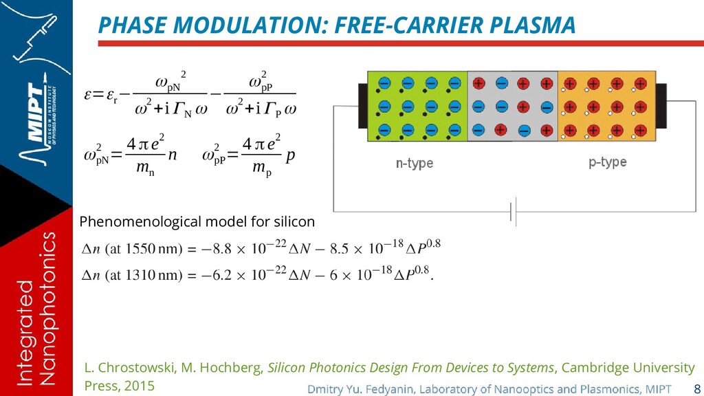
+iΓN ω − ωpP 2 ω2 +iΓP ω ωpN 2 = 4 πe2 m n n ωpP 2 = 4 πe2 m p p Phenomenological model for silicon L. Chrostowski, M. Hochberg, Silicon Photonics Design From Devices to Systems, Cambridge University Press, 2015
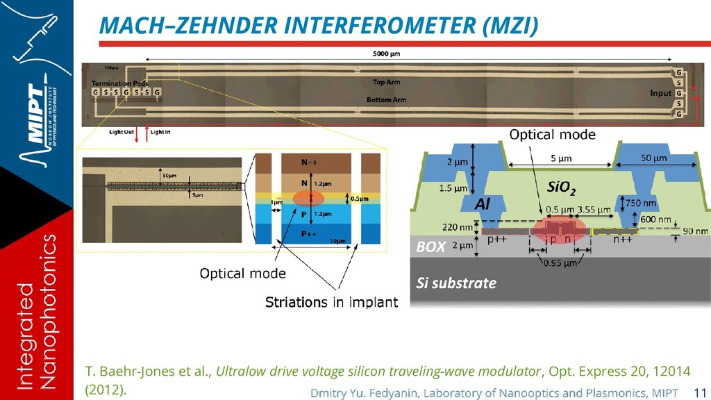
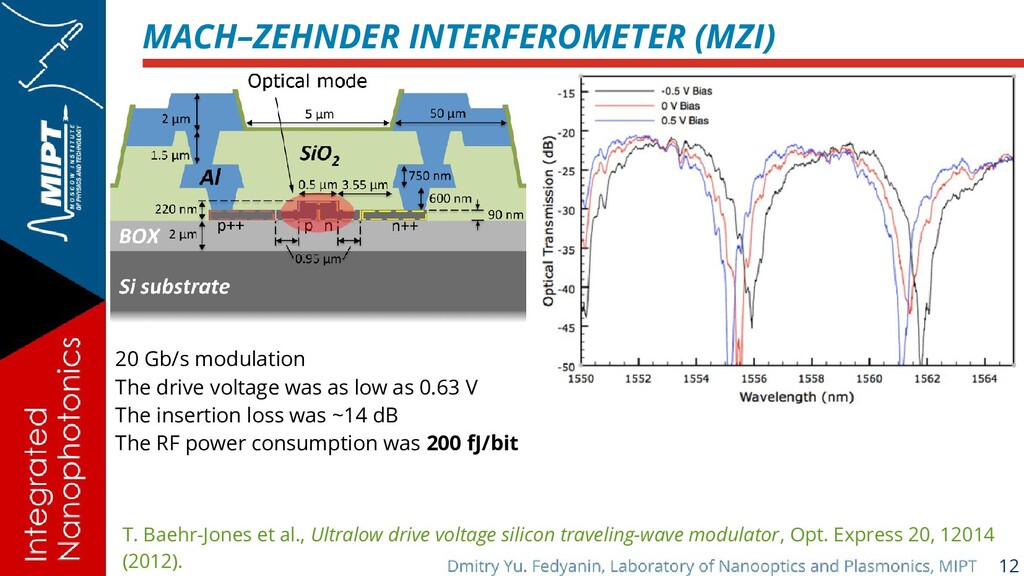
voltage silicon traveling-wave modulator, Opt. Express 20, 12014 (2012). 20 Gb/s modulation The drive voltage was as low as 0.63 V The insertion loss was ~14 dB The RF power consumption was 200 fJ/bit
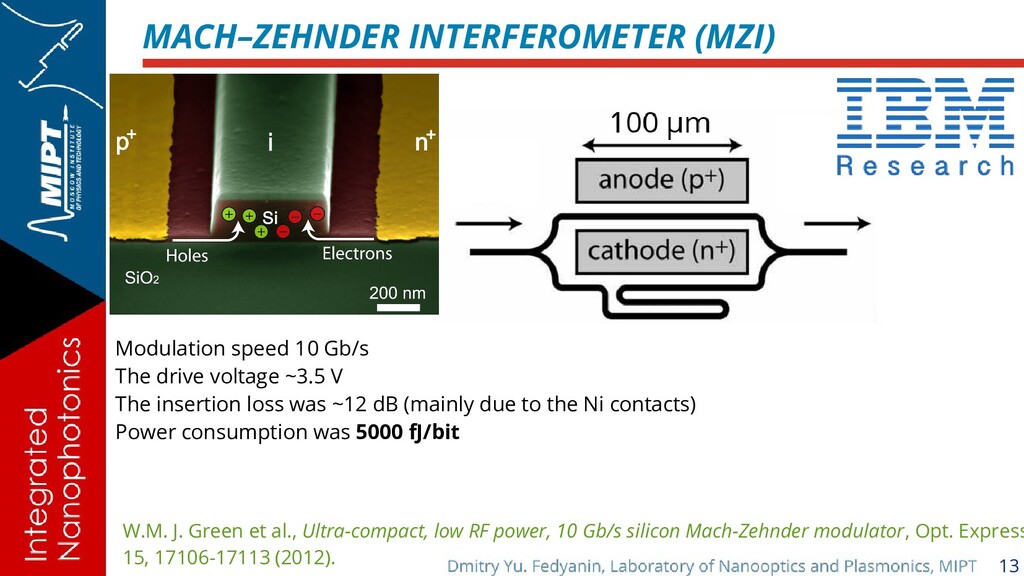
low RF power, 10 Gb/s silicon Mach-Zehnder modulator, Opt. Express 15, 17106-17113 (2012). Modulation speed 10 Gb/s The drive voltage ~3.5 V The insertion loss was ~12 dB (mainly due to the Ni contacts) Power consumption was 5000 fJ/bit
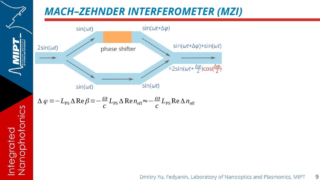
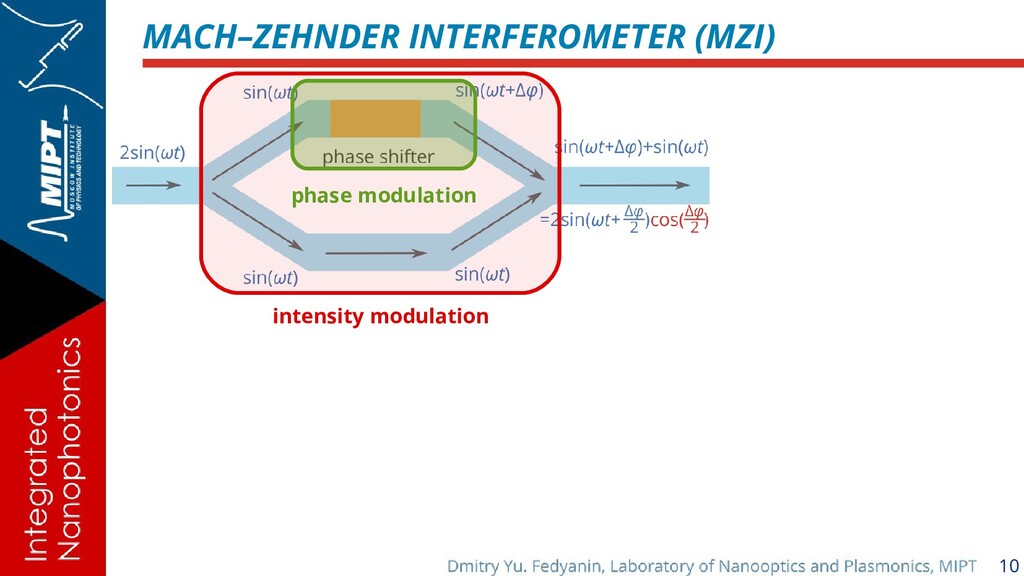
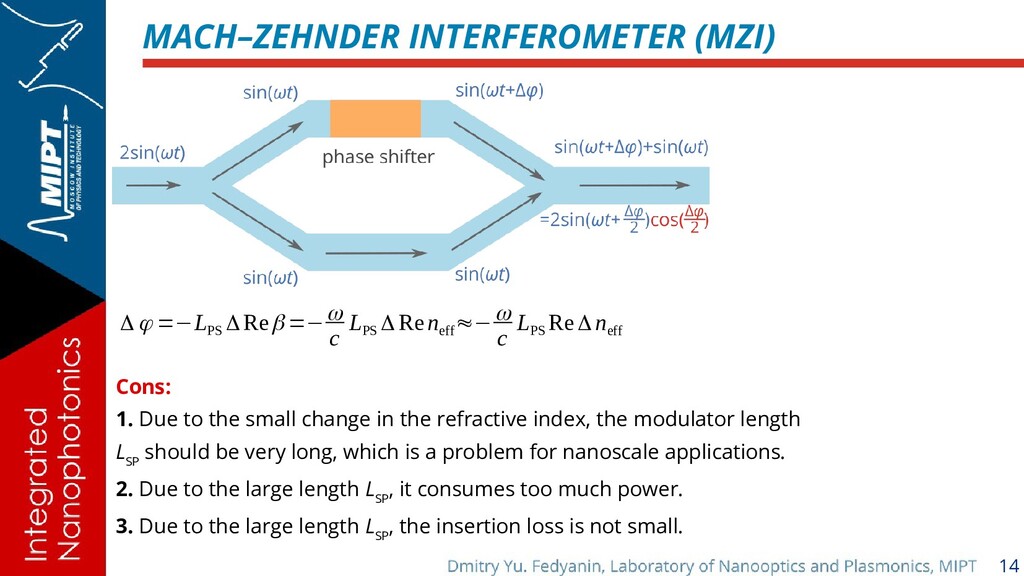
=−ω c L PS Δ Ren eff ≈−ω c L PS ReΔ n eff Cons: 1. Due to the small change in the refractive index, the modulator length L SP should be very long, which is a problem for nanoscale applications. 2. Due to the large length L SP , it consumes too much power. 3. Due to the large length L SP , the insertion loss is not small.
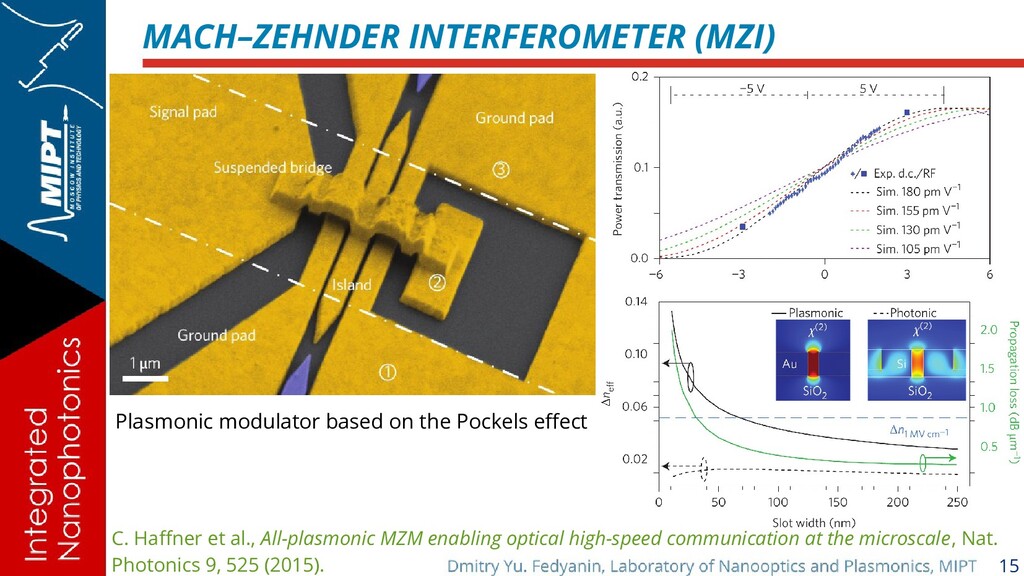
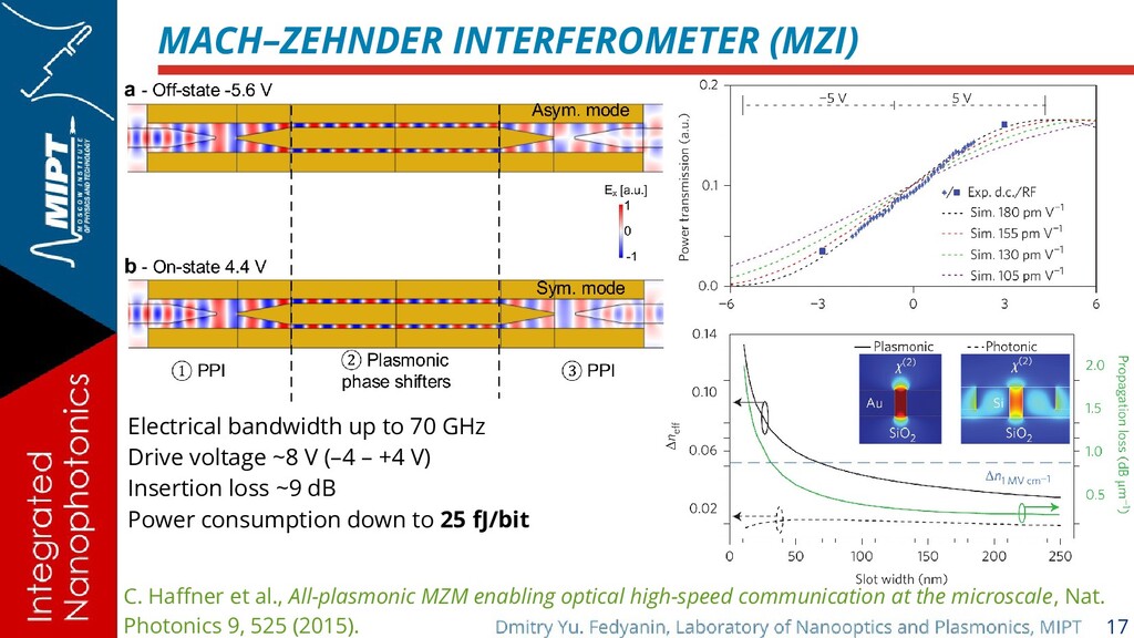
enabling optical high-speed communication at the microscale, Nat. Photonics 9, 525 (2015). Electrical bandwidth up to 70 GHz Drive voltage ~8 V (–4 – +4 V) Insertion loss ~9 dB Power consumption down to 25 fJ/bit
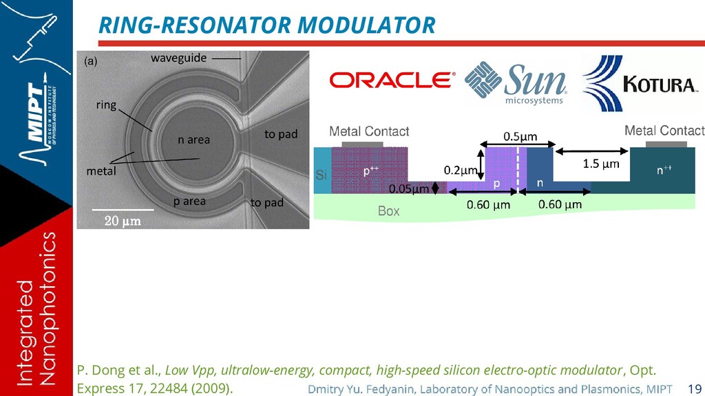
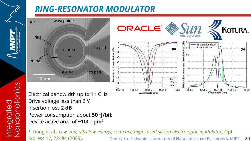
compact, high-speed silicon electro-optic modulator, Opt. Express 17, 22484 (2009). Electrical bandwidth up to 11 GHz Drive voltage less than 2 V Insertion loss 2 dB Power consumption about 50 fJ/bit Device active area of ~1000 μm2
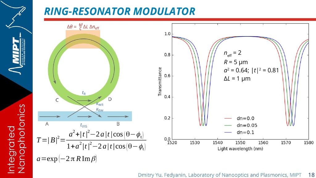
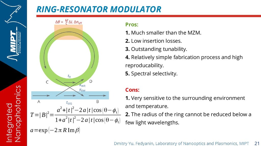
) 1+a2 |t |2 −2a|t |cos(θ−ϕt ) a=exp(−2 π R Imβ) Pros: 1. Much smaller than the MZM. 2. Low insertion losses. 3. Outstanding tunability. 4. Relatively simple fabrication process and high reproducability. 5. Spectral selectivity. Cons: 1. Very sensitive to the surrounding environment and temperature. 2. The radius of the ring cannot be reduced below a few light wavelengths.
)L] Insertion loss L i =exp[−2 ω c Imn eff | V =0 L] Modulation efficiency η=1−exp[−2 ω c (Imn eff | V =V d −Imn eff | V =0 ) L] =1−exp[−2ω c ImΔ n eff L] Pros: 1. Very small size. 2. High robustness: poor sensitivity to the surrounding environment and temperature. 3. Broadband spectral operation. Cons: 1. The insertion loss is higher than that of the ring-resonator modulator. 2. No spectral selectivity and tunability.
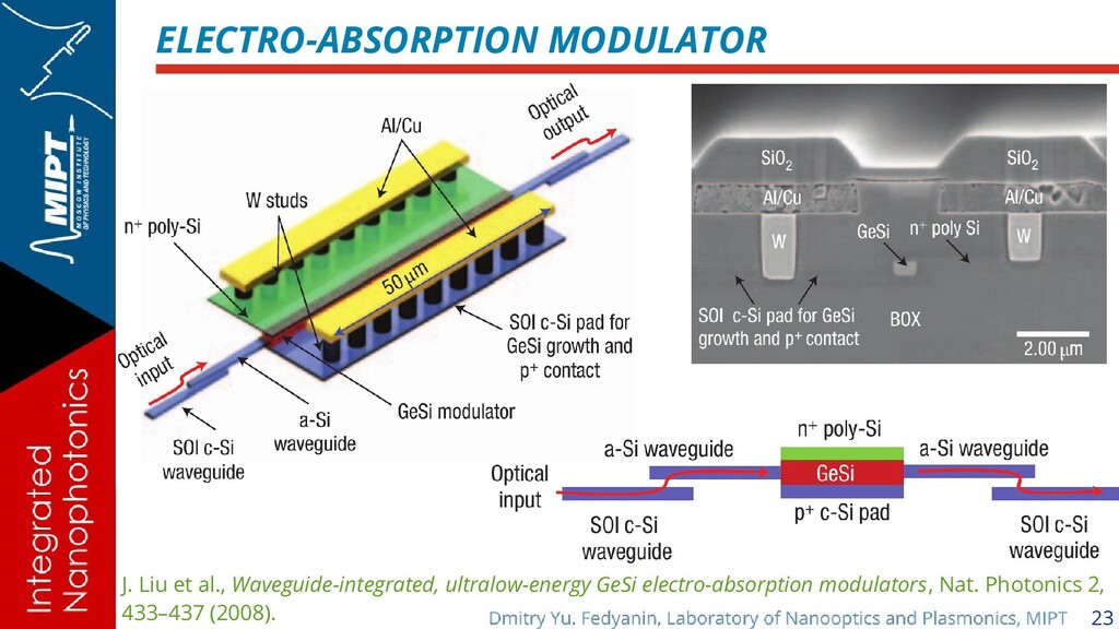
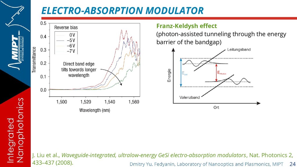
electro-absorption modulators, Nat. Photonics 2, 433–437 (2008). Franz-Keldysh effect (photon-assisted tunneling through the energy barrier of the bandgap)
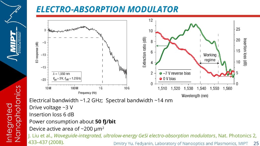
nm Drive voltage ~3 V Insertion loss 6 dB Power consumption about 50 fJ/bit Device active area of ~200 μm2 J. Liu et al., Waveguide-integrated, ultralow-energy GeSi electro-absorption modulators, Nat. Photonics 2, 433–437 (2008).
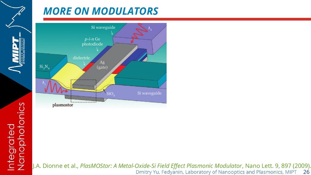
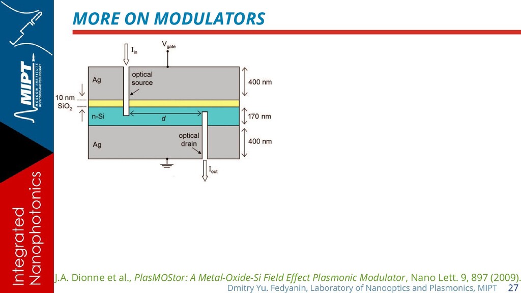
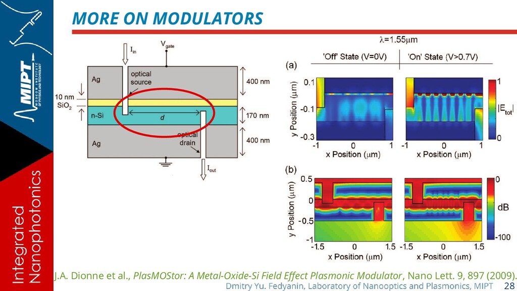
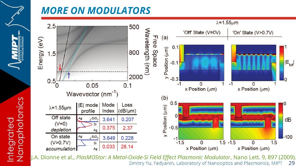
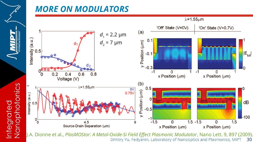
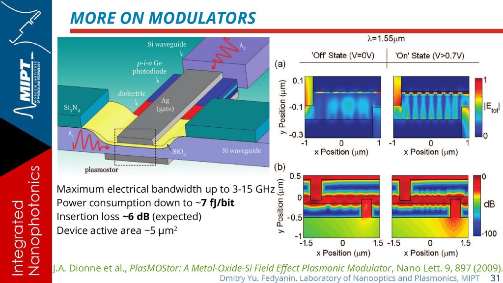
Metal-Oxide-Si Field Effect Plasmonic Modulator, Nano Lett. 9, 897 (2009). Maximum electrical bandwidth up to 3-15 GHz Power consumption down to ~7 fJ/bit Insertion loss ~6 dB (expected) Device active area ~5 μm2
![22 ELECTRO-ABSORPTION MODULATOR T=exp[−2Imβ(V )L]=exp[−2 ω c Imn eff (V](https://files.speakerdeck.com/presentations/f90baa182a644c249e0586973374f1cd/slide_21.jpg)