Yadrav (Ichalkaranji)-416121, Dist. – Kolhapur (Approved by AICTE, New Delhi, Recognized by Government of Maharashtra & Affiliated to BATU University, Lonere) NBA Accredited Programs, Accredited By NAAC ‘A’ Grade,ISO 9001:2015 Certified Electronics & Computer Engineering Department
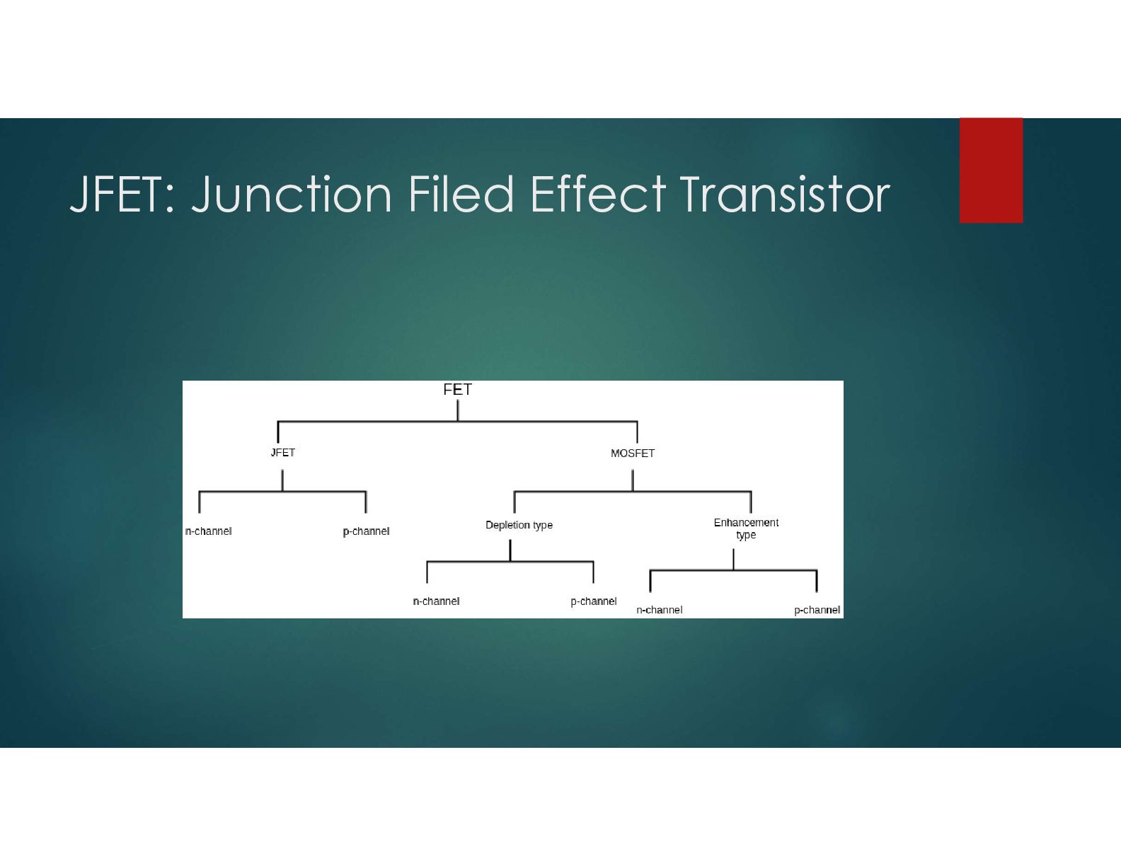
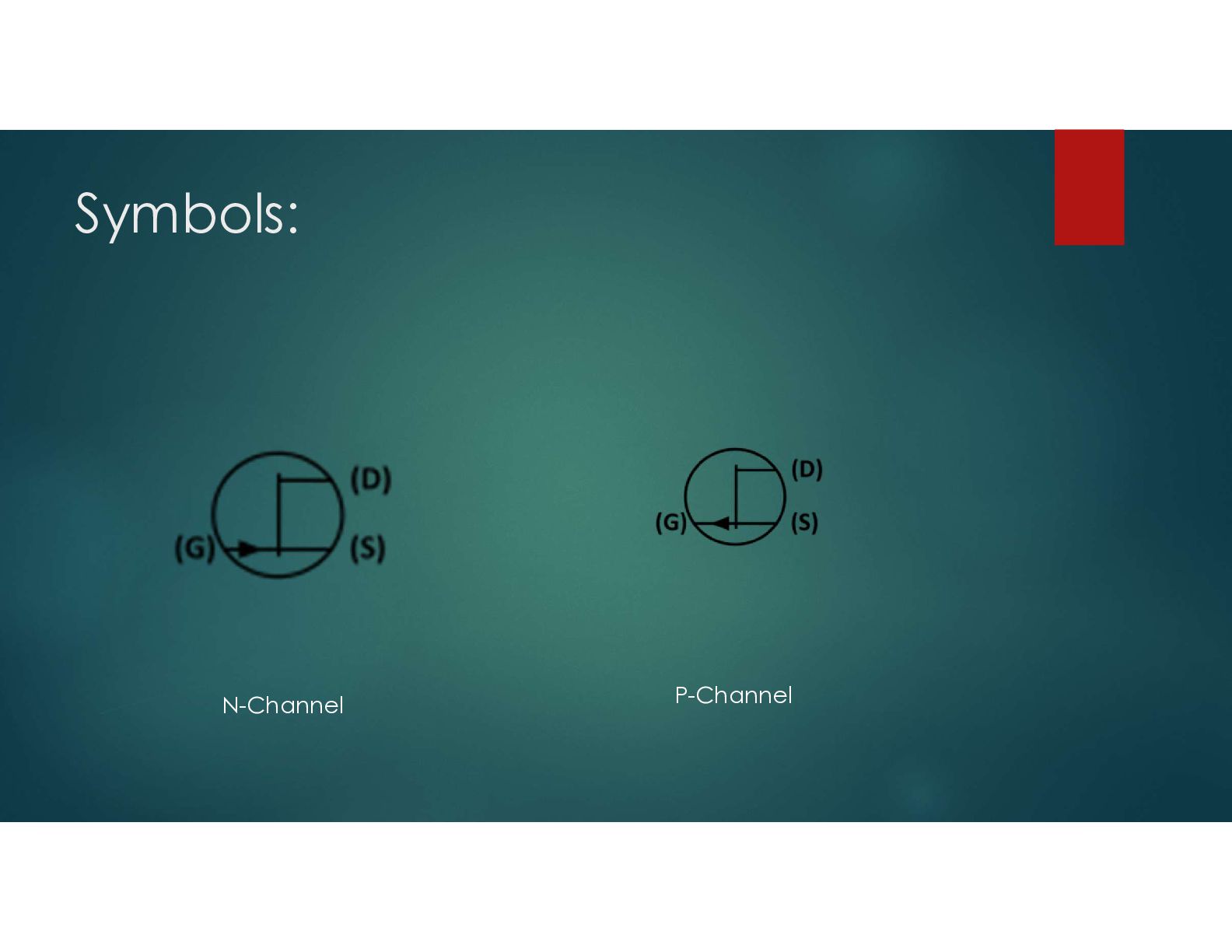
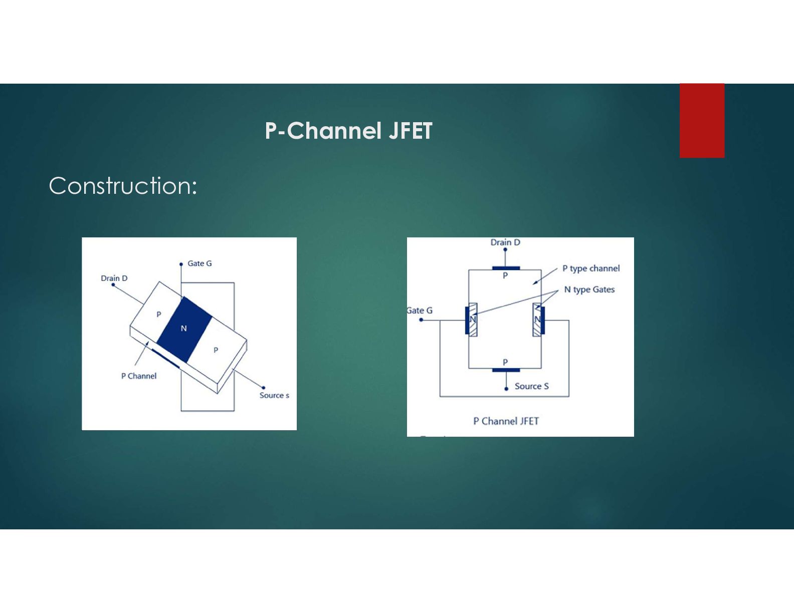
enter), Drain (where carriers exit), and Gate (the control input). •N-Channel: Uses electrons for conduction; features higher conductivity and mobility than p-channel types. •P-Channel: Uses holes for conduction; requires reversed voltage polarities compared to n-channel
temperature variations, which allows them to adapt their properties with changing temperatures. In certain applications, proper thermal management may be necessary. •Low Noise: JFETs are known for their low noise, which is valuable in applications such as amplifier and sensors where signal integrity is essential. •High input impedance: The high input impedance of JFETs remains relatively stable over a range of temperatures and voltages, making them suitable fo •r precision applications. •Variants: JFETs, which allow circuit design flexibility and enable applications that require both sourcing and sinking current, are available in two types of channels: N channel and P Channel.
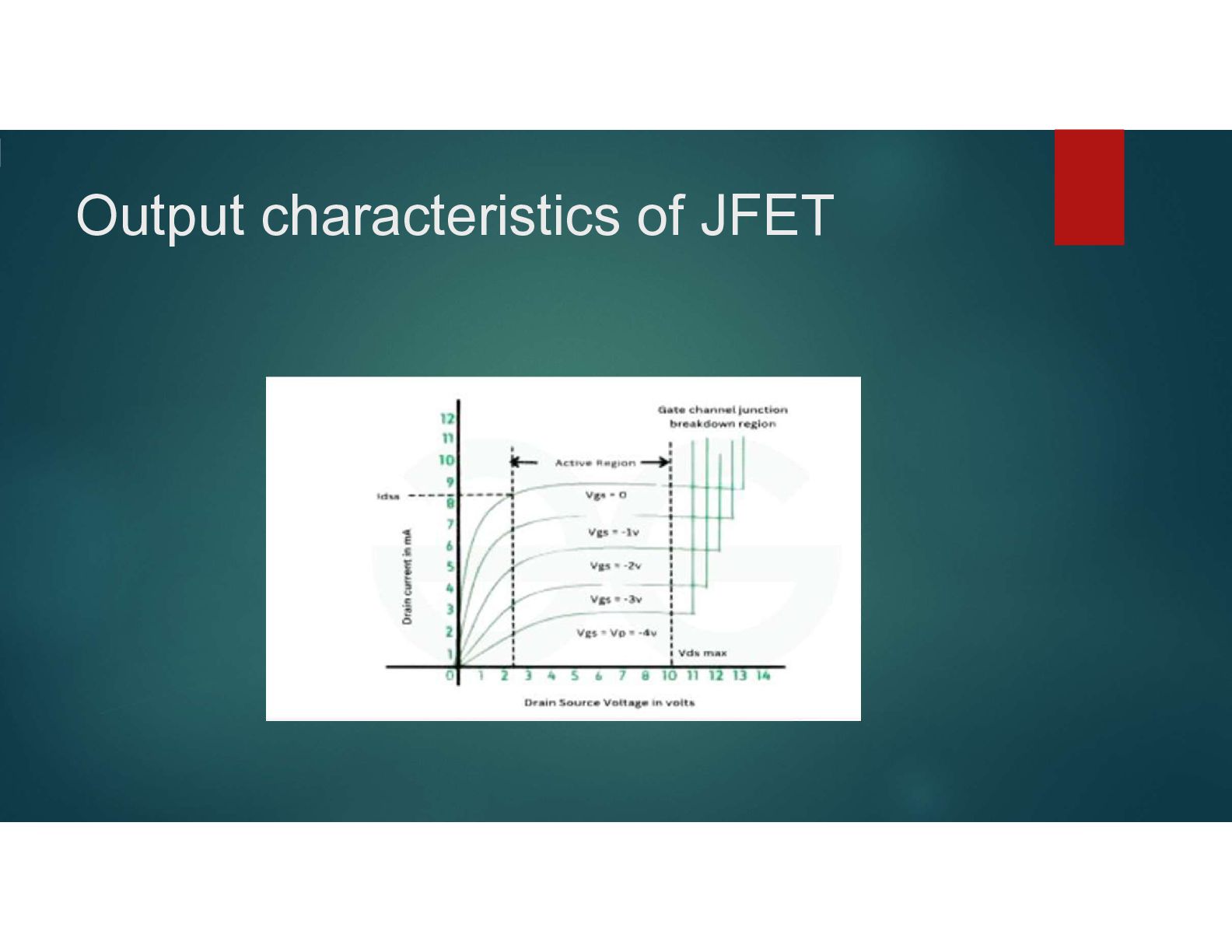
JFET: •Saturation region: In this region, the JFET operates with low Vds, and the current is constant. The current is controlled by the gate source voltage (V ). gs •Ohmic region: JFET becomes an ohmic region with increasing VDS. The drain current increases with Vds. •Pinched off region: By increasing the VDS, it can lead to a pinch of region; in this region, the channel narrows and the drain current becomes independent of the VDS. •Breakdown Region: As the voltage of drain source becomes very high then the JFET channels gets breakdown and current flows in an uncontrolled manner.


 ammeep
 jnunemaker
 irinanazarova
 leimatthew05
 jonrohan
 rmw
 kneath
 reverentgeek
 inesmontani
 bethany
 akademiya2063
 tammielis