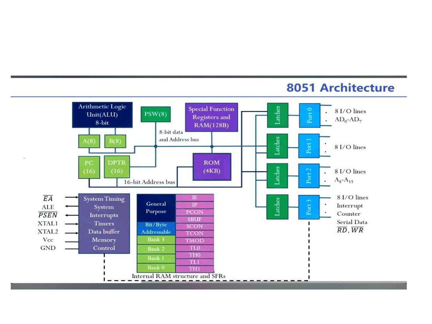
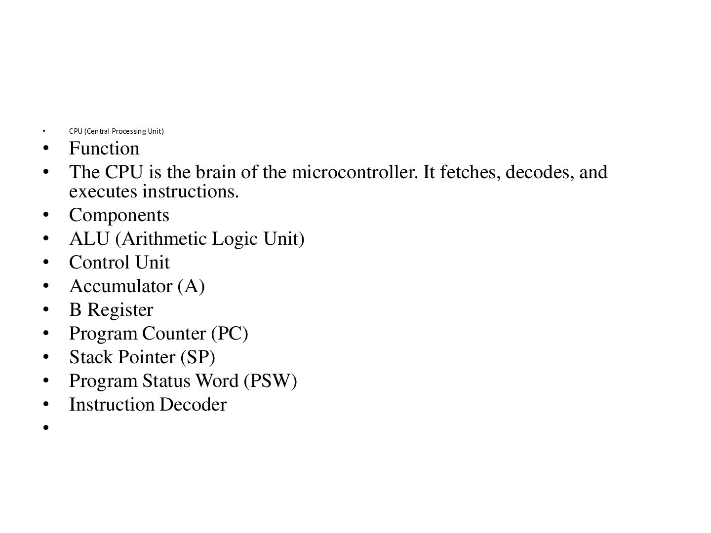
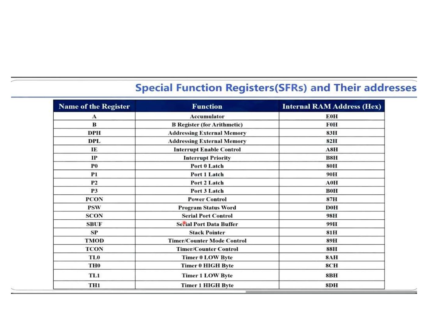
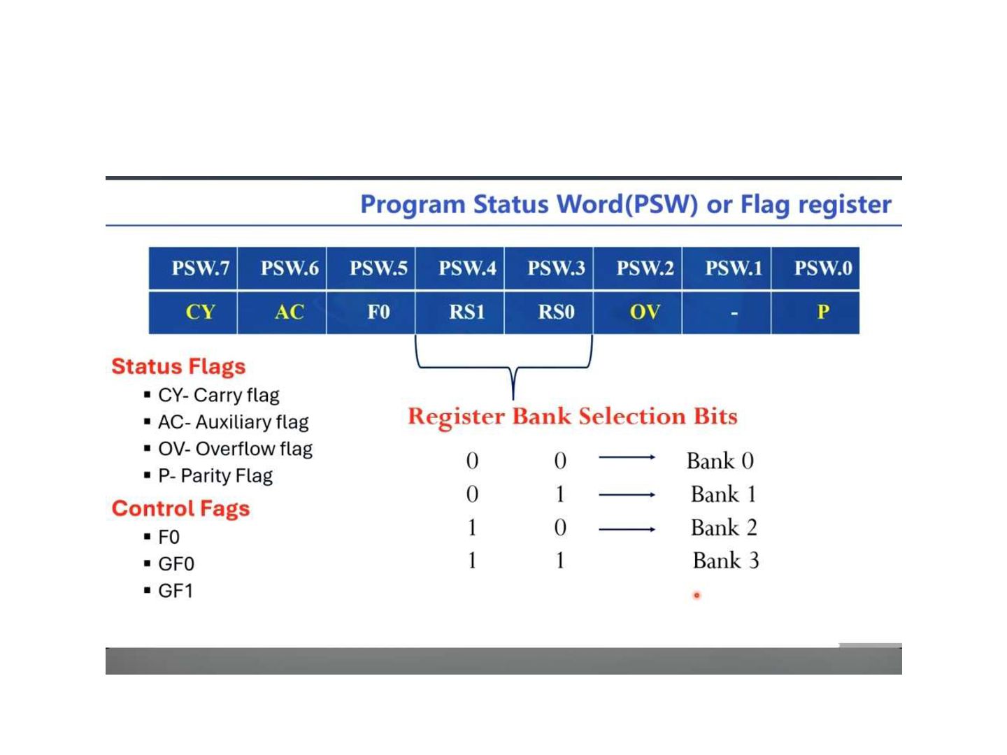
is the brain of the microcontroller. It fetches, decodes, and executes instructions. • Components • ALU (Arithmetic Logic Unit) • Control Unit • Accumulator (A) • B Register • Program Counter (PC) • Stack Pointer (SP) • Program Status Word (PSW) • Instruction Decoder •
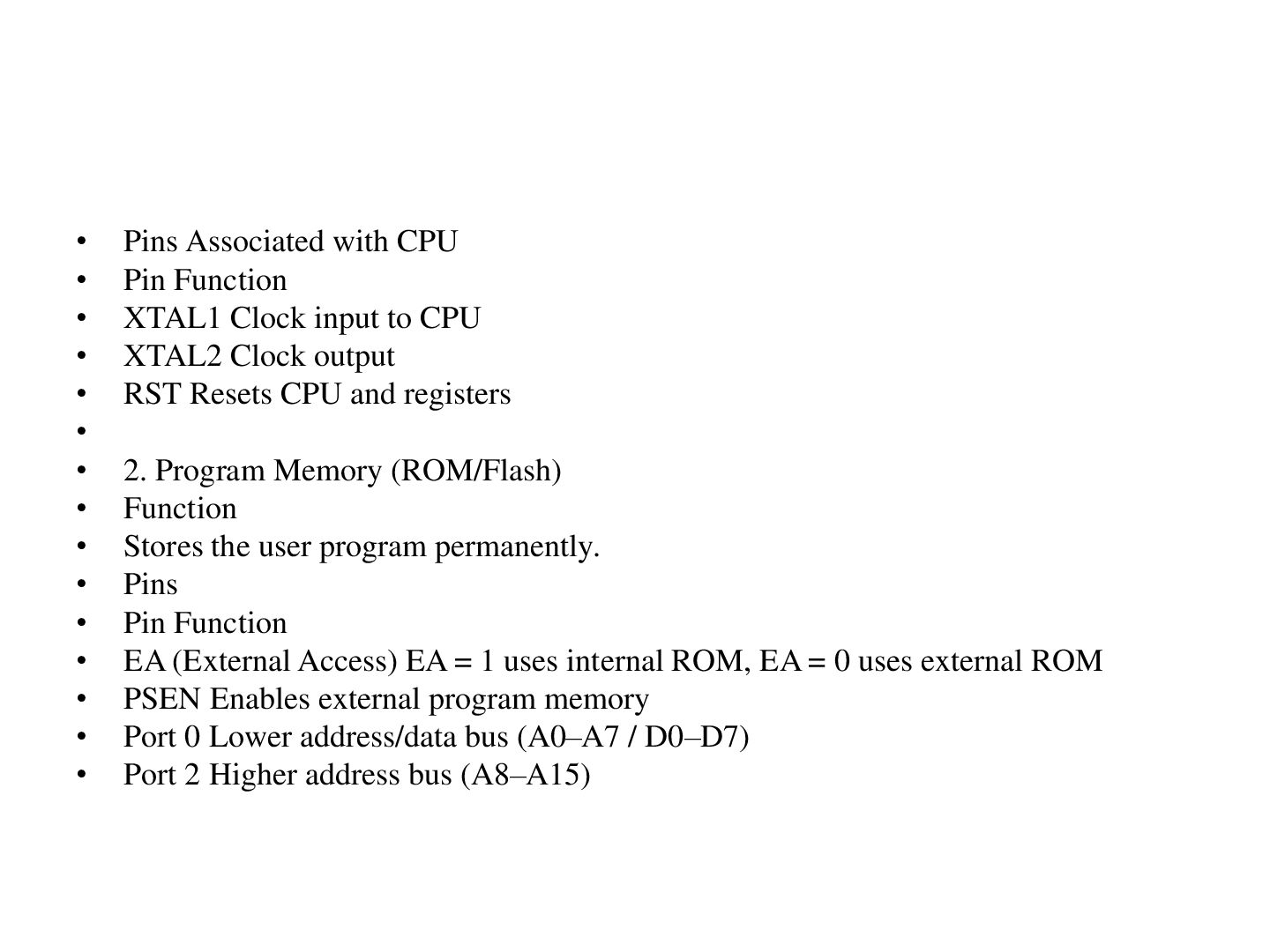
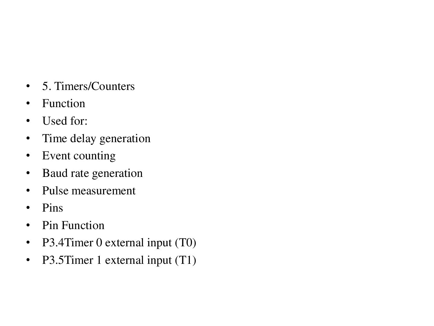
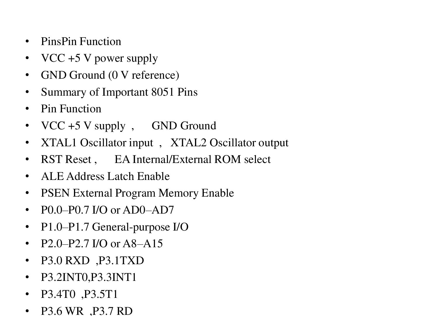
• • • • • Pins Associated with CPU Pin Function XTAL1 Clock input to CPU XTAL2 Clock output RST Resets CPU and registers 2. Program Memory (ROM/Flash) Function Stores the user program permanently. Pins Pin Function EA (External Access) EA = 1 uses internal ROM, EA = 0 uses external ROM PSEN Enables external program memory Port 0 Lower address/data bus (A0–A7 / D0–D7) Port 2 Higher address bus (A8–A15)
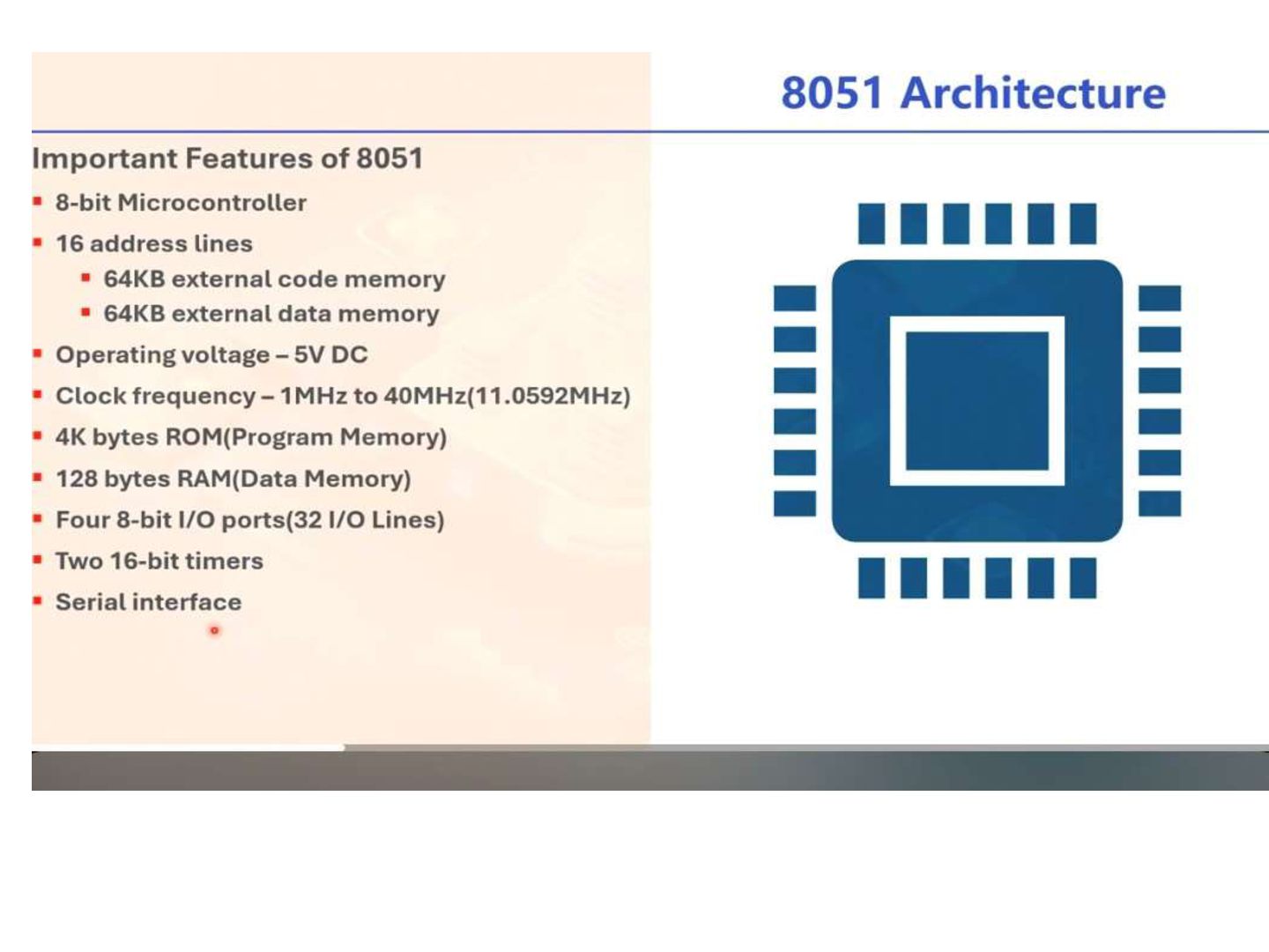
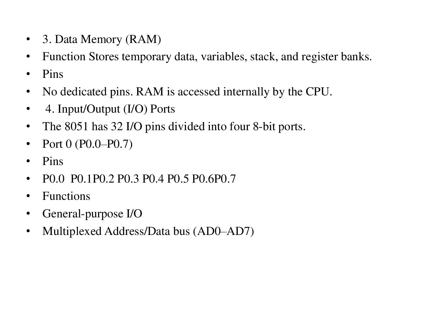
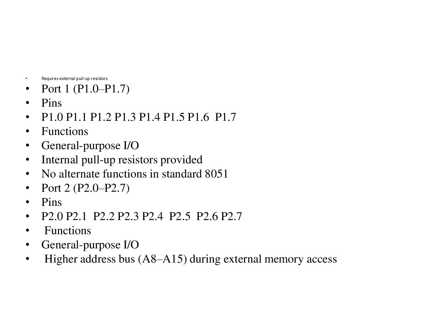
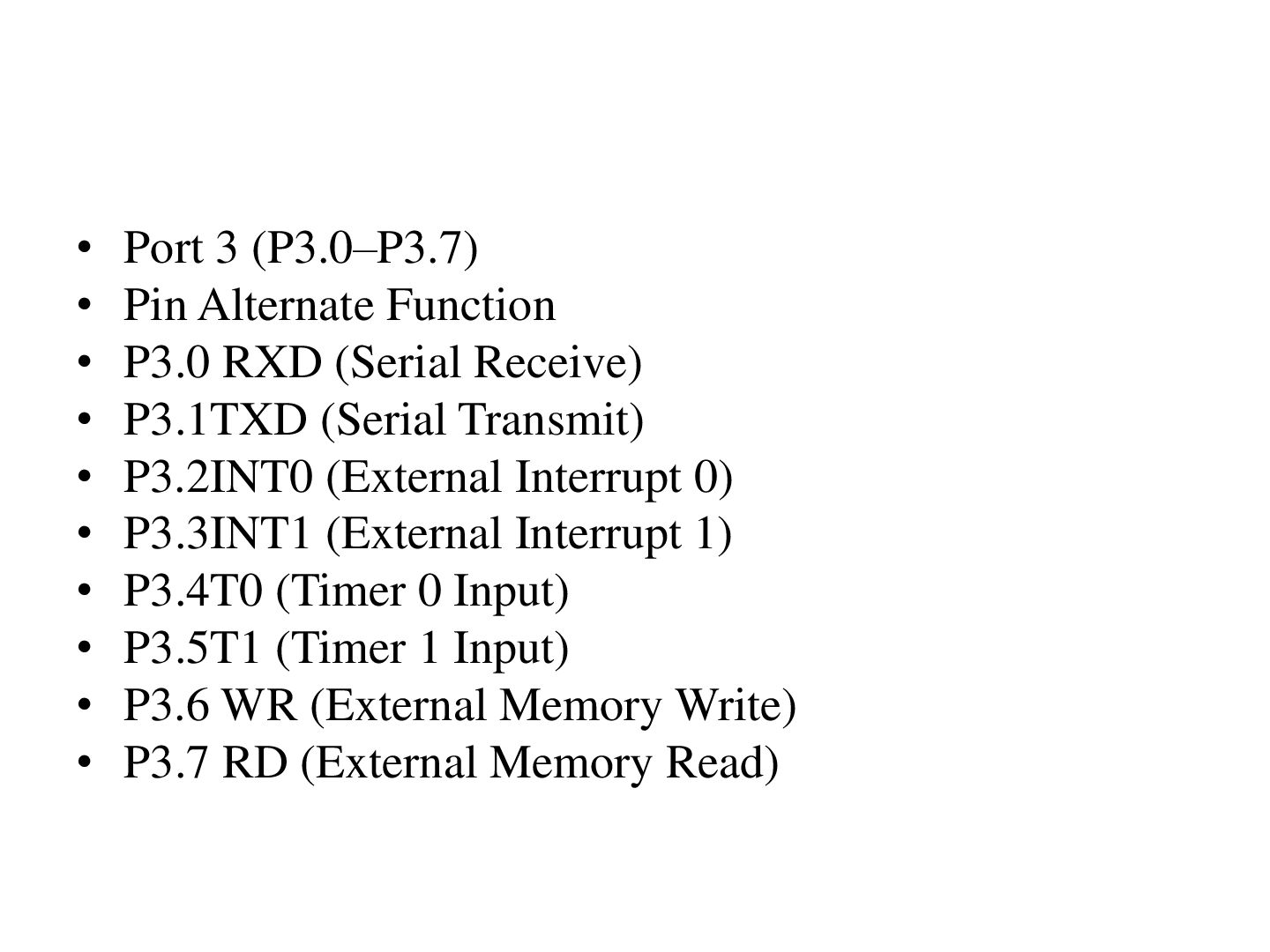
• • 3. Data Memory (RAM) Function Stores temporary data, variables, stack, and register banks. Pins No dedicated pins. RAM is accessed internally by the CPU. 4. Input/Output (I/O) Ports The 8051 has 32 I/O pins divided into four 8-bit ports. Port 0 (P0.0–P0.7) Pins P0.0 P0.1P0.2 P0.3 P0.4 P0.5 P0.6P0.7 Functions General-purpose I/O Multiplexed Address/Data bus (AD0–AD7)
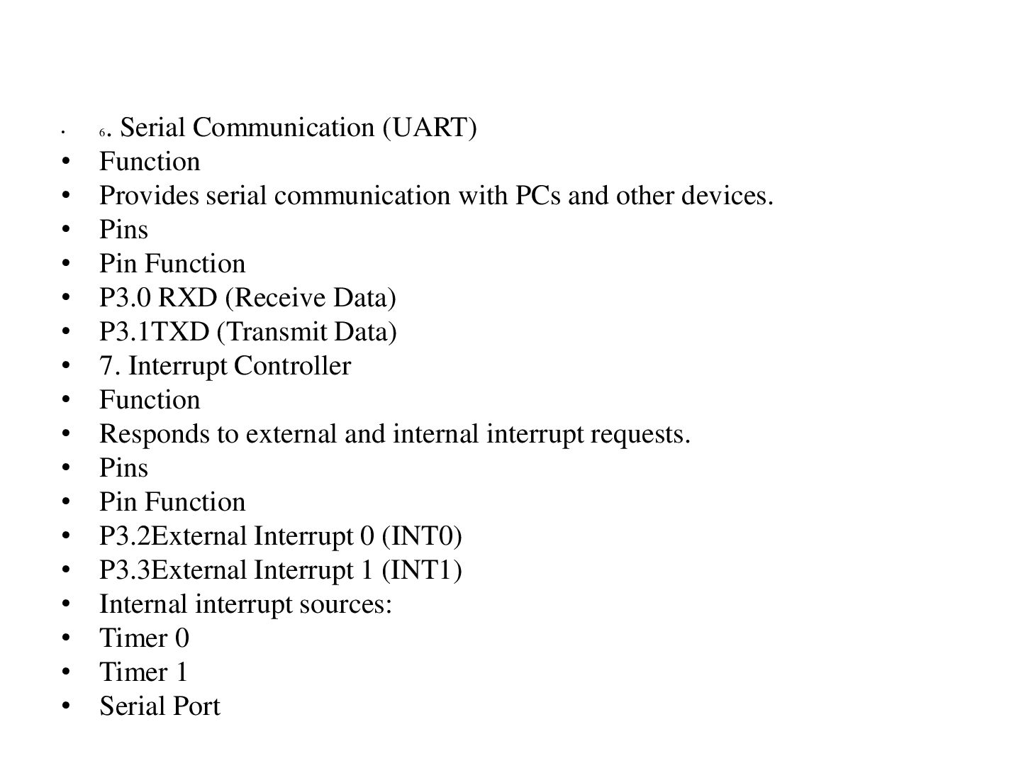
• • • • • • • • . Serial Communication (UART) Function Provides serial communication with PCs and other devices. Pins Pin Function P3.0 RXD (Receive Data) P3.1TXD (Transmit Data) 7. Interrupt Controller Function Responds to external and internal interrupt requests. Pins Pin Function P3.2External Interrupt 0 (INT0) P3.3External Interrupt 1 (INT1) Internal interrupt sources: Timer 0 Timer 1 Serial Port 6
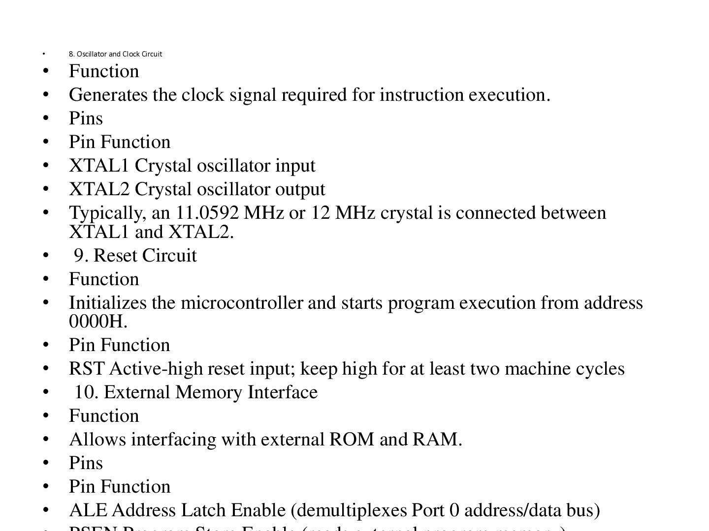
• • • • • • • • • 8. Oscillator and Clock Circuit Function Generates the clock signal required for instruction execution. Pins Pin Function XTAL1 Crystal oscillator input XTAL2 Crystal oscillator output Typically, an 11.0592 MHz or 12 MHz crystal is connected between XTAL1 and XTAL2. 9. Reset Circuit Function Initializes the microcontroller and starts program execution from address 0000H. Pin Function RST Active-high reset input; keep high for at least two machine cycles 10. External Memory Interface Function Allows interfacing with external ROM and RAM. Pins Pin Function ALE Address Latch Enable (demultiplexes Port 0 address/data bus)
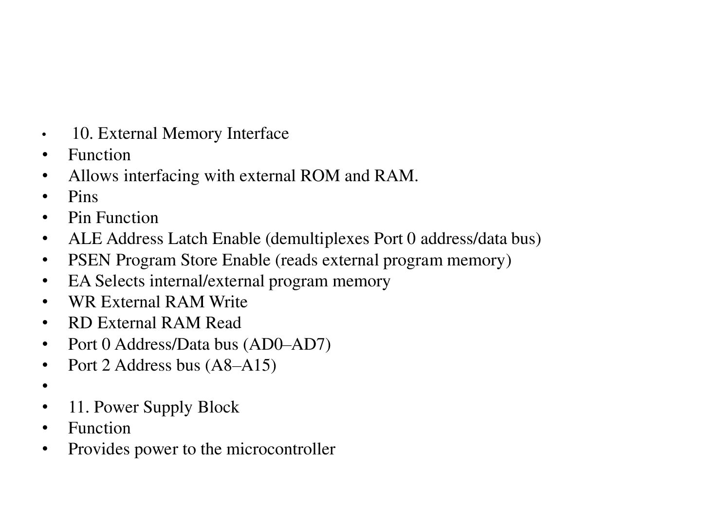
• • • • • • 10. External Memory Interface Function Allows interfacing with external ROM and RAM. Pins Pin Function ALE Address Latch Enable (demultiplexes Port 0 address/data bus) PSEN Program Store Enable (reads external program memory) EA Selects internal/external program memory WR External RAM Write RD External RAM Read Port 0 Address/Data bus (AD0–AD7) Port 2 Address bus (A8–A15) 11. Power Supply Block Function Provides power to the microcontroller


 anjalimagdum
 lauravandoore
 holman
 trallard
 szymonslowik
 eileencodes
 bcantrill
 dougneiner
 codingconduct
 paigeccino
 seathinner
 mza
 tapps