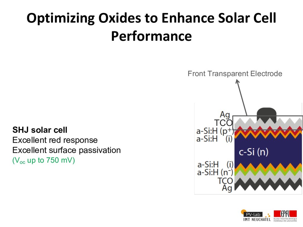
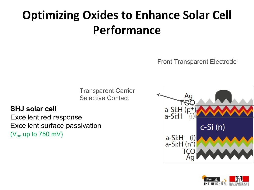
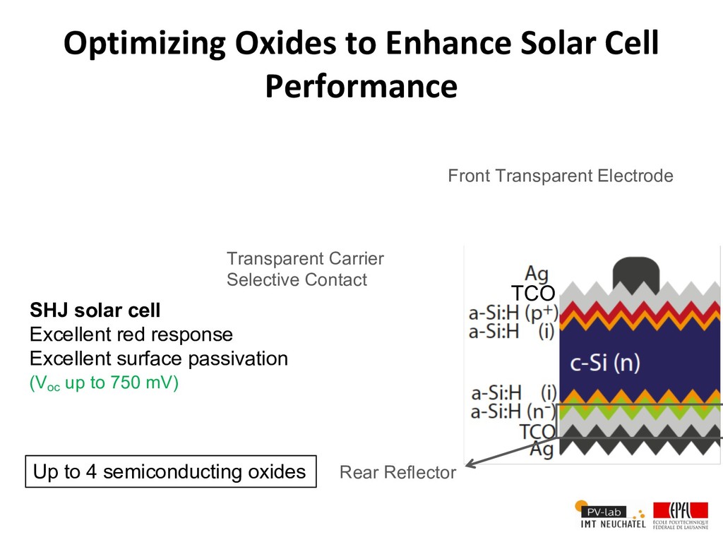
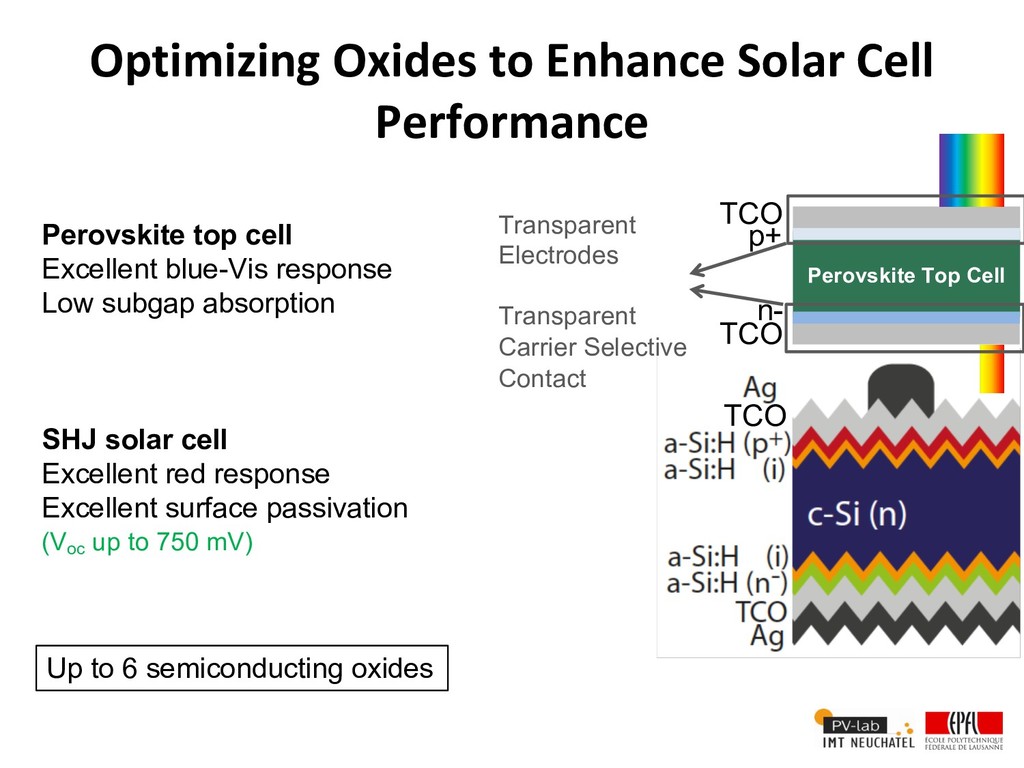
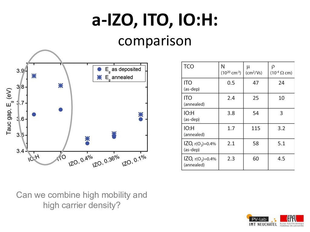
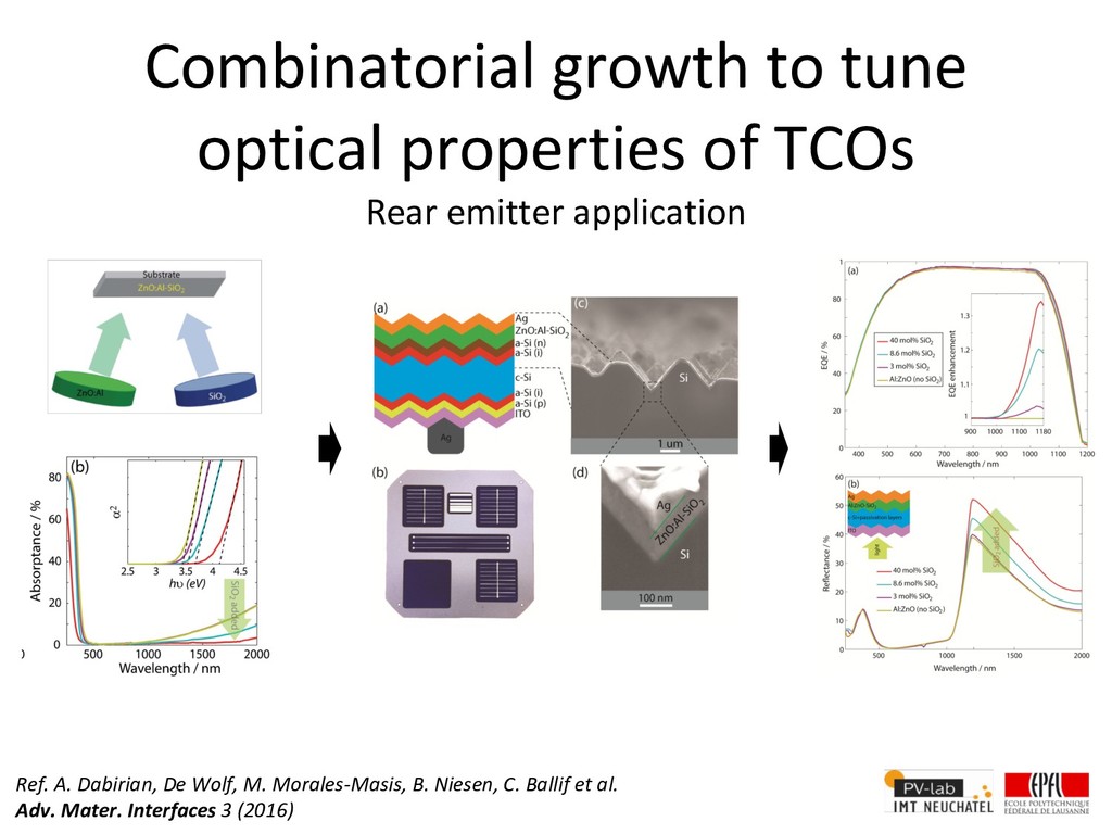
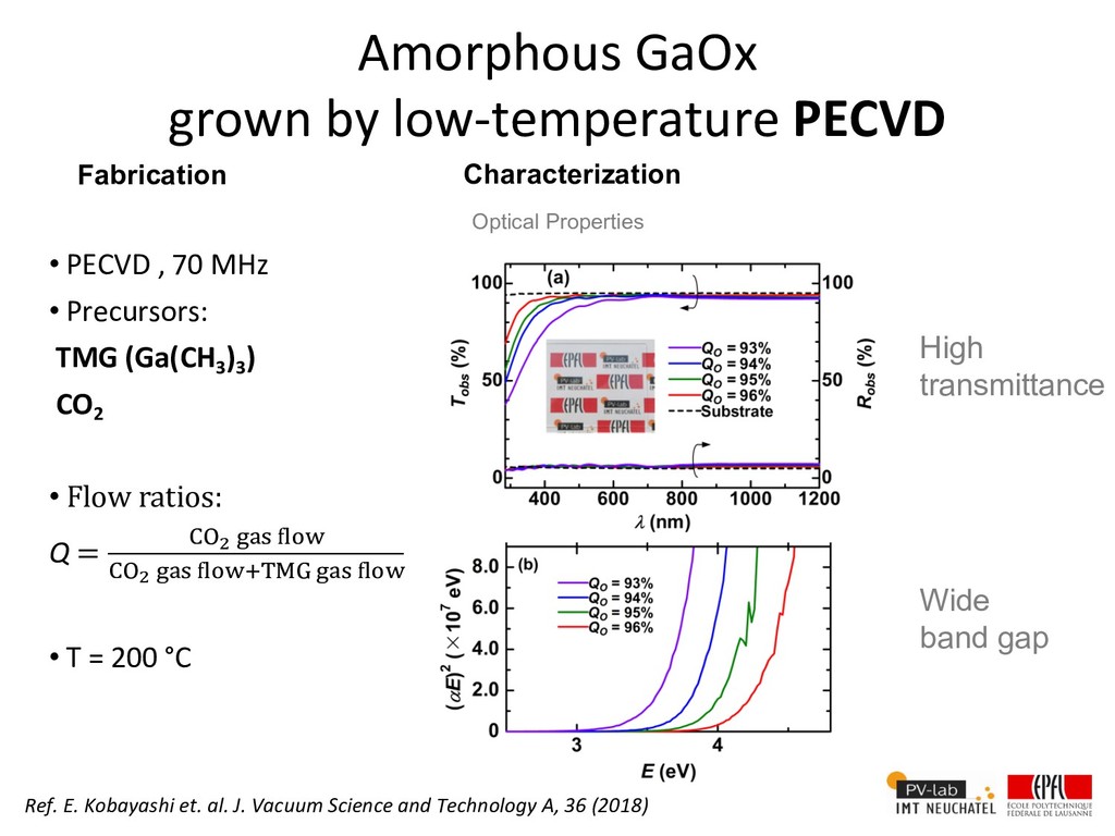
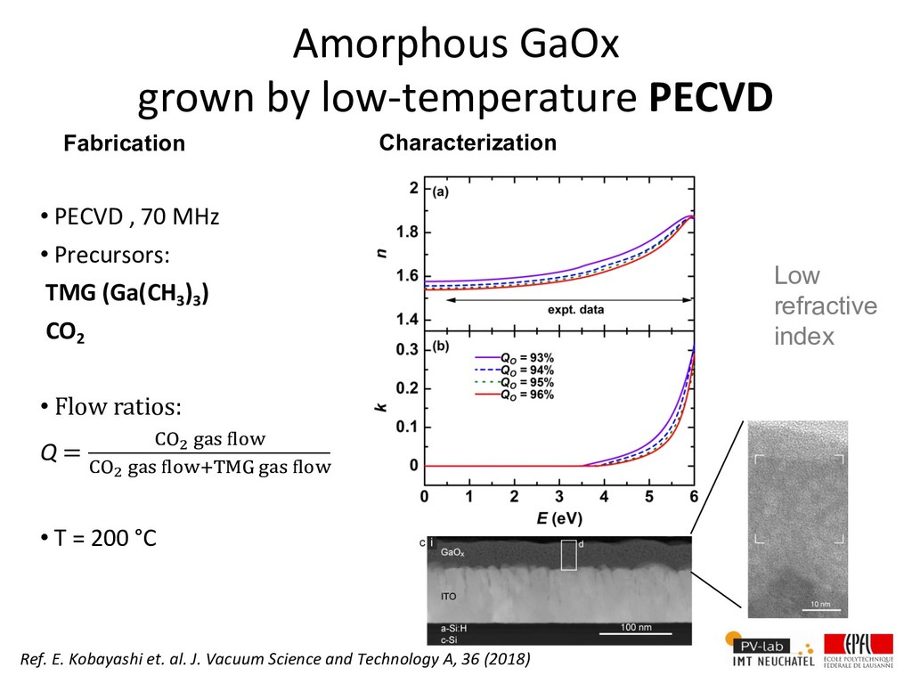
(Voc up to 750 mV) Front Transparent Electrode Transparent Carrier Selective Contact Rear Reflector Up to 4 semiconducting oxides Optimizing Oxides to Enhance Solar Cell Performance
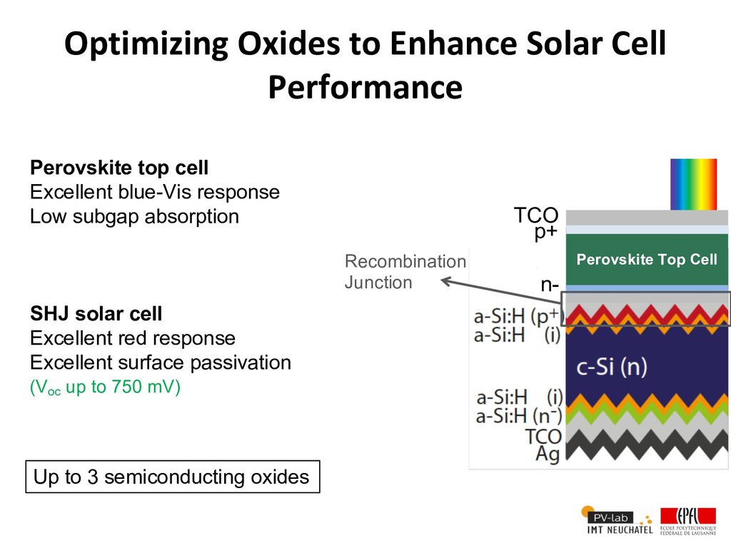
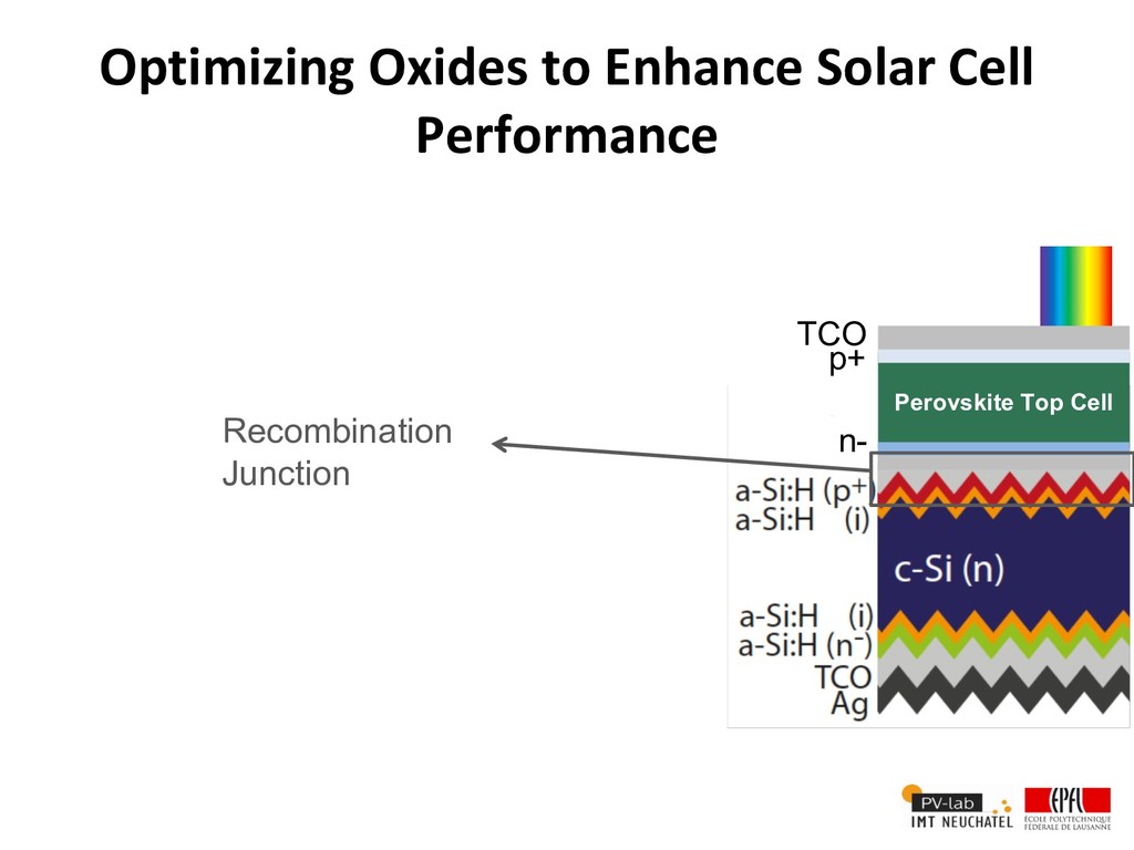
Excellent red response Excellent surface passivation (Voc up to 750 mV) Perovskite top cell Excellent blue-Vis response Low subgap absorption TCO Recombination Junction Perovskite Top Cell TCO p+ n- Up to 3 semiconducting oxides
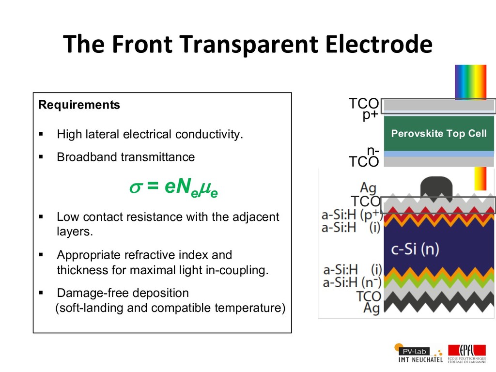
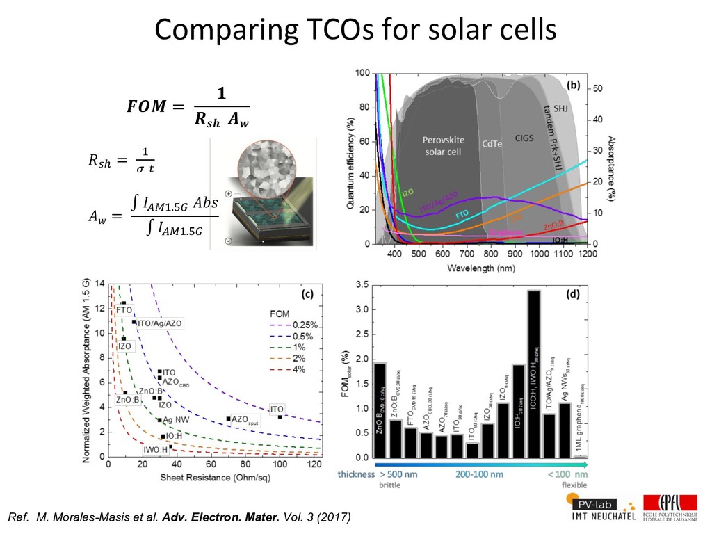
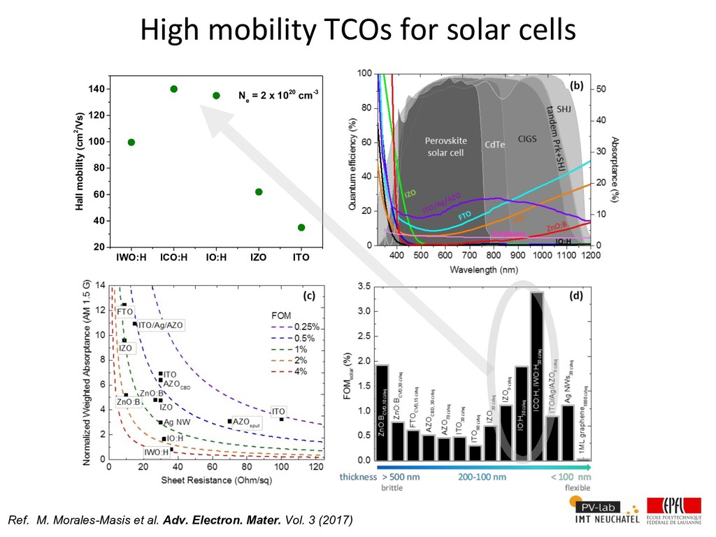
p+ n- Requirements § High lateral electrical conductivity. § Broadband transmittance § Low contact resistance with the adjacent layers. § Appropriate refractive index and thickness for maximal light in-coupling. § Damage-free deposition (soft-landing and compatible temperature) s = eN e µ e
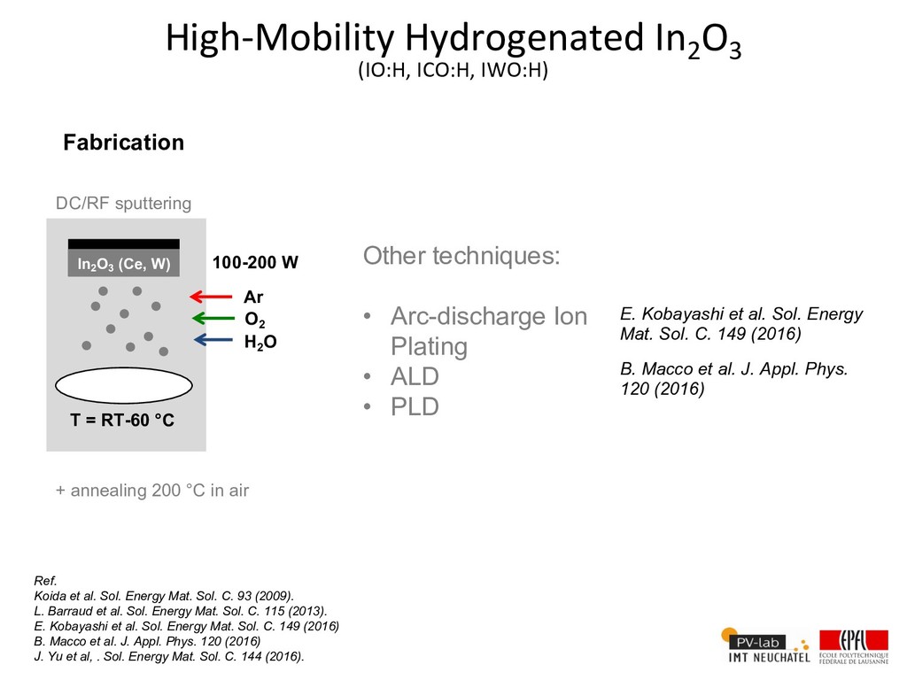
O3 (Ce, W) Ar T = RT-60 °C 100-200 W O2 H2 O DC/RF sputtering Fabrication Ref. Koida et al. Sol. Energy Mat. Sol. C. 93 (2009). L. Barraud et al. Sol. Energy Mat. Sol. C. 115 (2013). E. Kobayashi et al. Sol. Energy Mat. Sol. C. 149 (2016) B. Macco et al. J. Appl. Phys. 120 (2016) J. Yu et al, . Sol. Energy Mat. Sol. C. 144 (2016). Other techniques: • Arc-discharge Ion Plating • ALD • PLD + annealing 200 °C in air E. Kobayashi et al. Sol. Energy Mat. Sol. C. 149 (2016) B. Macco et al. J. Appl. Phys. 120 (2016)
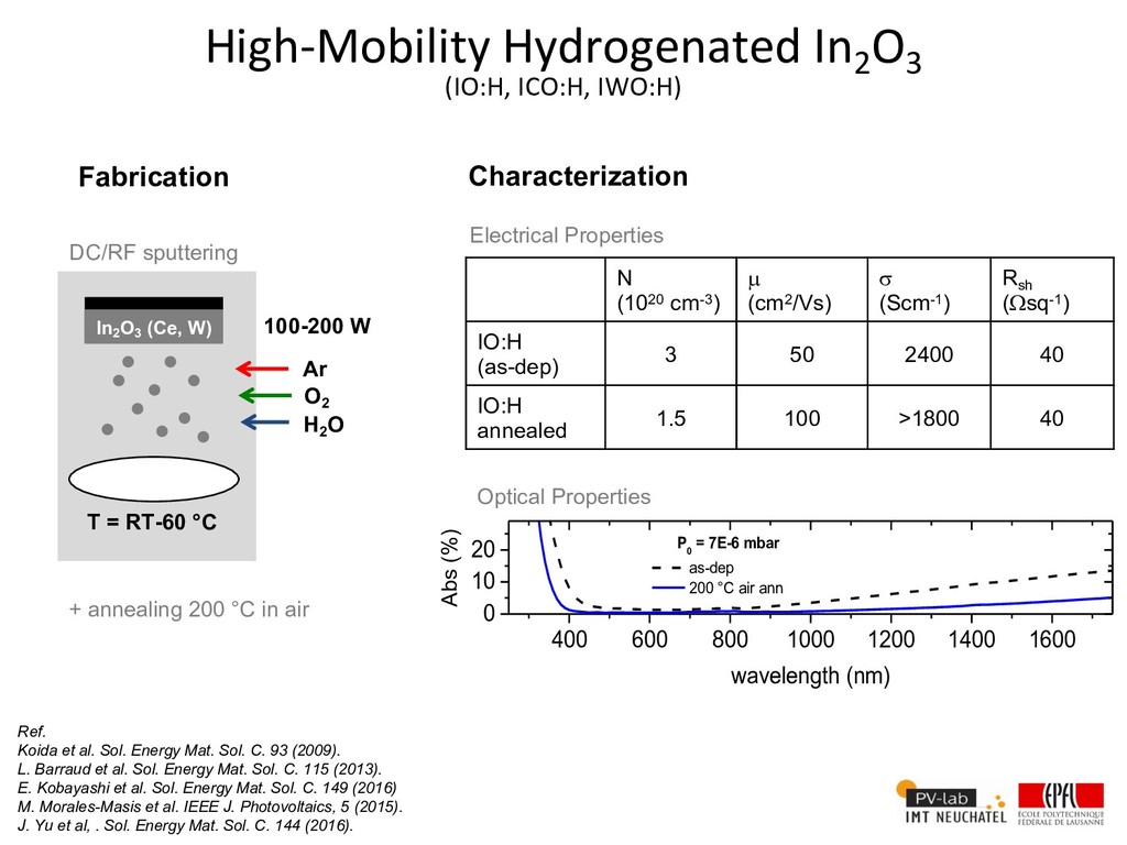
O3 (Ce, W) Ar T = RT-60 °C 100-200 W O2 H2 O DC/RF sputtering Fabrication 0 10 20 0 10 20 0 10 20 400 600 800 1000 1200 1400 1600 0 10 20 P 0 = 1E-7 mbar as-dep 200 °C air ann Absorptance (%) P 0 = 1.45E-6 mbar as-dep 200 °C air ann P 0 = 2.4E-6 mbar as-dep 200 °C air ann wavelength (nm) P 0 = 7E-6 mbar as-dep 200 °C air ann Characterization N (1020 cm-3) µ (cm2/Vs) s (Scm-1) Rsh (Wsq-1) IO:H (as-dep) 3 50 2400 40 IO:H annealed 1.5 100 >1800 40 Electrical Properties Optical Properties Abs (%) + annealing 200 °C in air Ref. Koida et al. Sol. Energy Mat. Sol. C. 93 (2009). L. Barraud et al. Sol. Energy Mat. Sol. C. 115 (2013). E. Kobayashi et al. Sol. Energy Mat. Sol. C. 149 (2016) M. Morales-Masis et al. IEEE J. Photovoltaics, 5 (2015). J. Yu et al, . Sol. Energy Mat. Sol. C. 144 (2016).
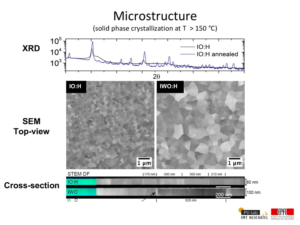
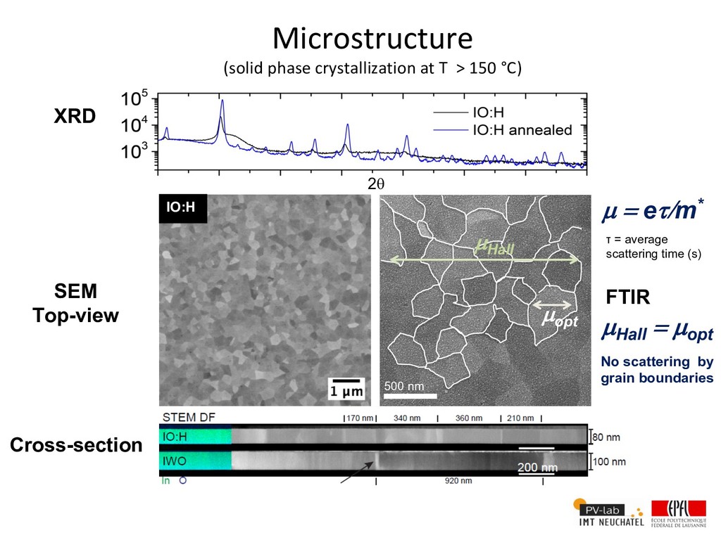
Top-view Cross-section IWO:H IO:H XRD 2q 500 nm µ Hall µ opt µ Hall = µ opt No scattering by grain boundaries µ = et/m* τ = average scattering time (s) FTIR
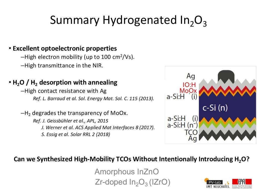
–High electron mobility (up to 100 cm2/Vs). –High transmittance in the NIR. • H 2 O / H 2 desorption with annealing –High contact resistance with Ag Ref. L. Barraud et al. Sol. Energy Mat. Sol. C. 115 (2013). –H2 degrades the transparency of MoOx. Ref. J. Geissbühler et al., APL, 2015 J. Werner et al. ACS Applied Mat Interfaces 8 (2017). S. Essig et al. Solar RRL 2 (2018) IO:H MoOx Can we Synthesized High-Mobility TCOs Without Intentionally Introducing H 2 O? Amorphous InZnO Zr-doped In2 O3 (IZrO)
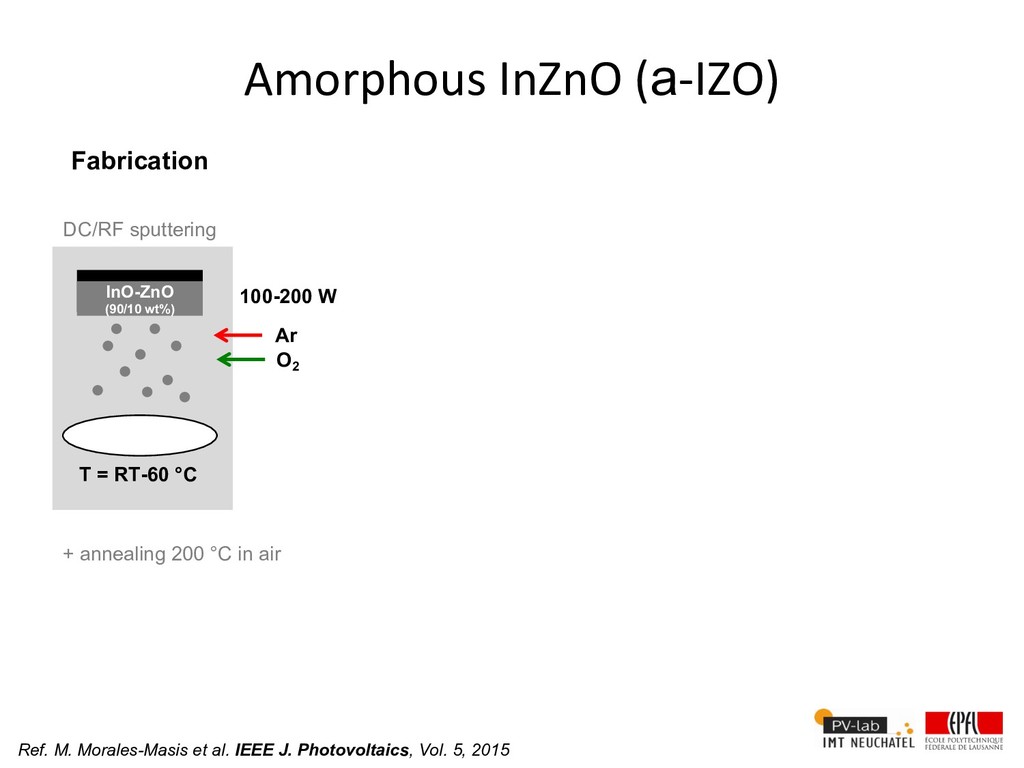
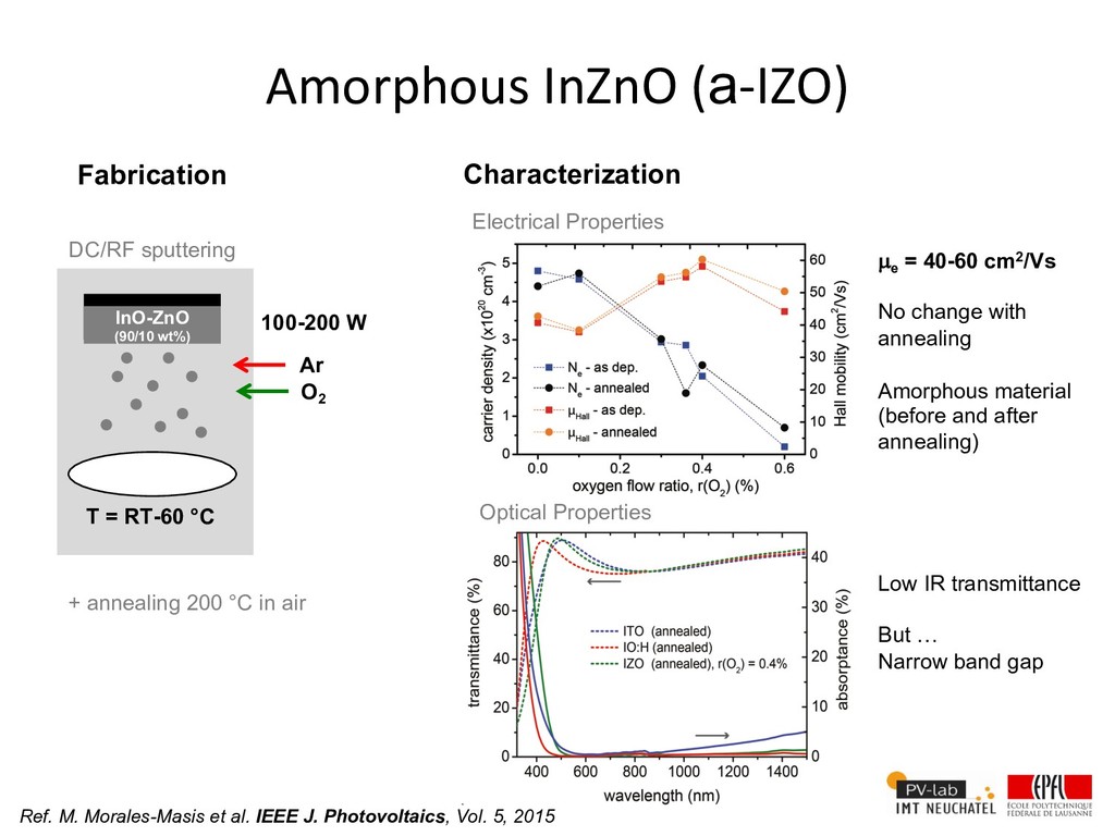
O2 DC/RF sputtering Fabrication + annealing 200 °C in air Amorphous InZnO (a-IZO) Characterization Electrical Properties Optical Properties µ e = 40-60 cm2/Vs No change with annealing Amorphous material (before and after annealing) Low IR transmittance But … Narrow band gap Ref. M. Morales-Masis et al. IEEE J. Photovoltaics, Vol. 5, 2015
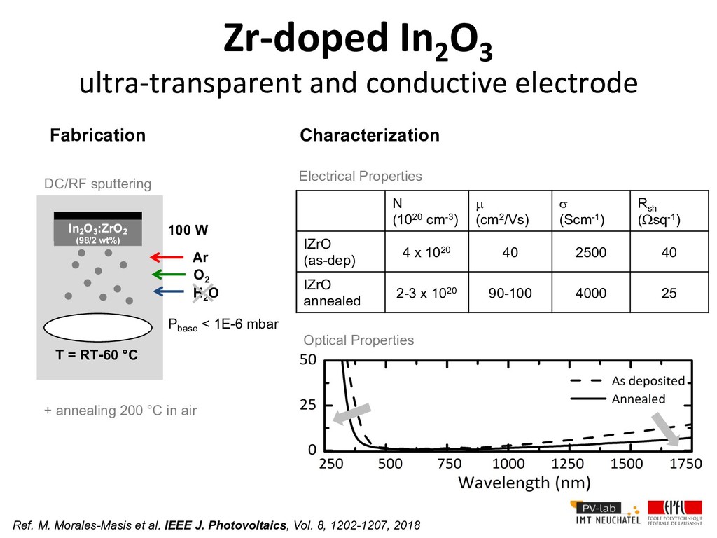
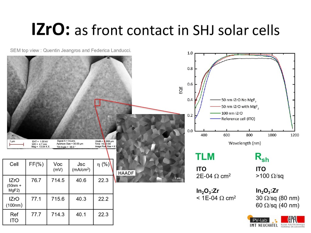
O3 :ZrO2 (98/2 wt%) Ar T = RT-60 °C 100 W O 2 H 2 O DC/RF sputtering Fabrication + annealing 200 °C in air Pbase < 1E-6 mbar N (1020 cm-3) µ (cm2/Vs) s (Scm-1) Rsh (Wsq-1) IZrO (as-dep) 4 x 10²⁰ 40 2500 40 IZrO annealed 2-3 x 10²⁰ 90-100 4000 25 Characterization Electrical Properties Optical Properties Ref. M. Morales-Masis et al. IEEE J. Photovoltaics, Vol. 8, 1202-1207, 2018
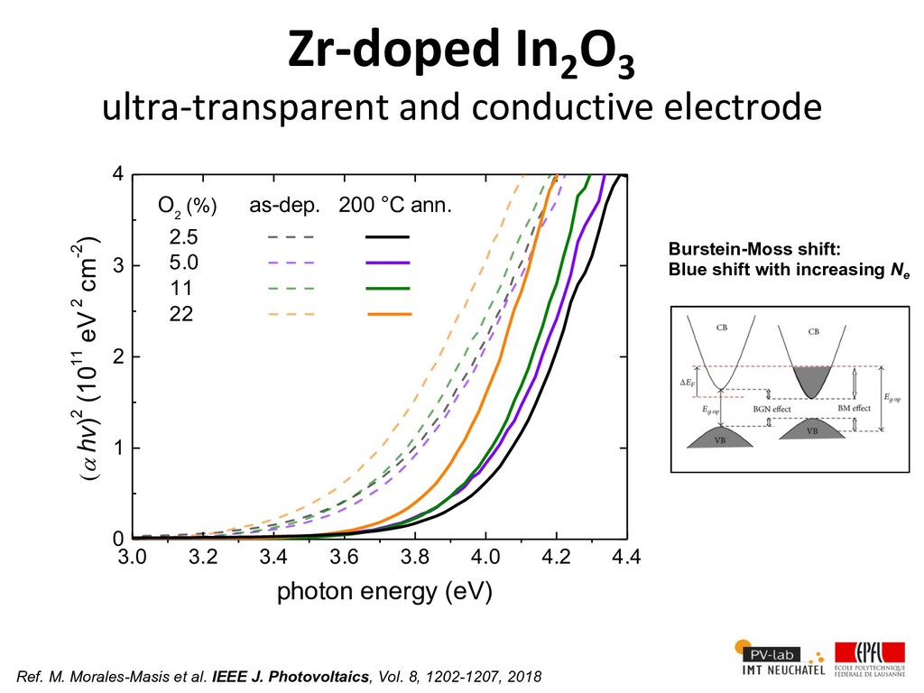
2 3 4 O 2 (%) as-dep. 200 °C ann. 2.5 5.0 11 22 (a hv)2 (1011 eV 2 cm-2) photon energy (eV) Burstein-Moss shift: Blue shift with increasing N e Zr-doped In 2 O 3 ultra-transparent and conductive electrode Ref. M. Morales-Masis et al. IEEE J. Photovoltaics, Vol. 8, 1202-1207, 2018
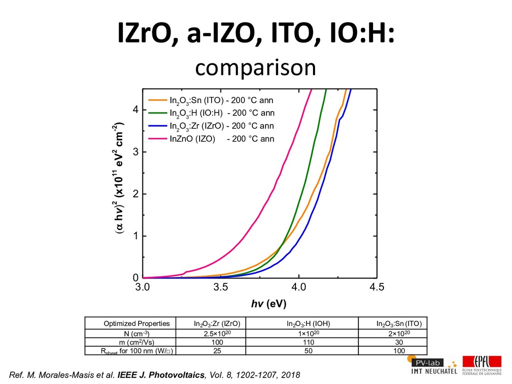
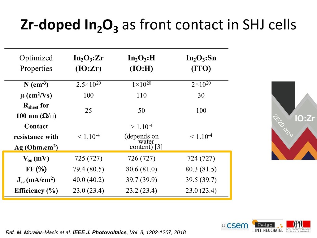
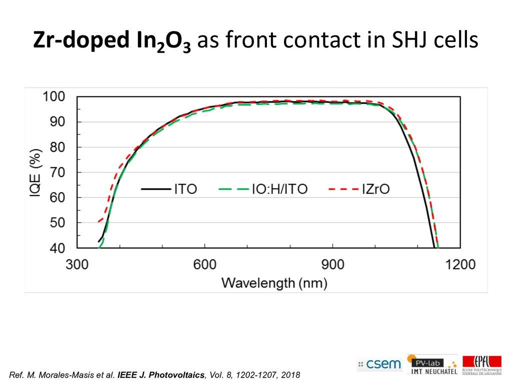
1 2 3 4 (a hv)2 (x1011 eV2 cm-2) hv (eV) In 2 O 3 :Sn (ITO) - 200 °C ann In 2 O 3 :H (IO:H) - 200 °C ann In 2 O 3 :Zr (IZrO) - 200 °C ann InZnO (IZO) - 200 °C ann Optimized Properties In2 O3 :Zr (IZrO) In2 O3 :H (IOH) In2 O3 :Sn (ITO) N (cm-3) 2.5×10²⁰ 1×10²⁰ 2×10²⁰ m (cm2/Vs) 100 110 30 Rsheet for 100 nm (W/□) 25 50 100 Ref. M. Morales-Masis et al. IEEE J. Photovoltaics, Vol. 8, 1202-1207, 2018
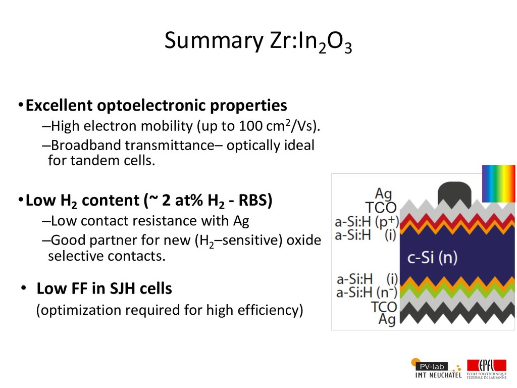
to 100 cm2/Vs). –Broadband transmittance– optically ideal for tandem cells. •Low H2 content (~ 2 at% H2 - RBS) –Low contact resistance with Ag –Good partner for new (H2 –sensitive) oxide selective contacts. • Low FF in SJH cells (optimization required for high efficiency) TCO
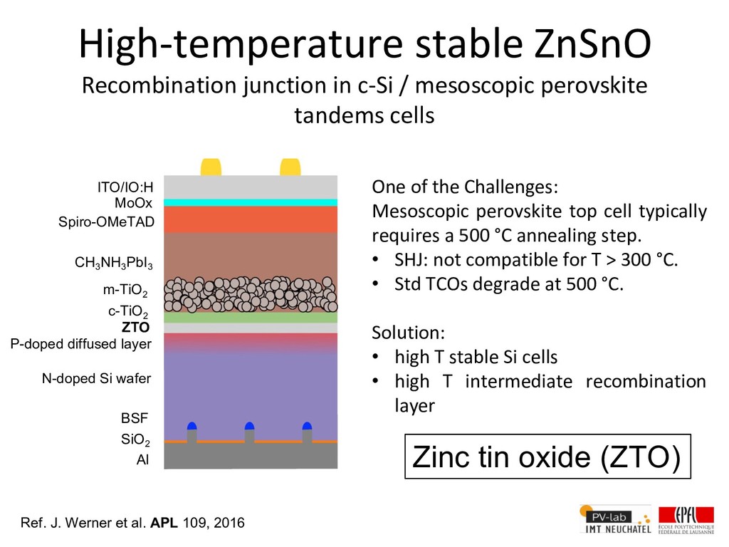
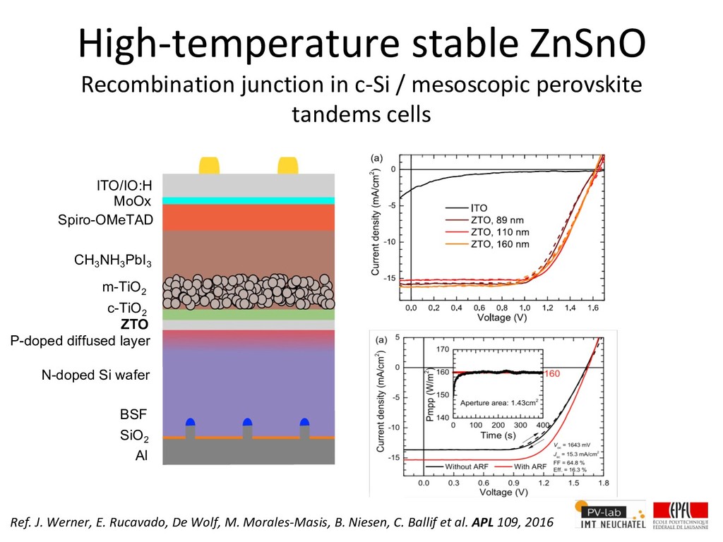
tandems cells One of the Challenges: Mesoscopic perovskite top cell typically requires a 500 °C annealing step. • SHJ: not compatible for T > 300 °C. • Std TCOs degrade at 500 °C. Solution: • high T stable Si cells • high T intermediate recombination layer ITO/IO:H MoOx Spiro-OMeTAD CH3 NH3 PbI3 m-TiO2 c-TiO2 ZTO P-doped diffused layer N-doped Si wafer BSF SiO2 Al Zinc tin oxide (ZTO) Ref. J. Werner et al. APL 109, 2016
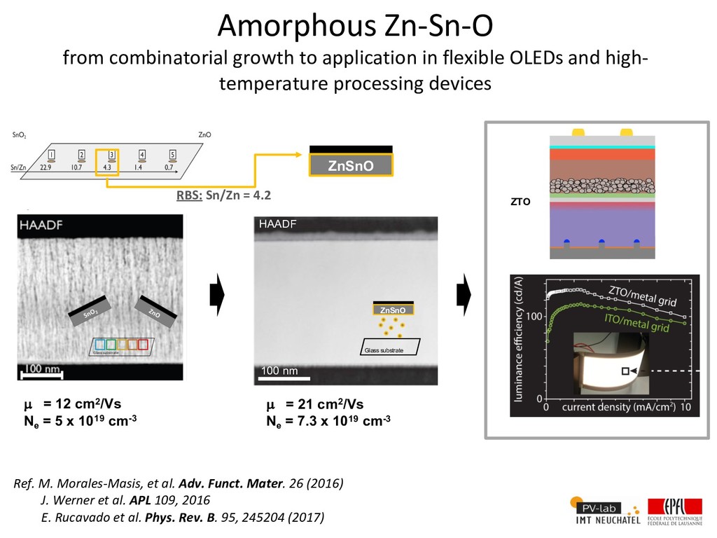
5 x 1019 cm-3 µ = 21 cm2/Vs Ne = 7.3 x 1019 cm-3 100 nm HAADF ZnSnO Glass substrate Amorphous Zn-Sn-O from combinatorial growth to application in flexible OLEDs and high- temperature processing devices Ref. M. Morales-Masis, et al. Adv. Funct. Mater. 26 (2016) J. Werner et al. APL 109, 2016 E. Rucavado et al. Phys. Rev. B. 95, 245204 (2017) ZTO ZnSnO RBS: Sn/Zn = 4.2
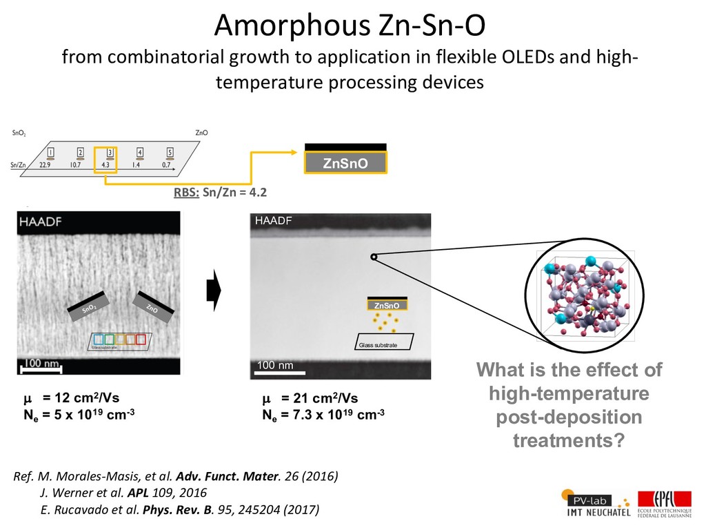
5 x 1019 cm-3 µ = 21 cm2/Vs Ne = 7.3 x 1019 cm-3 100 nm HAADF ZnSnO Glass substrate Amorphous Zn-Sn-O from combinatorial growth to application in flexible OLEDs and high- temperature processing devices Ref. M. Morales-Masis, et al. Adv. Funct. Mater. 26 (2016) J. Werner et al. APL 109, 2016 E. Rucavado et al. Phys. Rev. B. 95, 245204 (2017) ZnSnO RBS: Sn/Zn = 4.2 What is the effect of high-temperature post-deposition treatments?
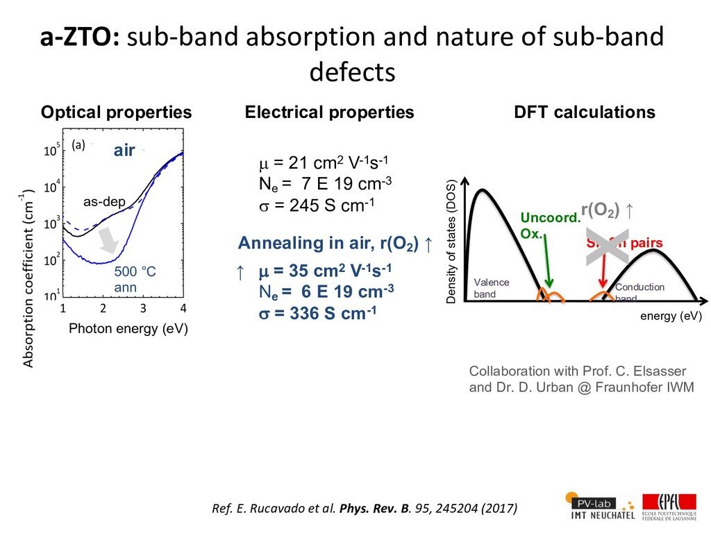
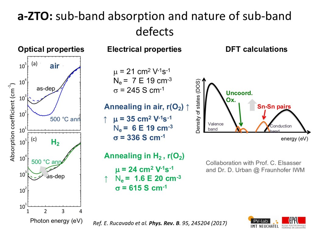
Electrical properties air N2 H2 as-dep 500 °C ann 500 °C ann as-dep µ = 21 cm2 V-1s-1 Ne = 7 E 19 cm-3 s = 245 S cm-1 Annealing in air, r(O2 ) ↑ ↑ µ = 35 cm2 V-1s-1 N e = 6 E 19 cm-3 s = 336 S cm-1 Annealing in H2 , r(O2 ) ↑ ↑ µ = 24 cm2 V-1s-1 N e = 1.6 E 20 cm-3 s = 615 S cm-1 500 °C ann as-dep DFT calculations Density of states (DOS) energy (eV) Conducti on band Valence band Conduction band Sn-Sn pairs Uncoord. Ox. Photon energy (eV) X r(O2 ) ↑ Collaboration with Prof. C. Elsasser and Dr. D. Urban @ Fraunhofer IWM Ref. E. Rucavado et al. Phys. Rev. B. 95, 245204 (2017)
Electrical properties air N2 H2 as-dep 500 °C ann 500 °C ann as-dep µ = 21 cm2 V-1s-1 Ne = 7 E 19 cm-3 s = 245 S cm-1 Annealing in air, r(O2 ) ↑ ↑ µ = 35 cm2 V-1s-1 N e = 6 E 19 cm-3 s = 336 S cm-1 Annealing in H2 , r(O2 ) ↑ µ = 24 cm2 V-1s-1 N e = 1.6 E 20 cm-3 s = 615 S cm-1 500 °C ann as-dep DFT calculations Density of states (DOS) energy (eV) Conducti on band Valence band Conduction band Sn-Sn pairs Uncoord. Ox. Photon energy (eV) Ref. E. Rucavado et al. Phys. Rev. B. 95, 245204 (2017) Collaboration with Prof. C. Elsasser and Dr. D. Urban @ Fraunhofer IWM
tandems cells ITO/IO:H MoOx Spiro-OMeTAD CH 3 NH 3 PbI 3 m-TiO 2 c-TiO 2 ZTO P-doped diffused layer N-doped Si wafer BSF SiO2 Al Ref. J. Werner, E. Rucavado, De Wolf, M. Morales-Masis, B. Niesen, C. Ballif et al. APL 109, 2016
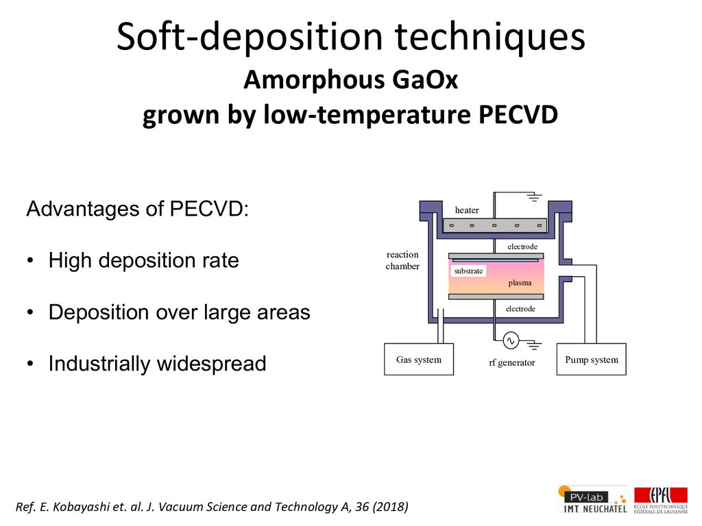
PECVD: • High deposition rate • Deposition over large areas • Industrially widespread Gas system rf generator electrode electrode substrate heater Pump system reaction chamber plasma Ref. E. Kobayashi et. al. J. Vacuum Science and Technology A, 36 (2018)
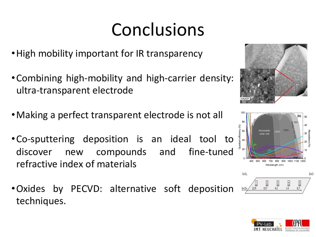
high-carrier density: ultra-transparent electrode •Making a perfect transparent electrode is not all •Co-sputtering deposition is an ideal tool to discover new compounds and fine-tuned refractive index of materials •Oxides by PECVD: alternative soft deposition techniques.


 mmoralesmasis
 dugsong
 reverentgeek
 eileencodes
 palkan
 skipperchong
 smashingmag
 keavy
 csswizardry
 helenjbeal
 holman
 axbom
 maltzj