is faulty you’ll know it faster than if you sent it out to be made and a week later you’re out cash and time) COASTERS • learn more about electricity (close component placement/ perf boards) • once your circuit is down, it’s locked down (less sleepless nights for you finding the *one wire that was in the wrong place • learn your circuit • circuits are attractive and neat • next level (form and function/sparks ideas) • your friends will be impressed Monday, April 1, 2013
Here it’s nice to print out your layout on regular paper, and “fake” populate the board command lines: route (width should be .04 - .016 for good traces) *make sure to use ripup (click trace you want to rip up) ripup * (rips up all traces) auto (auto routes -recommended only if you’re stuck) mov cntrl + click while in mov mode = rotation polygon name > click on polygon> *type GND>ENTER i (information)> isolate (drop down)> .016 rats nest get close Monday, April 1, 2013
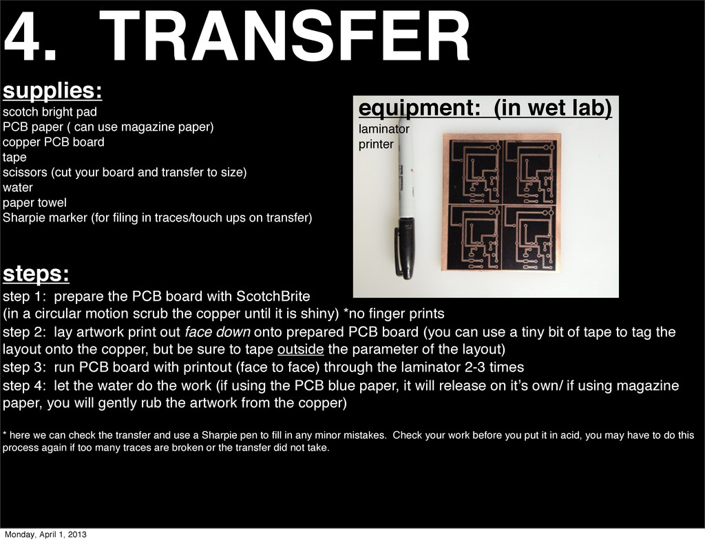
bright pad PCB paper ( can use magazine paper) copper PCB board tape scissors (cut your board and transfer to size) water paper towel Sharpie marker (for filing in traces/touch ups on transfer) steps: step 1: prepare the PCB board with ScotchBrite (in a circular motion scrub the copper until it is shiny) *no finger prints step 2: lay artwork print out face down onto prepared PCB board (you can use a tiny bit of tape to tag the layout onto the copper, but be sure to tape outside the parameter of the layout) step 3: run PCB board with printout (face to face) through the laminator 2-3 times = step 4: let the water do the work (if using the PCB blue paper, it will release on itʼs own/ if using magazine paper, you will gently rub the artwork from the copper) * here we can check the transfer and use a Sharpie pen to fill in any minor mistakes. Check your work before you put it in acid, you may have to do this process again if too many traces are broken or the transfer did not take. Monday, April 1, 2013
of old acid) * bin in the shop empty container to size (for agitation and used acid) acid (mixed or at RadioShack) GLOVES!!!! If your transfer is OK, you can proceed to step 1 of the etching process. PREP: (microwave acid for 20-30 seconds before putting board in acid) step 1: acid bath agitation-- USE GLOVES!! step 2: use gloves. step 3: rinse (no touching) step 4: pat dry (the transfer is not quite set yet, if you are not gentle, the ink could rub off) step 5: scotch bright off black printed board to reveal copper. Monday, April 1, 2013