• save money (if your board is faulty you’ll know it faster than if you sent it out to be made and a week later you’re out cash and time) • learn more about electricity (component placement) • learn your circuit • once your circuit is down, it’s locked down (less sleepless nights for you finding the *one wire that was in the wrong place • circuits are attractive and neat • next level (form and function) • your friends will be impressed Sunday, March 31, 2013
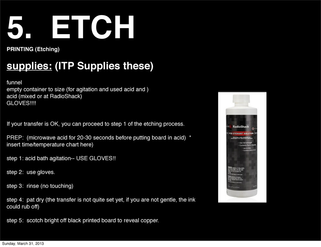
container to size (for agitation and used acid and ) acid (mixed or at RadioShack) GLOVES!!!! If your transfer is OK, you can proceed to step 1 of the etching process. PREP: (microwave acid for 20-30 seconds before putting board in acid) * insert time/temperature chart here) step 1: acid bath agitation-- USE GLOVES!! step 2: use gloves. step 3: rinse (no touching) step 4: pat dry (the transfer is not quite set yet, if you are not gentle, the ink could rub off) step 5: scotch bright off black printed board to reveal copper. Sunday, March 31, 2013
bright pad PCB paper ( can use magazine paper) copper PCB board tape scissors (cut your board and transfer to size) water paper towel Sharpie marker (for filing in traces/touch ups on transfer) steps: step 1: prepare the PCB board with ScotchBrite (in a circular motion scrub the copper until it is shiny) step 2: lay artwork print out face down onto prepared PCB board (you can use a tiny bit of tape to tag the layout onto the copper, but be sure to tape outside the parameter of the layout) step 3: run PCB board with printout (face to face) through the laminator 2-3 times step 5: let the water do the work (if using the PCB blue paper, it will release on itʼs own/ if using magazine paper, you will gently rub the artwork from the copper) equipment: (in wet lab) laminator printer Sunday, March 31, 2013