Upgrade to Pro — share decks privately, control downloads, hide ads and more …

DataPath

Chen
October 05, 2022

 DataPath

Chen

October 05, 2022
Tweet

More Decks by Chen

Other Decks in Science

Transcript

  1. 12 First Instruction: add (e.g., add $1,$2,$3) • Add register

    file and ALU • Control (unlabeled arrows) discussed later P C Insn Mem Register File R-type s1 s2 d + 4 decoding in MIPS = wiring to the right place Op(6) Rs(5) Rt(5) Rd(5) Sh(5) Func(6)
  2. 13 Second Instruction: addi (e.g., addi $1,$2,50) • Destination register

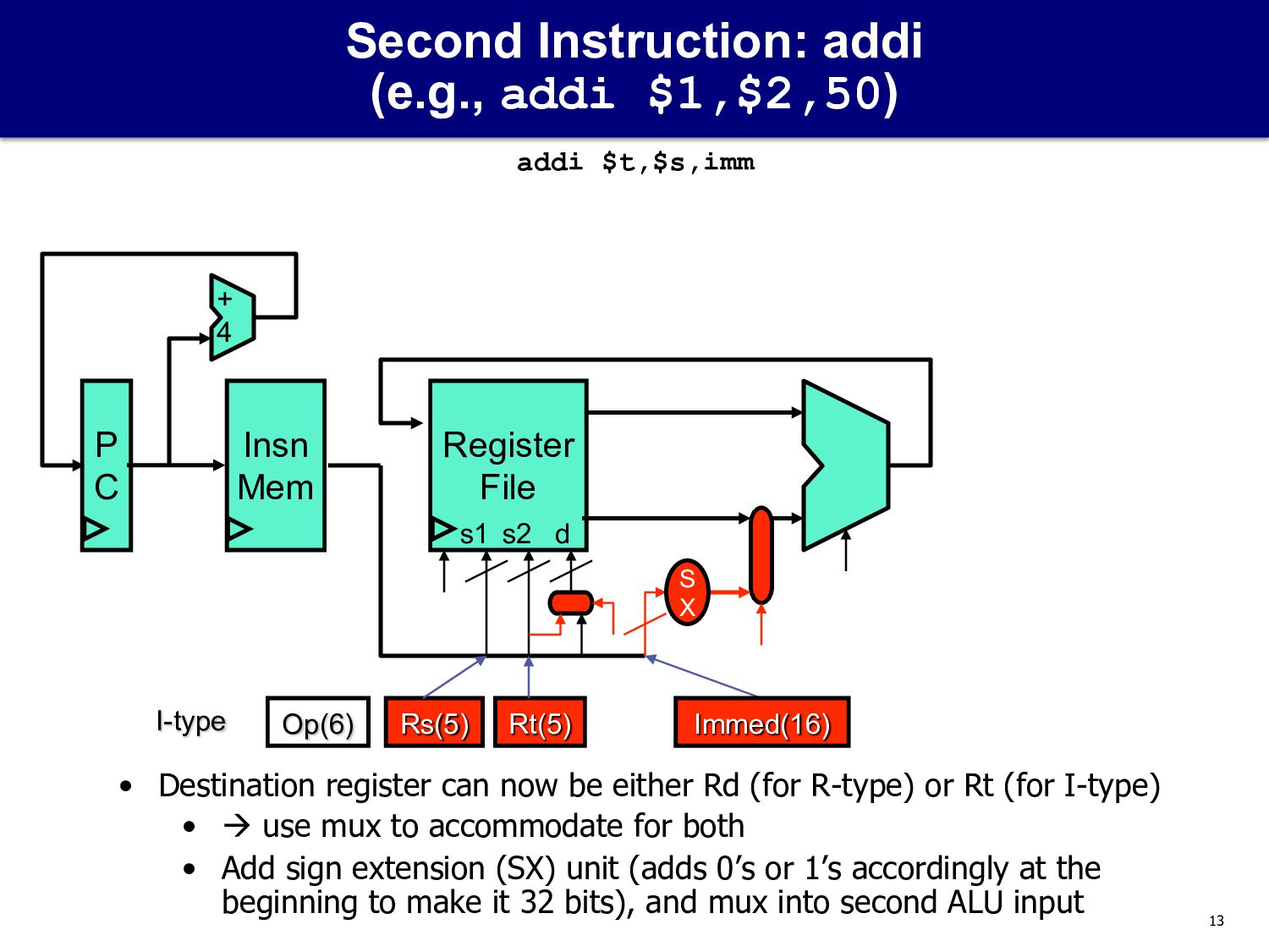
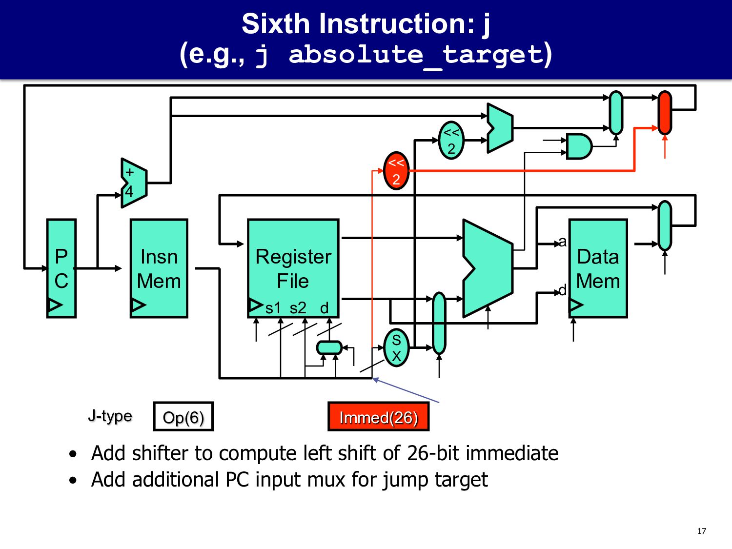
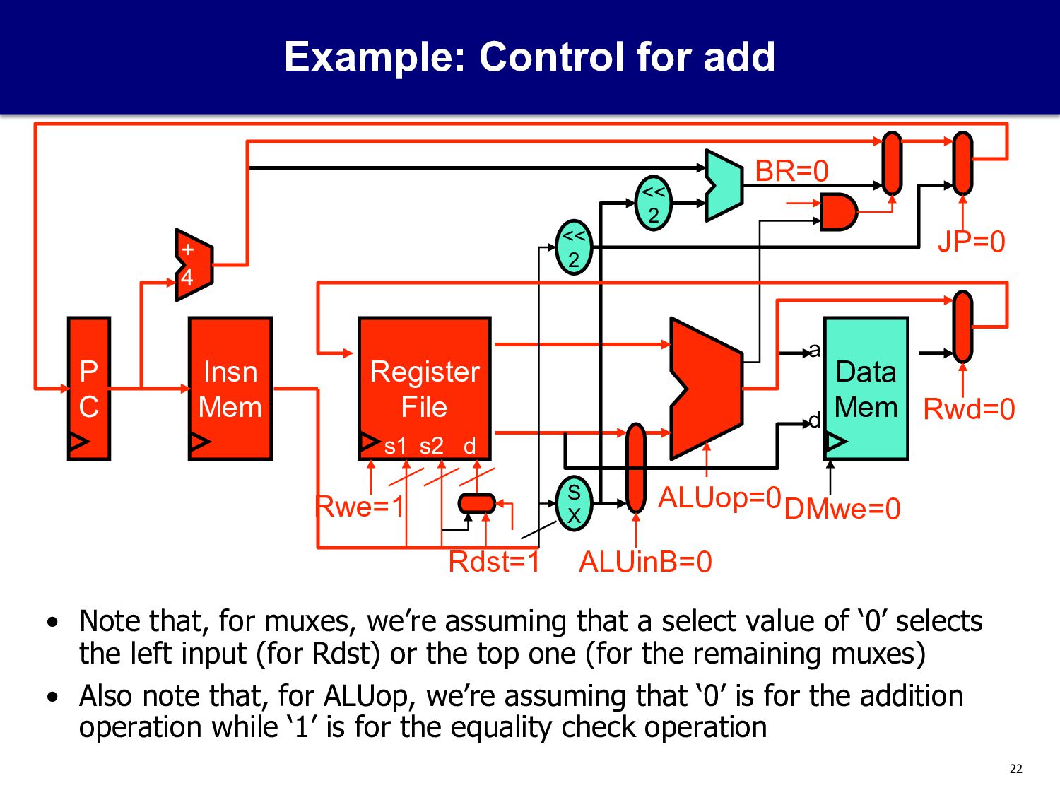
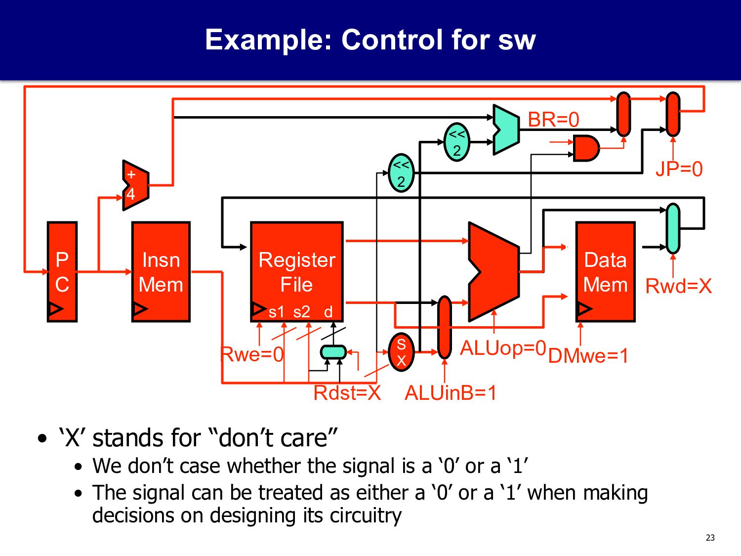
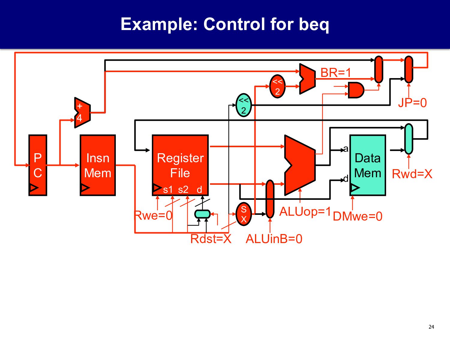
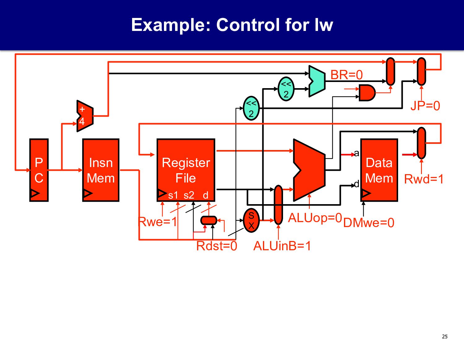
    can now be either Rd (for R-type) or Rt (for I-type) • à use mux to accommodate for both • Add sign extension (SX) unit (adds 0’s or 1’s accordingly at the beginning to make it 32 bits), and mux into second ALU input P C Insn Mem Register File S X Op(6) Rs(5) Rt(5) I-type Immed(16) s1 s2 d + 4 addi $t,$s,imm
  3. 14 Third Instruction: lw (e.g., lw $1,4($3)) • Add data

    memory, address is ALU output • Add register write data mux to select memory output or ALU output P C Insn Mem Register File S X Op(6) Rs(5) Rt(5) I-type Immed(16) s1 s2 d Data Mem d + 4 a lw $t,imm($s)
  4. 15 Fourth Instruction: sw (e.g., sw $1,4($3)) • Add path

    from second input register to data memory data input P C Insn Mem Register File S X Op(6) Rs(5) Rt(5) I-type Immed(16) s1 s2 d Data Mem a d + 4 sw $t,imm($s)
  5. 16 Fifth Instruction: beq (e.g., beq $1,$2,PC_relative_target) • Add left

    shift unit and adder to compute PC-relative branch target • Add PC input mux to select PC+4 or branch target • Note that shifting by a fixed amount is very simple (doesn’t need additional logic components) P C Insn Mem Register File S X Op(6) Rs(5) Rt(5) I-type Immed(16) s1 s2 d Data Mem a d + 4 << 2 eq
  6. 17 Sixth Instruction: j (e.g., j absolute_target) • Add shifter

    to compute left shift of 26-bit immediate • Add additional PC input mux for jump target P C Insn Mem Register File S X Op(6) J-type Immed(26) s1 s2 d Data Mem a d + 4 << 2 << 2
  7. 18 Practice with More Instructions • Pick other MIPS instructions

    and contemplate how to add them • jal (J-type) • jr (R-type) • … P C Insn Mem Register File S X s1 s2 d Data Mem a d + 4 << 2 << 2
  8. 19 d Datapath Timing • Works because writes (PC, RegFile,

    DMem) are independent • We’ll discuss data dependencies later P C Insn Mem Register File S X s1 s2 d Data Mem a + 4 Read IMem Read Registers Read DMEM Write DMEM Write Registers Write PC
  9. 21 d What Is Control? • 8 signals control flow

    of data through this datapath • MUX selectors, or register/memory write enable (“we”) signals • A real datapath has hundreds of control signals P C Insn Mem Register File S X s1 s2 d Data Mem a + 4 << 2 << 2 Rwe ALUinB DMwe JP ALUop BR Rwd Rdst
  10. 22 Example: Control for add • Note that, for muxes,

    we’re assuming that a select value of ‘0’ selects the left input (for Rdst) or the top one (for the remaining muxes) • Also note that, for ALUop, we’re assuming that ‘0’ is for the addition operation while ‘1’ is for the equality check operation P C Insn Mem Register File S X s1 s2 d Data Mem a d + 4 << 2 << 2 BR=0 JP=0 Rwd=0 DMwe=0 ALUop=0 ALUinB=0 Rdst=1 Rwe=1
  11. 23 Example: Control for sw • ‘X’ stands for “don’t

    care” • We don’t case whether the signal is a ‘0’ or a ‘1’ • The signal can be treated as either a ‘0’ or a ‘1’ when making decisions on designing its circuitry P C Insn Mem Register File S X s1 s2 d Data Mem a d + 4 << 2 << 2 Rwe=0 ALUinB=1 DMwe=1 JP=0 ALUop=0 BR=0 Rwd=X Rdst=X
  12. 24 d Example: Control for beq P C Insn Mem

    Register File S X s1 s2 d Data Mem a + 4 << 2 << 2 Rwe=0 ALUinB=0 DMwe=0 JP=0 ALUop=1 BR=1 Rwd=X Rdst=X
  13. 25 Example: Control for lw P C Insn Mem Register

    File S X s1 s2 d Data Mem a d + 4 << 2 << 2 BR=0 JP=0 Rwd=1 DMwe=0 ALUop=0 ALUinB=1 Rdst=0 Rwe=1
  14. 26 d How Is Control Implemented? P C Insn Mem

    Register File S X s1 s2 d Data Mem a + 4 << 2 << 2 Rwe ALUinB DMwe JP ALUop BR Rwd Rdst Control Circuit opcode
  15. 31 “Single-Cycle Datapath” Performance • Goes against make common case

    fast (MCCF) principle + Low Cycles Per Instruction (CPI): 1 – Long clock period to accommodate the slowest insn d P C Insn Mem Register File S X s1 s2 d Data Mem a + 4 << 2 << 2 Rwe ALUinB DMwe JP ALUop BR Rwd Rdst Control Circuit opcode