Upgrade to Pro — share decks privately, control downloads, hide ads and more …

Benchmarking Josephson Junctions for Scalable Quantum Computing - Report

Alexa Jakob
May 27, 2022
130

Benchmarking Josephson Junctions for Scalable Quantum Computing - Report

Alexa Jakob

May 27, 2022
Tweet

Transcript

  1. Benchmarking Josephson Junctions at Room Temperature Senior Project Report -

    ECE 396 May 27, 2022 Group Members: Tamar Bacalu Alexa Jakob Mark Koszykowski Abstract Quantum computing has the potential to revolutionize every industry by allowing scientists to run com- putations for a class of problems which are inaccessible for classical computers. One way to create qubits is to use Josephson Junction Field Effect Transistors (JJFETs), which take on quantum properties only at cryogenic temperatures on the order of millikelvin. Bringing the devices to low temperatures for verification is time-consuming and expensive, and as quantum computing continues to grow, efficient verification will become even more difficult and even more important. Wanting to make the verifica- tion process easier, in this project, we build on the Shabani Lab’s research studying the fabrication of quantum devices. We simulate and measure voltage and current characteristics at room-temperature for a preselected device. We advance the characterization process towards determining whether there exists a general mathematical relationship between a device’s characteristics at room temperature and at cryogenic temperatures, which would allow for faster and cheaper verification of future JJFETs. Introduction Semiconductor manufacturers already have the resources to programmatically characterize processors ef- ficiently at room temperature, but these methods do not yet exist at cryogenic temperatures. This makes it difficult to determine whether fabricated qubit processors will pass validation specifications without checking each individual qubit, and hinders the scalability of quantum processors. Unlike traditional silicon transistors, InAlAs transistors exhibit classical behavior at room temperature and quantum behavior when cooled to cryogenic temperatures (on the order of millikelvins (mK)). Our goal is to find classical properties of quantum devices through simulation and measurement, which can provide valuable insight into their quantum behavior by determining a relationship between the room temperature and cryogenic temperature properties of InAlAs transistors, specifically Josephson Junction Field Effect Transistors (JJFETs). In this report, we will provide background information on quantum devices, discuss our simulations and measurements and their results, and share information about the analysis process and potential future work. Background Important Equations Outlined here are fundamental physics equations which are necessary to solve the state of quantum systems. NextNano is an example of software used to solve these equations for a given setup and is the primary simulation software used in this work. 1
  2. Schr¨ odinger Equation The Schr¨ odinger Equation, shown in equation

    (1), is often used in quantum mechanics to help predict the future behavior of a dynamic system. It is written in terms of the wavefunction Ψ, which when multiplied by its conjugate demonstrates the probability that a particle is at some location at some time. [ −¯ h2 2m ∇2 + V (r, t)]Ψ(r, t) = i¯ h ∂ ∂t Ψ(r, t) (1) Because of the nature of the equation, the left hand side is modelled as a Hamiltonian operator ( ˆ H) which helps generate the evolution of the waveform in time. This simplification allows the wavefunction to be an eigenfunction and the energy of the system E to be the eigenvalue, demonstrated in equation (2). (9) ˆ HΨ = EΨ (2) Poisson Equation The Poisson Equation, shown in equation (3), is often used to determine the electric potential at a point in space based on the charge density that caused it. It is derived from Gauss’ Law of electric flux and the standard relationship between an electric field and the electric potential. (8) ∇2V = −ρ ϵ0 (3) Temperature Dependence of Materials Metals Metals, also known as conductors, have no energy gap between the conduction and valence bands. There- fore, when a current is applied, these electrons on the outer most band are free to move within the structure. When temperature increases, the lattice structure in the material begins to vibrate with a higher ampli- tude. This larger vibration leads to more collisions which drain energy from the free electrons making them move, or flow, at a slower drift velocity. This all means that as temperature increases, mobility of electrons decreases, meaning that conductivity decreases and resistivity increases. (1) Insulators In nonmetals, also known as insulators, there is a very high energy gap between the valence band and conduction band. This means that there must be a very large energy applied to the material for a valence electron to move to the conduction band. When temperature increases, the lattice of the material begins to vibrate with a higher amplitude which will cause electrons in the valence band to absorb energy and move to the conduction band. This all means that as temperature increases, the mobility of electrons increases, meaning that conductivity increases and resistivity decreases. (1) Semiconductors A high temperature of semiconductors will increase their conductivity, because a small amount of heat will excite electrons enough for them to become free and jump to the conduction band. However, doping is a more reliable way to induce this current. In semiconductors, the valence band of the atoms are full which in general prevents the flow of electrons. However, if enough energy is applied, electrons in the valence band can be excited enough to enter the con- duction band, resulting in a hole in the valence band. This excitation can be achieved through temperature manipulation or by doping. The conductivity, which is inversely proportional to resistivity, for semiconductors is given by the following equation: σ = q(µn n + µp p) (4) 2
  3. Where µ represents carrier mobility and n and p represent

    electron and hole concentration respectively. Each component of this equation has its own dependence on temperature. For carrier mobility, there are two main effects which influence it: lattice scattering and impurity scattering. Lattice scattering is when lattice vibrations cause the mobility to decrease. These vibrations are correlated to temperature, since temperature is average kinetic energy, and therefore as temperature increases the mobility due to lattice scattering decreases (T−3/2 dependence). Impurity scattering is caused by impurities in the material, and when temperature decreases, carriers move more slowly, decreasing mobility (T3/2 dependence). While total mobility is equal to the sum of the two, impurity scattering is typically only seen at very low temperatures. Intrinsic carrier concentration (ni ) is related to temperature by a T3/2exp( 1 T ) relationship where generally the exp( 1 T ) component is said to dominate. However, the total charge concentrations of electrons and holes are given by the following equations: n(T) = N+ D (T) − N− A (T) + ni (T)2 n(T) (5) p(T) = N− A (T) − N+ D (T) + ni (T)2 n(T) (6) At very low temperatures, ni is very small and the donor electrons are bound to the donor atoms. This is called ionization. At high temperatures, ni dominates and carrier concentration increases with temperature (known as the intrinsic region). In between these two, a change in temperature will result in no change in carrier concentration, which is known as saturation (or the extrinsic region). Because of these two factors, there is no one relationship that explains the relationship between tempera- ture and conductivity of a semiconductor. For example, with one doping scheme, impurity scattering may be dominant at low temperatures and carrier concentration is determined by extrinsic doping so conductivity would increase, and resistivity would decrease, as temperature increases. However, with another doping scheme, if carrier concentration is intrinsic and mobility is dominated by lattice scattering, conductivity would decrease, and resistivity would increase, as temperature increased. (3) Josephson Junctions Calculating the supercurrent of a Josephson Junction A Josephson Junction is a device consisting of an insulator or non-superconducting material sandwiched between two superconducting layers. This device can also be modeled as a nonlinear inductor in parallel with a capacitor. The nonlinearity of the inductor allows the formation of a two-level quantum system. Typically, current would not be able to travel through the insulator, but quantum mechanically the electrons can tunnel through the insulating barrier with a supercurrent and zero voltage. This current is also called the Josephson current, and the phenomenon where the wavefunction (and cur- rent) propagates through the barrier is known as quantum tunneling. Because of this phenomenon, one can use Schrodinger’s equation to determine the wavefunction of the electrodes and calculate the supercurrent going through the Josephson Junction (as well as its current-phase relation in the presence of an electromag- netic field). The supercurrent is calculated to be the critical current multiplied by the sine function of the phase difference of the wavefunctions of two superconducting electrodes. The critical current is the maximum DC current permitted through the junction before it stops superconducting, measured at the point where the voltage jumps from zero to some finite value. (2) Relationship between superconductor gap and supercurrent A JJFET has some width w and some gap length l, demonstrated in Figure 1. The w l ratio will determine the amount of current the junction is able to produce. In the ballistic regime, we have the equation Ic Rn = α∆ e , where ∆ e is a normalization factor and α represents the gap l between semiconductor and superconductor. By rearranging this equation, we get Ic ∆ = αRn e . Since Rn depends on the geometry of the junction (Rn = ρ l A , where ρ is the resistivity of the 3
  4. Figure 1: Superconductor Gap (left) as seen on a JJFET

    (right) material, l is the length of the isolation portion, and A is the cross-sectional area of the junction), this means that the critical current can be controlled by the values of w and l. (7) Ballistic and Diffusive Modes A JJFET has three significant lengths that contribute to its properties: the mean free path in the semicon- ductor (le ), the superconducting coherence length (ξ0 ), and the junction length (L). Two of these properties in relation dictate whether a JJFET is in the ballistic or diffusive regime. This distinction is important because being in these two different regimes has different implications on the relation between the normal resistance (RN ) and the critical current (IC ). A ballistic transparent junction will relate the two through the following IC RN = π ∆0 e whereas a diffusive transparent junction will do so through IC RN = 1.32π 2 ∆0 e . A junction will be deep in the ballistic regime if le >> L, but deep in the diffusive regime if L >> le . These properties are not only determinable by means of these two characteristics, but by comparing the relation between the normal resistance and critical current. For example, for a JJFET with a L = 100nm and le = 87nm, if the relation between the critical current and normal resistance exceeds that of a diffusive junction, then it would be described as short ballistic, since the junction does not fall deeply into either regime. (11) Project Description The goal of this project is to help determine a mathematical relationship between quantum device char- acteristics at room and cryogenic temperatures. The three main properties of interest that are insightful to this study are the resistance R, normal resistance RN and critical current IC . The resistance refers to the resistance of a device at room temperature. The normal resistance is the non-zero resistance of a device at cryogenic temperatures when the device has exited the superconducting state. The critical current is the maximum amount of current that a superconducting quantum device can sustain at cryogenic temperatures before exiting the superconducting state, and thereby losing its quantum properties. This quality is very important in determining the usability of devices because JJFETs will often be used in a gatemon qubit con- figuration, and the device’s critical current has an impact on the device’s resonant frequency which changes the qubit’s behavior. While some general relations between two of the three properties are known for some devices as explained in the background, the ballistic or diffusive distinction is not necessarily discrete. Often times, the determination of such classifications are a result of studying the device’s normal resistance and critical current, if the device does not heavily favor either class. However, this determination still requires bringing devices down to superconducting temperatures, which this work helps to alleviate. 4
  5. Our goal is to study a specific, desirable materially structured

    JJFET and help lay the groundwork to determine this relationship. Properties of the device at cryogenic temperatures are known, however its properties at room temperature are an anomaly. The first step in this process is to conduct simulation work to get an idea of what the expectation is. Strides have been made to first replicate the results that have been produced at the lab already to ensure our theoretical work is on the right track. Our goal is to increase the dimensions of these simulations to construct a more accurate model. Once this was completed we began simulating at room temperatures in order to help those in the future develop a theoretical mathematical foundation. Altogether, this could save manufacturing and testing time and make it easier to scale quantum computers. Design and Implementation Procedure JJFET Structure The JJFET used to conduct the simulations needed to calculate the mathematical model is shown in Figure 2. From left to right, the contact points are three metals that correspond to the source, gate, and drain. The superconducting material that is sandwiching the insulator in this JJFET is Indium Gallium Arsenide, and Indium Arsenide is the nonsuperconduting material used as the insulator. The dopant silicon is used as the sheet charge and the substrate region is made up of Indium Phosphide which is a binary superconductor composed of both indium and phosphorus. (10) Figure 2: Material Stack of JJFET studied in this work The physical structure of the JJFET studied in this work resembles that of one shown in Figure 3. The device is symmetric vertically (in this figure) around the gate which is highlighted in yellow on the left. The four gray corners represent the contacts for the source (two on the left) and drain (two on the right), or vice versa since the device is symmetric. It is important to note though that the material stack shown in Figure 3 is not the same as the device studied here. 5
  6. Figure 3: Physical model of JJFET showing where the material

    stack is present (red highlighten box is top-down view of material stack) (10) Simulation and Results NextNano NextNano is simulation software that allows the user to design and simulate electronics at a nano scale using both quantum and classical methods. Shabani Lab uses this software to simulate its devices. In our project, we are using NextNano to determine IV curves of the device and electron density of the quantum well. Sample simulations are provided in Appendix A. Results One Dimensional All current results are from simulating the desired JJFET (shown in Figure 2) at room temperature, more specifically 300K. Figure 4 shows a simulation conducted using a one dimensional representation of the JJFET, taken as a cross section down the middle of the gate pin: lower x values represent material listed higher in Figure 2. As expected, the electron density peaks at the quantum well (InAs). This is a direct effect of the insulating nature of the well which does not allow the flow of electrons, causing electrons to get trapped in the well. This higher electron density also gives it a lower charge as expected and as shown. Figure 5 represents the electron density of the quantum well as the gate voltage of the device is swept, simulated in one dimension. As the voltage increases, there is a larger electric field causing more electrons to flow and thus more getting trapped in the well. The figure demonstrates two approximately linear regions, one from approximately V = −1V to V = 7.5V and one from V = 7.5V and greater. These two linear regions represent the two subbands of the InAs getting filled with negative charge. The first subband can only sustain a limited critical density, at which the second subband of the molecules start getting filled, hence the change in rate of electron density. 6
  7. Figure 4: 1 dimensional electron density across stack at room

    temperature Figure 5: 1 dimensional critical density in InAs at room temperature Two Dimensional The same experiment of gate sweeping was replicated in two dimensions, this is shown in Figure 6. A much smaller range of values were swept for the domain as a result of the significant increase in computational time and complexity of bumping up the dimensionality. Figure 7 demonstrates another two dimensional simulation conducted. Here, the current drawn through the source and drain pins were measured. As expected, since no current is lost to tunneling because tests were conducted at room temperature, there is a consistent increase and decrease of current in the drain and source, respectively. Figures 5 and 6 were simulated with a simplified version of the 2D structure, due to errors in the NextNano simulation. Future work will involve refining the structure to refer more exactly to existing devices the lab has manufactured. 7
  8. Figure 6: 2 dimensional electron density in InAs at room

    temperature Figure 7: 2 dimensional current through source and drain at room temperature Instruments and Software All measurements were performed at New York University’s Center for Quantum Phenomena. Various existing chips were measured. Each chip has multiple JJFET devices and is mounted to a daughterboard, a circuit board that connects transistor pads to external pins, to allow for simpler integration with their quantum computer. For our purposes, we probe the pads of the device directly to get a more accurate measurement of device specific properties. The instruments and software used are as follows. Probe Station The chip is placed on the platform of the device shown in Figure 8, which is a probe station designed for small-scale devices. A chuck pump suctions the chip to the platform and prevents it from moving. The probe 8
  9. station offers movement of the platform in all three spatial

    dimensions, along with rotational capabilities. Additionally, it contains a built in microscope to allow for accessible viewing of the probed device, a depiction of the microscope view is displayed in Figure 9. There are four pins connected to coaxial cables that run to measurement instruments shown in Figure 10. Figure 8: Unloaded probe station Figure 9: View of JJFET (JS129A) under microscope 9
  10. Keithley 2400 & Keithley 2450 Figure 10: Instruments used for

    measurements The Keithley 2400 (4) and Keithley 2450 (5) are incredibly accurate source meters able to source voltage and measure current and voltage, all simultaneously. They allow for precise limiting of outputted current or voltage, and are fully controllable remotely using computer software. These were used to voltage bias the gate and source of tested devices while taking measurements of current at both terminals. Labber Labber (Keysight) is software provided by Keysight that allows scientists to automate measurements using their instruments. Labber was used to set up measurements, sweep the appropriate terminals, collect data, and explore the data using its graphical tools. Labber allows to save configurations to alleviate the stress of setting up the exact same tests. Addition- ally, Labber outputs collected data to hdf5 files for easy analyze through programming languages such as MATLAB or Python. MATLAB code used in this work for visualization can be seen in Appendices B, C, and D. Measurements Gate Test The gate of a JJFET is very fragile since it is the thinnest layer. It is most susceptible to becoming detached from the rest of the device and can be damaged by relatively large currents, which can cause current leakages. Therefore, before taking a measurement to determine desired characteristics, we must ensure that the gate is in good condition. This is done by performing a gate test, a schematic for which is shown in Figure 11. In a gate test, the gate voltage (VG ) is slowly sweeped while monitoring its current. As soon as the gate current reaches levels suggesting a leakage, the measurement is stopped and the gate voltage (VG ) is immediately and gradually lowered to zero in order to preserve the gate condition. A normal gate current is on the order of picoamperes (pA); once the current reaches hundreds of picoamperes (pA) or even nanoamperes (nA), that gate voltage (VG ) is deemed out of range for future testing. A gate test was often conducted in multiple parts over different domains in order to ensure the protection of its stability. This process may be repeated, sweeping in both increasing and decreasing gate voltage (VG ) in order to determine an acceptable gate voltage (VG ) range for this specific device in future measurements. 10
  11. Figure 11: Schematic of gate test measurement Sweeping Source Voltage

    biasing the source while keeping the gate and drain at a constant voltage allows for measuring the evolution of the current through the device as quantity VSD changes at room temperature. Using Ohm’s Law, V = IR, the resistance of the device can be calculated as the inverse of the slope of the graph of source current as a function of source-drain voltage. Our expectation, in alignment with Ohm’s law, is for the relationship between voltage and current to be linear for some small voltage domain tested. Therefore as the source-drain voltage increases, so should the source current. Sweeping Gate Increasing the gate voltage (VG ) increases the number of carriers (i.e. electrons) present in the channel. Sweeping the gate voltage (VG ) for a given source-drain voltage bias allows for deeper analysis by showing how the resistance of a device changes for each gate voltage (VG ) value. During this measurement, we must be careful to sweep the gate very slowly (around 100mV s ) and to remain within the safe range determined by a previously performed gate test. As a result of increasing the gate voltage (VG ), we generally expect the resistance to decrease as more carriers are added to the channel. A schematic of the set up used to measure the resistance (R) at room temperature by sweeping the gate and source-drain voltage can be seen in Figure 12. To model the JJFET as a resistor, the following schematic can be drawn, as shown in Figure 13. There are a couple important things implied by this schematic. First of all, The resistance that would be calculated from the proposed setup is not the resistance of the isolated JJFET since there is also resistance from the instrumentation and the contacts of the device connected in series. Additionally, since the resistance (R) is expected to change as a function of gate voltage (VG ), each new gate voltage (VG ) would implement a new resistor with a different resistance in this schematic. 11
  12. Figure 12: Schematic of resistance measurement by sweeping gate (VG

    ) and source-drain (VSD ) voltage R1 Rwire R2 Rpin R3 Rwire R4 Rpin R5 Rpin R6 Rpin R7 Rwire R8 Rwire R9 Rjunction Source Source Drain Drain K2450_Vsource K2450_Imeas Aluminum Indium Arsenide --- C:\Users\Alexa Jakob\OneDrive\Documents\Cooper Year 4\Senior Project\sourcesweep.asc --- Figure 13: Equivalent resistance schematic of sweeping source-drain voltage (VSD ) for a given gate voltage (VG ) Contact and Instrumentation Resistance To measure the correct resistance of only the junction, the contact resistance and the instrumentation resistance needs to be measured in order to subtract it from the total resistance measured. The instru- mentation resistance is the resistance of the contacting interfaces of the coaxial cables and the probe pins. It is measured by supplying a voltage onto one pad of the source or drain, and measuring the current on the same pad with another cable and pin. Using the equation V = IR, we can divide the voltage by the current to retrieve the resistance of both the cables and the pins on the pad. The setup for measuring the instrumentation resistance is in figure 14 below. An equivalent schematic with the JJFET modeled as a resistor is shown in Figure 15. The contact resistance is the resistance between the pads of the device that should also be subtracted from the total measurement resistance. It is measured similarly to how the instrumentation resistance is measured except it is done by probing the two pads of either the source or drain, instead of one. This setup can be seen in Figure 16. Ideally the contact resistance would be measured in order for the true device resistance to be calculated, however this was not accomplished in this work. 12
  13. Figure 14: Instrumentation resistance measurement setup R1 Rwire R2 Rpin

    R3 Rwire R4 Rpin R5 Rpin R6 Rpin R7 Rwire R8 Rwire R9 Rjunction R10 Rwire R11 Rpin Source Source Drain Drain K2450_Vsource K2450_Imeas Aluminum Indium Arsenide --- C:\Users\Alexa Jakob\OneDrive\Documents\Cooper Year 4\Senior Project\contactR.asc --- Figure 15: Equivalent resistance model of measuring instrumentation resistance Figure 16: Contact resistance measurement setup Setbacks Outlined below are some of the difficulties that were encountered while taking these measurements. These setbacks explain the testing of only a single device and may prove as informative to those studying this 13
  14. mathematical relation in the future. Instrumentation Instrument malfunction was the

    most common cause of setbacks throughout the measurement process. In order to guarantee good data, the measurement process always began with checking each instrument before connecting them to the device. Checking these instruments included sending out a correct signal, maintaining a steady output, and reading a correct signal, for both voltages or currents. Unfortunately, the instruments do not always behave ideally. At one point, the Keithley 2400 that was used to measure the source-drain voltage was not working properly and was measuring its own output rather than what was supplied to it. To get around this setback, an attempt was made to supply voltage using the 2400 and measure the current using the 2450. This setup was not effective either since the 2450 would not measure current. To circumvent this issue, different instruments were used. Incorrect Biasing Initial measurements were done by current biasing the device, which involved sending current to the source using a voltage source with a large resistor (on the order of megaohms (MΩ)) in series, since this resistance was assumed to be far larger than that of the device, and measuring the voltage difference of the source and drain. The measurements done at cryogenic temperatures were done using current biasing, which is why this measurement was also chosen at room temperature. However, it was understood much later that voltage biasing was the proper approach in order to measure the resistance. Voltage biasing involves applying a voltage to the source and measuring current at the source while grounding the drain, the opposite of initial attempts. In classical semiconductor devices, current biasing does not affect the voltage meaningfully, and this is not a common transistor characteristic. The voltage bias characteristic is often used in industry and provides better results. Probe and Pads The biggest and most prevailing setback occurred as a result of incorrect connections to the devices. First, although the source and drain are interchangeable, there are two source and drain pads each. The device is axially symmetric about the gate, and it is essential to connect to the correct pads. In the beginning, it was mistakenly thought that the device was axially symmetric about the incorrect axis. The probe station is quite sensitive and its needles are already bent. As a result, pressing the needles further into the device does not necessarily result in a better connection, as the tips of the needles bend back up away from the device and do not touch the pads with the desired pressure. Since establishing a good electrical connection was essential to get a good measurement, patience and caution are required. This was a major source of measurement error early on. Since the devices were fabricated several years ago, a thin layer of oxide has formed on top of the source and drain pads. This is normal; however, this was not known until a researcher from NYU Tandon, Zhujun Huang, was able to obtain good data in her laboratory after making this observation. Going forward, the oxide from the device’s pads was scratched off delicately using the probing station pins, being sure to not damage the device, and a good electrical connection was ensured and tested before setting up automated sweeps. Measurement Results All results included in this section were obtained from measurements performed on the JJFET labelled JS129A at the Shabani Lab. 14
  15. Gate Test Figure 17 includes an example of a gate

    test performed: the different colors represent separate consecutive tests that were run. The initial current spike (around ∼ 770mV ) is considered to be an anomaly since the current increases sharply but quickly recovers. There is leakage current present around 900mV , as the current increases for several consecutive points. At that point, the measurement was stopped and the gate was incrementally returned to zero volts. Figure 17: Gate test results Sweeping Source Figure 18 demonstrates the results of sweeping the voltage applied to the source (VSD ) while holding the gate voltage (VG ) constant. Seeing as good electrical contacts were made and the gate voltage was maintained in the safe range as determined by the gate test demonstrated in Figure 17, clean data was acquired. Since the sweep of the voltage was kept between a small range, more specifically in the linear range, a linear relation between source-drain voltage and source current was obtained. -1 -0.5 0 0.5 1 -8 -6 -4 -2 0 2 4 6 8 Figure 18: Voltage bias measurement for one gate voltage value (VG = 200mV ) 15
  16. Sweeping Gate and Source Sweeping the gate voltage (VG )

    while sweeping the source-drain voltage VSD provides insight to how the slope (related to resistance (R)) changes due to different gate voltages. It was already expected that there would be a linear relation between the source-drain voltage (VSD ) and source current (IS ), as shown in Figure 18. Figure 19 demonstrates the results of simultaneously sweeping VSD and VG . The gate voltage (VG ) was swept from −500mV to 500mV , where both ends of the gate voltage (VG ) domain had the steepest slope, and the most gentle slope occurred when VG was 0mV . Generally, as the magnitude of the gate voltage (VG ) increased from 0V , the slope became steeper, signifying a decrease in the resistance of the device. There was one anomaly that occurred while measuring when VG was 100mV , which is likely a result of movement of the setup or device which can disrupt the electrical connection. -1 -0.5 0 0.5 1 -8 -6 -4 -2 0 2 4 6 8 Figure 19: Simultaneous sweep of gate (VG ) and source-drain (VSD ) voltage Calculations Resistance at Room Temperature According to Ohm’s law, V = IR, and therefore R = V I . The resistance is the inverse of the slope of the linear curve obtained. In order to account for instantaneous variations in the resistance of the device since it is inherently nonlinear, the partial derivative of the curve at every instant with respect to source-drain voltage was approximated using the following calculation: ∂IS ∂VSD ≈ IS (n + 1) − IS (n) VSD (n + 1) − VSD (n) (7) Using this discretized calculation, Figure 20 was obtained. 16
  17. Figure 20: Instantaneous resistance of total setup with simultaneous sweep

    of gate (VG ) and source-drain (VSD ) voltage However, there must also be some resistance from the instrumentation with the probe station. This is measured with the instrumental resistance measurement setup displayed in Figure 14. The results from this measurement are shown in Figure 21. This measurement also includes some of the resistance within the pad the probes were on as well as the pins and wires of the probes themselves. The contact resistance is the resistance through the pads to the device that should have been measured. These measurements were not taken, so they were neglected. Ideally these measurements would be taken by connecting the two probes to both the source pins or both the drain pins and subtracted from the total resistance to get the true resistance of the device. -0.25 -0.2 -0.15 -0.1 -0.05 0 0.05 0.1 0.15 0.2 -0.04 -0.03 -0.02 -0.01 0 0.01 0.02 0.03 Figure 21: Measurement of instrumentation resistance results 17
  18. Ideally, the results of the instrumental resistance test would be

    perfectly linear, representing a constant nonzero resistance of the instrumentation. This was almost achieved as shown in a full graph in Figure 22 with demonstrates the instantaneous slope of the measurements in Figure 21, a zoomed in version of which is shown in Figure 23. -0.2 -0.15 -0.1 -0.05 0 0.05 0.1 0.15 0.2 0.25 -300 -200 -100 0 100 200 300 400 Figure 22: Instrumentation resistance with respect to voltage -0.2 -0.15 -0.1 -0.05 0 0.05 0.1 0.15 0.2 0.25 -20 -15 -10 -5 0 5 10 15 20 Figure 23: Zoomed in instrumentation resistance with respect to voltage 18
  19. The median instrumentation resistance was found to be 7.08Ω. The

    median was used due to the large presence of outliers with the underlying assumption that the resistance of the instrumentation was indepen- dent of the voltage applied to it. With the assumption that the instrumentation resistance is independent of gate voltage (VG ) and would remain constant over all tested values for which, the contact resistance was subtracted from the total measurement resistance to obtain the device’s upper limit resistance. Ideally, the contact resistance would have also been measured, creating a greater resistance to be subtracted. Therefore, the resistance value that we calculated is used as an upper limit of the device resistance. A two dimensional heatmap of just the device’s upper limit resistance is demonstrated in Figure 24. Figure 24: Instantaneous resistance of just the device with simultaneous sweep of gate (VG ) and source-drain (VSD ) voltage Due to the significant amount of inconsistencies in the data was were a result of the faulty measurement when VG = 0.1V , those results were excluded from further visualizations of this experiment to allow for more accurate but less precise results. The upper limit of the device’s resistance without the excessive noise is shown in Figure 25. The upper-limit of the final resistance for the device was found to be 156.72Ω. The relationship between the resistance (R) and gate voltage (VG ) is displayed in Figure 26. There is a significant spike in the resistance (R) when VG = 0.1V . This is likely a result of temporary poor electrical connection as a result of movement, which led to a significant increase in the observed resistance of the device. . 19
  20. Figure 25: Instantaneous resistance of just the device with simultaneous

    sweep of gate (VG ) and source-drain (VSD ) voltage, removing VG = 0.1V due to extreme perturbation -0.5 0 0.5 130 140 150 160 170 180 190 200 210 220 230 Figure 26: Relationship between resistance (R) and gate voltage (VG ) of JS129A Resistance in Cryogenic Temperatures In order to be measured at cryogenic temperatures, a device must be carefully cooled inside a dilution refrigerator, the one located at New York University’s Shabani Lab can be seen in Figure 27. Each layer, from top to bottom, becomes progressively colder, and the sample sits at the bottom, where the coldest temperature is achieved. Cryogenic measurements for JS127A were taken by Ph.D. students at the Shabani lab in 2019 and can be seen in Figure 28. These measurements differ from the methodology used here in several ways. First, the temperature difference is significant. Here, samples are measured at room temperature (about 294K), while samples in the quantum fridge are cooled down to several millikelvin (mK). Second, at low temperatures, it is possible to use a wider range of gate voltage (VG ) values. Figure 28 uses gate voltages as low as −32V , which 20
  21. Figure 27: One of the dilution refrigerators at the Center

    for Quantum Phenomena at New York University would be impossible for this device at room temperature since it would result in a large leakage current. Finally, the cryogenic measurements were current biased, whereas the measurements taken in this study were voltage biased. As a result, there may be some different behavior, even though the exact parameters of measurement may differ. The graph provided in Figure 28 is in fact not the exact same chip that was used for room temperature benchmarking, but rather a JJFET that utilized a very similar material structure. Due to inconsistencies about exact chips, as well as confusion about the methodology of measurement, no quantitative analysis is done here. The most important thing to note is the transition from a constant resistance observed for each gate voltage (VG ) at room temperature to a nonlinear normal resistance at superconducting temperatures. However, this may simply be a result of the larger domains of gate voltage (VG ) and source current (IS ) swept. 21
  22. Figure 28: Cryogenic temperature measurements of JS127A Conclusion The goal

    of this work set out to determine a method for room temperature benchmarking of JJFETs to allow for quicker, easier, and less expensive verification in the future. What has been accomplished is the development of sound simulations that accurately depict what is expected to occur in a JJFET. Furthermore, interesting properties about the room temperature resistance of JJFETs have been observed which confirmed many hypotheses that researchers had. The research here lays the groundwork for future work on this topic and the attempt to develop a mathe- matical relation between room temperature and cryogenic properties. Many challenges were overcome which helps those in the future curious about this exploration. With a clear pattern observed in room tempera- ture resistance, there is strong reason to believe that in the future, a mathematical model able to evaluate cryogenic temperature properties of qubits based on room temperature verification is possible. Future Work and Potential Improvements Having only conducted this work in such a short period of time, there were many areas overlooked which leaves a lot of room for future work. Something that was neglected until last minute was the resistance of the contacts of the device which contribute to its measured resistance but do not define the resistance of the JJFET at its core. Measuring this in the future could narrow down the upper limits for devices, which may allow for more accurate models in the the future. Additionally, it would be very useful to sweep a larger range of gate voltages (VG ) since this is possible at cryogenic temperatures and would allow for the development of more accurate relations between the properties at these two temperatures. Using data from a larger domain may give rise to a model that generalizes very well as opposed to overfitting to minute discrepancies which may only be present because of noise. Lastly, a major area of work is to apply this research to more JJFET devices, similar material structures and not. Applying this work to similar material stacks may allow for more transparency about the consistency of the manufacturing of these chips. Attempting this work on different JJFET structures would allow for more generalization about how this approach works and how the desired relation may even pertain to certain physical properties of the device. 22
  23. Acknowledgements Many thanks to the researchers at New York University’s

    Shabani Lab for Quantum Materials and Devices, including Joe Yuan, Mehdi Hatefipour, Zhujun Huang, Billy Strickland, and Javad Shabani. We would like to thank our instructor at the Cooper Union, Neveen Shlayan, as well, and the students in Cooper Union’s past who have helped inspire this project, specifically Aziza Almanakly, Armaan Kohli, and Michael Lendino. 23
  24. References [1] Temperature Dependence of Resistivity. https://www.askiitians.com/iit-jee-electric- current/temperature-dependence-of-resistivity/. [2] (2003).

    Lecture 11: Basic Josephson Junctions. https://web.mit.edu/6.763/www/FT03/Lectures/Lecture11.pdf. [3] Green, P. E. (2011). Temperature Dependence of Semiconductor Conductivity. Technical report, San Jose State University. [4] Keithley. Keithley Model 2400 Series SourceMeter User’s Manual. http://research.physics.illinois.edu/bezryadin/labprotocol/Keithley2400Manual.pdf. [5] Keithley. Keithley Model 2450 Interactive SourceMeter Instrument User’s Manual. https://download.tek.com/manual/2450-900-01 D May 2015 User 3.pdf. [Keysight] Keysight. Labber user Manual. https://www.keysight.com/us/en/assets/9018- 18184/installation-guides/9018-18184.pdf. [7] Mayer, W., Yuan, J., Wickramasinghe, K. S., Nguyen, T., Dartiailh, M. C., and Shabani, J. (2019). Superconducting proximity effect in epitaxial Al-InAs heterostructures. Technical report, New York Uni- versity and University of Maryland and University of New York. [8] Nave, C. R. LaPlace’s and Poisson’s Equations. http://hyperphysics.phy- astr.gsu.edu/hbase/electric/laplace.html. [9] Nave, C. R. Schrodinger Equation. http://hyperphysics.phy-astr.gsu.edu/hbase/quantum/schr.html. [10] Yuan, J. O. (2021). Epitaxial Superconductor-Semiconductor Two-dimensional Systems: A New Plat- form for Quantum Computation. PhD thesis, New York University. [11] Yuan, J. O., Wickramasinghe, K. S., Strickland, W. M., Dartiailh, M. C., Sardashti, K., Hatefipour, M., and Shabani, J. (2021). Epitaxial Superconductor-Semiconductor Two-Dimensional Systems for Su- perconducting Quantum Circuits. Technical report, New York University. 24
  25. Appendix A: Sample NextNano Simulation 1 2 # Simulating a

    1 dimensional JJ at room temperature 3 4 # geometrical parameters in (nm) 5 $width Au = 10.0 6 $width Al2O3 = 30.0 # TODO: should t h i s be SiO2? 7 $width top InGaAs = 10.0 8 $width InAs = 4.0 9 $width bottom InGaAs = 4.0 10 $width InAlAs = 106.0 11 $width InP = 10.0 12 $width si dopant = 1.0 13 $depth si dopant = 6.0 14 15 # other parameters 16 $density si dopant = 3.0 e18 # (cmˆ−3) 17 $density oxide charges = 4.5 e19 # (cmˆ−3) 18 # over 1 nm width t h i s gives a 2D density of 1.0 e12 cmˆ−2. 19 20 # numerical parameters 21 $num subbands = 4 22 $ s p a c i n g v e r y f i n e = 0.025 23 $ s p a c i n g f i n e = 0.1 24 $spacing coarse = 0.4 25 26 $x start Au = −$width Au − $width Al2O3 27 $x start Al2O3 = $x start Au + $width Au 28 $x start top InGaAs = $x start Al2O3 + $width Al2O3 29 $x start InAs = $x start top InGaAs + $width top InGaAs 30 $x start bottom InGaAs = $x start InAs + $width InAs 31 $x start InAlAs = $x start bottom InGaAs + $width bottom InGaAs 32 $ x s t a r t s i d o p a n t = $x start InAlAs + $depth si dopant 33 $x start InP = $x start InAlAs + $width InAlAs 34 $x mid InAlAs = $x start InAlAs + 2.0 $depth si dopant 35 36 37 global { 38 simulate1D {} 39 c r y s t a l z b { 40 41 x hkl = [1 , 0 , 0] 42 y hkl = [0 , 0 , 1] 43 } 44 substrate {name = ”InP”} 45 temperature dependent bandgap = no 46 temperature dependent lattice = no 47 temperature = 300 48 } 49 50 structure { 25
  26. 51 output region index { boxes = yes } 52

    output material index { boxes = yes } 53 output alloy composition { boxes = yes } 54 output impurities { boxes = yes } 55 region { 56 everywhere {} 57 # TODO: should we put dummy contact in InAs or everywhere ? 58 contact { name = dummy } 59 binary {name = ”InP”} 60 } 61 region { 62 # TODO: should we j u s t use Al instead ? 63 l i n e {x = [ $x start Au , $x start Al2O3 ]} 64 contact { name = m e t a l l i c c o n t a c t } 65 # ternary constant { 66 # name = ”In (x) Al(1−x)As” 67 # a l l o y x = 0.81 68 # } 69 } 70 region { 71 l i n e {x = [ $x start Al2O3 , $x start top InGaAs ]} 72 contact { name = dummy } 73 binary { 74 name = ”SiO2” 75 } 76 } 77 region { 78 l i n e {x = [ $x start top InGaAs , $x start InAs ]} 79 ternary constant { 80 name = ”In (x)Ga(1−x)As” 81 a l l o y x = 0.81 82 } 83 } 84 85 region { 86 l i n e {x = [ $x start InAs , $x start bottom InGaAs ]} 87 binary {name = ”InAs”} 88 } 89 region { 90 l i n e {x = [ $x start bottom InGaAs , $x start InAlAs ]} 91 ternary constant { 92 name = ”In (x)Ga(1−x)As” 93 a l l o y x = 0.81 94 } 95 } 96 region { 97 l i n e {x = [ $x start InAlAs , $x start InP ]} 98 ternary constant { 99 name = ”In (x) Al(1−x)As” 100 a l l o y x = 0.81 101 } 102 } 103 region { 104 l i n e {x = [ $x start InP , $x start InP + $width InP ]} 26
  27. 105 binary {name = ”InP”} 106 } 107 region {

    108 l i n e {x = [ $x start si dopant , $ x s t a r t s i d o p a n t + $width si dopant ]} 109 doping{ 110 constant { 111 name = ” Si ” 112 conc = $density si dopant 113 } 114 } 115 } 116 } 117 118 impurities { 119 donor{ 120 name = ” Si ” 121 energy = −1000 122 degeneracy = 2 123 } 124 } 125 126 127 grid { 128 xgrid { 129 l i n e { pos = $x start Au spacing = $ s p a c i n g f i n e } 130 l i n e { pos = $x start top InGaAs spacing = $ s p a c i n g v e r y f i n e } 131 l i n e { pos = $x mid InAlAs spacing = $ s p a c i n g f i n e } 132 l i n e { pos = $x start InP spacing = $spacing coarse } 133 l i n e { pos = $x start InP + $width InP spacing = $spacing coarse } 134 } 135 } 136 137 c l a s s i c a l { 138 Gamma{} 139 L{} 140 X{} 141 HH{} 142 # LH{} 143 # SO{} 144 output bandedges { averaged = yes } 145 o u t p u t c a r r i e r d e n s i t i e s {} 146 output ionized dopant densities {} 147 o u t p u t i n t r i n s i c d e n s i t y {} 148 } 149 150 poisson { 151 newton solver {} 152 output potential {} 153 o u t p u t e l e c t r i c f i e l d {} 154 } 155 156 quantum { 157 region { 158 name = ”quantum region” 27
  28. 159 # TODO: check i f we need to c

    a l c u l a t e quantum d e n s i t i e s 160 no density = no 161 162 x = [ $x start top InGaAs , $ x s t a r t s i d o p a n t ] 163 164 # x = [ $x start top InGaAs , $x start InAlAs + $width InAlAs ] 165 # TODO: check i f boundary condition i s proper 166 # boundary{x = neumann} 167 boundary{x = d i r i c h l e t } 168 output wavefunctions { 169 max num = 20 170 a l l k p o i n t s = no 171 amplitudes = ”CB HH LH SO” 172 p r o b a b i l i t i e s = yes 173 # e n e r g y s h i f t = n o t s h i f t e d 174 } 175 output subband densities {} 176 Gamma{ num ev = $num subbands} 177 HH{ num ev = $num subbands} 178 # LH{ num ev = $num subbands} 179 # SO{ num ev = $num subbands} 180 # kp 8band{ 181 # num electrons = 4 182 # num holes = 16 183 # lapack {} 184 # k i n t e g r a t i o n { # Integration over k p a r a l l e l space f o r density c a l c u l a t i o n s ( f o r 1D and 2D only ) . 185 # num points = 3 # number of k p a r a l l e l points , where Schroedinger equation has to be solved ( in one d i r e c t i o n ) ( default i s : 10) 186 # r e l a t i v e s i z e = 0.1 # range of k p a r a l l e l i n t e g r a t i o n r e l a t i v e to s i z e of B r i l l o u i n zone ( default i s : 1.0 , often 0.1 −0.2 i s s u f f i c i e n t ) 187 # num subpoints = 5 # number of points between two k | | points , where wave functions and eigenvalues w i l l be interpolated ( default i s : 5) 188 # # In 1D, the number of Schroedinger equations that have to be solved depends quadratically on num points . 189 # # In 2D, the number of Schroedinger equations that have to be solved depends l i n e a r l y on num points . 190 # max symmetry = f u l l 191 # } 192 # } 193 # TODO: do we need to c a l c u l a t e d i s p e r s i o n ? ( to f i g u r e out spin−orbit ) 194 } 195 } 196 197 contacts { 198 schottky { 199 # TODO: check the Schottky b a r r i e r between oxide (Al2O3) and the top InGaAs l a y e r s . 200 name = m e t a l l i c c o n t a c t 201 # bias = 0.0 28
  29. 202 bias = [50 , −3.4] 203 steps = 999

    204 b a r r i e r = −0.3 } 205 fermi { 206 name = ”dummy” 207 bias = 0.0 208 } 209 } 210 211 currents { 212 o u t p u t f e r m i l e v e l s {} 213 output mobilities {} 214 recombination model {} 215 } 216 217 output{ 218 material parameters { 219 kp parameters {} 220 charge carrier masses {} 221 s p i n o r b i t c o u p l i n g e n e r g i e s {} 222 } 223 } 224 225 run{ 226 # poisson {} 227 quantum{} 228 current poisson {} 229 } 29
  30. B: Labber Data 2D Plotting Function 1 function [ data

    ] = hdf5plot ( filename , xnormalize , ynormalize , . . . 2 t , x , y , output ) 3 names = h5read ( filename , ”/Data/Channel names”) ; 4 %disp ( names . name) ; 5 data = squeeze ( h5read ( filename , ”/Data/Data ”) ) ; 6 7 h = f i g u r e ; 8 plot ( data (1 , : ) / xnormalize , data (2 , : ) / ynormalize ) ; 9 t i t l e ( t , ” I n t e r p r e t e r ” , ”LaTeX”) ; 10 xlim ( [ min( data (1 , : ) ) max( data (1 , : ) ) ] ) ; 11 xlabel (x , ” I n t e r p r e t e r ” , ”LaTeX”) ; 12 ylabel (y , ” I n t e r p r e t e r ” , ”LaTeX”) ; 13 14 set (h , ” Units ” , ” Inches ”) ; 15 pos = get (h , ” Position ”) ; 16 set (h , ”PaperPositionMode ” , ”Auto” , ”PaperUnits ” , ” Inches ” , . . . 17 ” PaperSize ” , [ pos (3) , pos (4) ] ) ; 18 print (h , output , ”−dpdf ” , ”−r300 ”) ; 19 end 30
  31. C: Labber Data 3D Plotting Function 1 function [ returnData

    , X, Y, Z ] = hdf5surf ( filename , heatmap , . . . 2 xnormalize , ynormalize , znormalize , t , x , y , z , . . . 3 output , lambda , keepcols ) 4 5 names = h5read ( filename , ”/Data/Channel names”) ; 6 disp ( names . name) ; 7 returnData = h5read ( filename , ”/Data/Data ”) ; 8 9 i f ˜ i s s t r i n g ( keepcols ) | | keepcols ˜= ” a l l ” 10 data = returnData ( : , keepcols , : ) ; 11 e l s e 12 data = returnData ; 13 end 14 15 X = squeeze ( data ( : , 1 , : ) ) ; 16 Y = squeeze ( data ( : , 2 , : ) ) ; 17 Z = squeeze ( data ( : , 3 , : ) ) ; 18 19 Z = lambda (X, Y, Z) ; 20 21 X = X / xnormalize ; 22 Y = Y / ynormalize ; 23 Z = Z / znormalize ; 24 25 26 h = f i g u r e ; 27 su rf (X, Y, Z) ; 28 t i t l e ( t , ” I n t e r p r e t e r ” , ”LaTeX”) ; 29 xlim ( [ min(X, [ ] , ” a l l ”) max(X, [ ] , ” a l l ”) ] ) ; 30 ylim ( [ min(Y, [ ] , ” a l l ”) max(Y, [ ] , ” a l l ”) ] ) ; 31 xlabel (x , ” I n t e r p r e t e r ” , ”LaTeX”) ; 32 ylabel (y , ” I n t e r p r e t e r ” , ”LaTeX”) ; 33 34 i f heatmap 35 shading interp ; 36 colormap hot ; 37 c = colorbar ; 38 c . Label . String = z ; 39 c . Label . I n t e r p r e t e r = ”LaTeX”; 40 c . Label . FontSize = 11; 41 view (2) ; 42 end 43 44 set (h , ” Units ” , ” Inches ”) ; 45 pos = get (h , ” Position ”) ; 46 set (h , ”PaperPositionMode ” , ”Auto” , ”PaperUnits ” , ” Inches ” , . . . 47 ” PaperSize ” , [ pos (3) , pos (4) ] ) ; 48 print (h , output , ”−dpdf ” , ”−r300 ”) ; 49 end 31
  32. D: Usage of Plotting Functions with Raw Labber Files 1

    c l c ; 2 c l e a r ; 3 c l o s e a l l ; 4 5 6 %% Sweeping Source Voltage 7 filename = ”JS127 −12. hdf5 ”; 8 sweepSource = hdf5plot ( filename , 1 , 10ˆ−3, . . . 9 ”\ bf JS129A Voltage Bias Measurement ( $\ bf V {G}=0.2$V) ” , . . . 10 ”Source−Drain Voltage ( $V {SD}$ ) (V) ” , . . . 11 ” Source Current ( $I {S}$ ) (mA) ” , ” source sweep ”) ; 12 13 14 %% Contact Resistance 15 filename = ”JS127−contactR 3 . hdf5 ”; 16 contactResistance = hdf5plot ( filename , 1 , 1 , . . . 17 ”\ bf Instrumentation Resistance IV Curve ” , . . . 18 ” Voltage (V) ” , ”Current (A) ” , ” c o n t a c t r e s i s t a n c e i v ”) ; 19 20 21 h = f i g u r e ; 22 Rc = ( d i f f ( contactResistance (1 , : ) ) ./ d i f f ( contactResistance (2 , : ) ) ) ; 23 plot ( contactResistance (1 , 2: end ) , Rc) ; 24 t i t l e (”\ bf Instrumentation Resistance with Respect to Voltage ” , . . . 25 ” I n t e r p r e t e r ” , ”LaTeX”) ; 26 xlim ( [ min( contactResistance (1 , 2: end ) ) max( contactResistance (1 , 2: end ) ) ] ) ; 27 xlabel (” Voltage (V) ” , ” I n t e r p r e t e r ” , ”LaTeX”) ; 28 ylabel (” D i f f e r e n t i a l Resistance ( $\Omega$) ” , ” I n t e r p r e t e r ” , ”LaTeX”) ; 29 30 set (h , ” Units ” , ” Inches ”) ; 31 pos = get (h , ” Position ”) ; 32 set (h , ”PaperPositionMode ” , ”Auto” , ”PaperUnits ” , ” Inches ” , . . . 33 ” PaperSize ” , [ pos (3) , pos (4) ] ) ; 34 print (h , ” c o n t a c t r e s i s t a n c e ” , ”−dpdf ” , ”−r300 ”) ; 35 36 37 t i t l e (”\ bf Zoomed Instrumentation Resistance with Respect to Voltage ” , . . . 38 ” I n t e r p r e t e r ” , ”LaTeX”) ; 39 ylim ([ −20 20]) ; 40 41 set (h , ” Units ” , ” Inches ”) ; 42 pos = get (h , ” Position ”) ; 43 set (h , ”PaperPositionMode ” , ”Auto” , ”PaperUnits ” , ” Inches ” , . . . 44 ” PaperSize ” , [ pos (3) , pos (4) ] ) ; 45 print (h , ” zoomed contact resistance ” , ”−dpdf ” , ”−r300 ”) ; 46 47 48 %% Sweeping Gate and Source Voltage 49 filename = ”JS127 −13. hdf5 ”; 50 lambda = @(X, Y, Z) X ./ Z ; 51 [ sweepGateSource , X, Y, Z ] = hdf5surf ( filename , 1 , 1 , 1 , 1 , . . . 52 ”\ bf JS129A Total Resistance ” , . . . 32
  33. 53 ”Source−Drain Voltage ( $V {SD}$ ) (V) ” ,

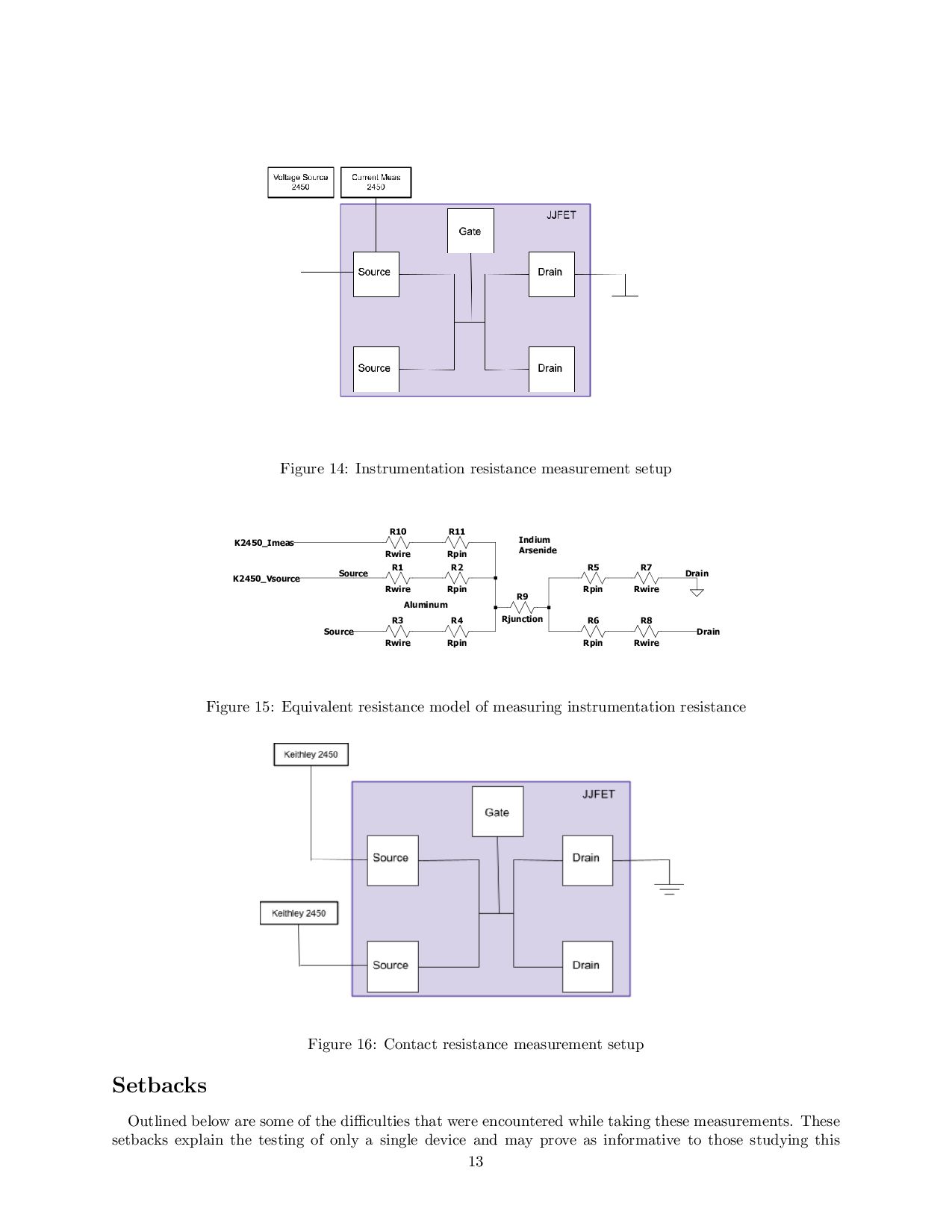
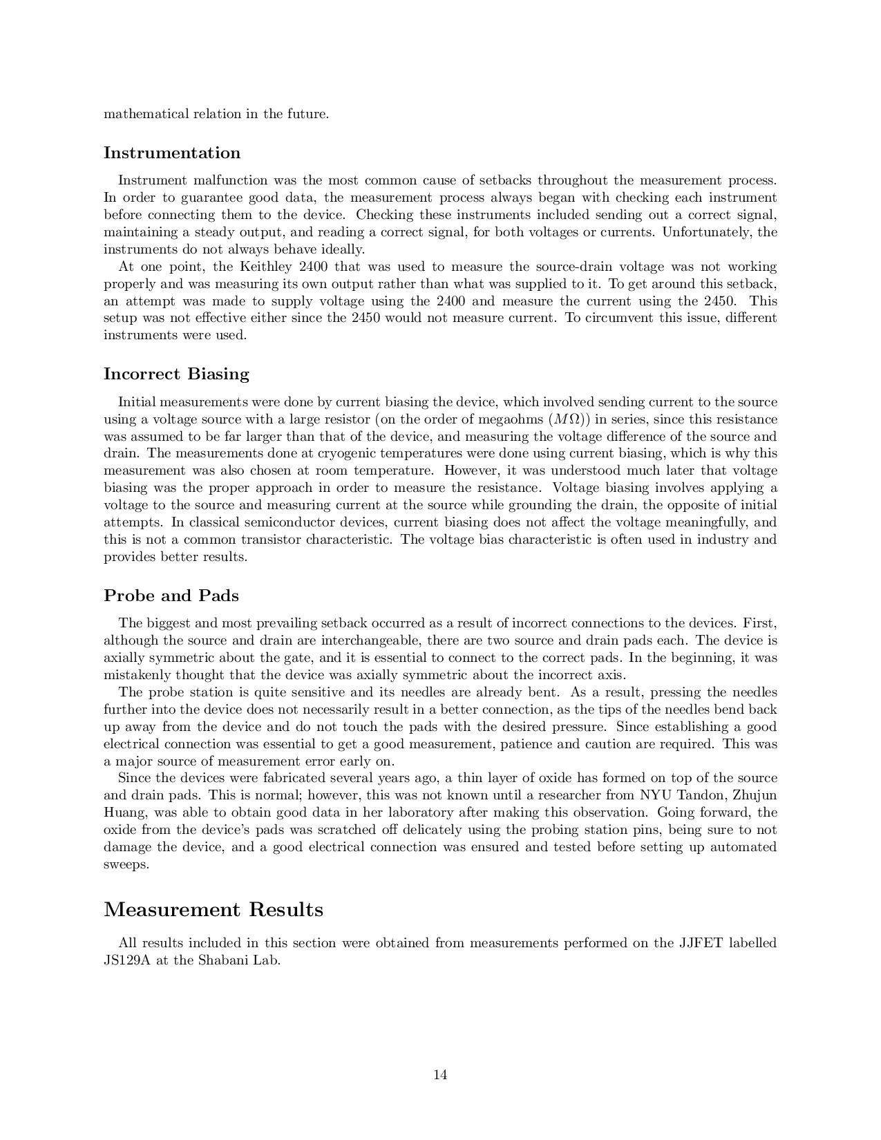
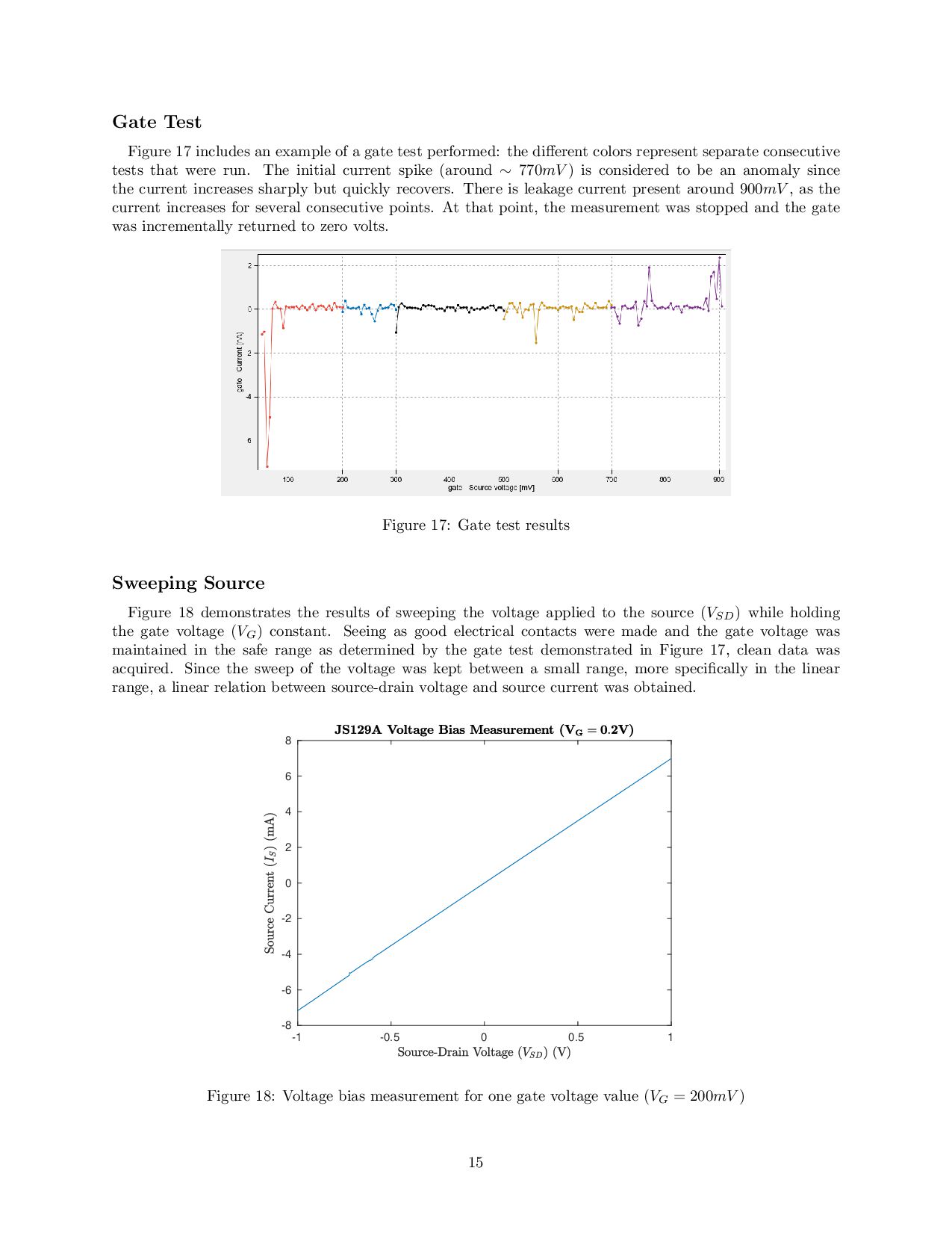
    . . . 54 ”Gate Voltage ( $V {G}$ ) (V) ” , . . . 55 ” D i f f e r e n t i a l Resistance ($R$) ( $\Omega$) ” , . . . 56 ” double sweep ” , lambda , ” a l l ”) ; 57 58 lambda = @(X, Y, Z) X ./ Z − median (Rc) ; 59 [ sweepGateSourceDevice , X, Y, Z ] = hdf5surf ( filename , 1 , 1 , 1 , 1 , . . . 60 ”\ bf JS129A Upper Bound Device Resistance ” , . . . 61 ”Source−Drain Voltage ( $V {SD}$ ) (V) ” , . . . 62 ”Gate Voltage ( $V {G}$ ) (V) ” , . . . 63 ” D i f f e r e n t i a l Resistance ($R$) ( $\Omega$) ” , . . . 64 ” d e v i c e r e s i s t a n c e ” , lambda , ” a l l ”) ; 65 66 67 h = f i g u r e ; 68 su rf (X( [ 1 : 6 , 8 : end ] , : ) , Y( [ 1 : 6 , 8 : end ] , : ) , Z ( [ 1 : 6 , 8 : end ] , : ) ) ; 69 t i t l e (”\ bf JS129A Upper Bound Device Resistance ( Without $\ bf V {G}=0.1$V) \\” , . . . 70 ” I n t e r p r e t e r ” , ”LaTeX”) ; 71 xlim ( [ min(X, [ ] , ” a l l ”) max(X, [ ] , ” a l l ”) ] ) ; 72 xlabel (” Source−Drain Voltage ( $V {SD}$ ) (V) ” , ” I n t e r p r e t e r ” , ”LaTeX”) ; 73 ylabel (” Gate Voltage ( $V {G}$ ) (V) ” , ” I n t e r p r e t e r ” , ”LaTeX”) ; 74 75 shading interp ; 76 colormap hot ; 77 c = colorbar ; 78 c . Label . String = ” D i f f e r e n t i a l Resistance ($R$) ( $\Omega$) ”; 79 c . Label . I n t e r p r e t e r = ”LaTeX”; 80 c . Label . FontSize = 11; 81 view (2) ; 82 83 set (h , ” Units ” , ” Inches ”) ; 84 pos = get (h , ” Position ”) ; 85 set (h , ”PaperPositionMode ” , ”Auto” , ”PaperUnits ” , ” Inches ” , . . . 86 ” PaperSize ” , [ pos (3) , pos (4) ] ) ; 87 print (h , ” remove dirty resistance ” , ”−dpdf ” , ”−r300 ”) ; 88 89 90 Vg = unique (Y, ” sorted ”) ; 91 Rn = mean(Z , 2) ; 92 93 h = f i g u r e ; 94 plot (Vg, Rn, ”DisplayName ” , ” All $V {G}$ Values ”) ; 95 hold on ; 96 plot (Vg ( [ 1 : 6 , 8: end ] ) , Rn( [ 1 : 6 , 8: end ] ) , . . . 97 ”DisplayName ” , ”Without $V {G}=0.1$V”) ; 98 t i t l e (”\ bf JS129A Resistance with Respect to Gate Voltage ” , . . . 99 ” I n t e r p r e t e r ” , ”LaTeX”) ; 100 l = legend (” Location ” , ” northwest ”) ; 101 set ( l , ” I n t e r p r e t e r ” , ”LaTeX”) ; 102 xlim ( [ min(Y, [ ] , ” a l l ”) max(Y, [ ] , ” a l l ”) ] ) ; 103 xlabel (” Gate Voltage ( $V {G}$ ) (V) ” , ” I n t e r p r e t e r ” , ”LaTeX”) ; 104 ylabel (”Mean Resistance ($R$) ( $\Omega$) ” , ” I n t e r p r e t e r ” , ”LaTeX”) ; 105 33
  34. 106 set (h , ” Units ” , ” Inches

    ”) ; 107 pos = get (h , ” Position ”) ; 108 set (h , ”PaperPositionMode ” , ”Auto” , ”PaperUnits ” , ” Inches ” , . . . 109 ” PaperSize ” , [ pos (3) , pos (4) ] ) ; 110 print (h , ” vg vs rn ” , ”−dpdf ” , ”−r300 ”) ; 111 112 113 h = f i g u r e ; 114 vsd = sweepGateSource ( : , 1 , : ) ; 115 i s = sweepGateSource ( : , 3 , : ) ; 116 fo r vg = unique ( sweepGateSource ( : , 2 , : ) ) . ’ 117 plot ( vsd ( sweepGateSource ( : , 2 , : ) == vg ) , . . . 118 i s ( sweepGateSource ( : , 2 , : ) == vg ) ∗10ˆ3 , . . . 119 ”DisplayName ” , s p r i n t f (” $V {G}=%dmV$” , round ( vg ∗10ˆ3) ) ) ; 120 hold on ; 121 end 122 t i t l e (”\ bf JS129A Total Resistance IV Curves ” , ” I n t e r p r e t e r ” , ”LaTeX”) ; 123 l = legend (” Location ” , ” northwest ”) ; 124 set ( l , ” I n t e r p r e t e r ” , ”LaTeX”) ; 125 xlim ( [ min( sweepGateSource ( : , 1 , : ) , [ ] , ” a l l ”) . . . 126 max( sweepGateSource ( : , 1 , : ) , [ ] , ” a l l ”) ] ) ; 127 xlabel (” Source−Drain Voltage ( $V {SD}$ ) (V) ” , ” I n t e r p r e t e r ” , ”LaTeX”) ; 128 ylabel (” Source Current ( $I {S}$ ) (mA) ” , ” I n t e r p r e t e r ” , ”LaTeX”) ; 129 130 set (h , ” Units ” , ” Inches ”) ; 131 pos = get (h , ” Position ”) ; 132 set (h , ”PaperPositionMode ” , ”Auto” , ”PaperUnits ” , ” Inches ” , . . . 133 ” PaperSize ” , [ pos (3) , pos (4) ] ) ; 134 print (h , ” d e v i c e i v c u r v e s ” , ”−dpdf ” , ”−r300 ”) ; 135 136 137 %% Sweeping Gate and Source Voltage Crygenic Temperatures 138 filename = ”JS127A BM001 062 . hdf5 ”; 139 lambda = @(X, Y, Z) Z ; 140 [ cryogenicData , X, Y, Z ] = hdf5surf ( filename , 1 , 1e9 , 1 , 1 , . . . 141 ”\ bf JS127A Cryogenic Resistance ” , . . . 142 ” Source Current ( $I {S}$ ) ( $\mu$A) ” , . . . 143 ”Gate Voltage ( $V {G}$ ) (V) ” , . . . 144 ” D i f f e r e n t i a l Resistance ( $R {N}$ ) ( $\Omega$) ” , . . . 145 ” c r y o g e n i c r e s i s t a n c e 1 ” , lambda , [1 2 3 ] ) ; 34