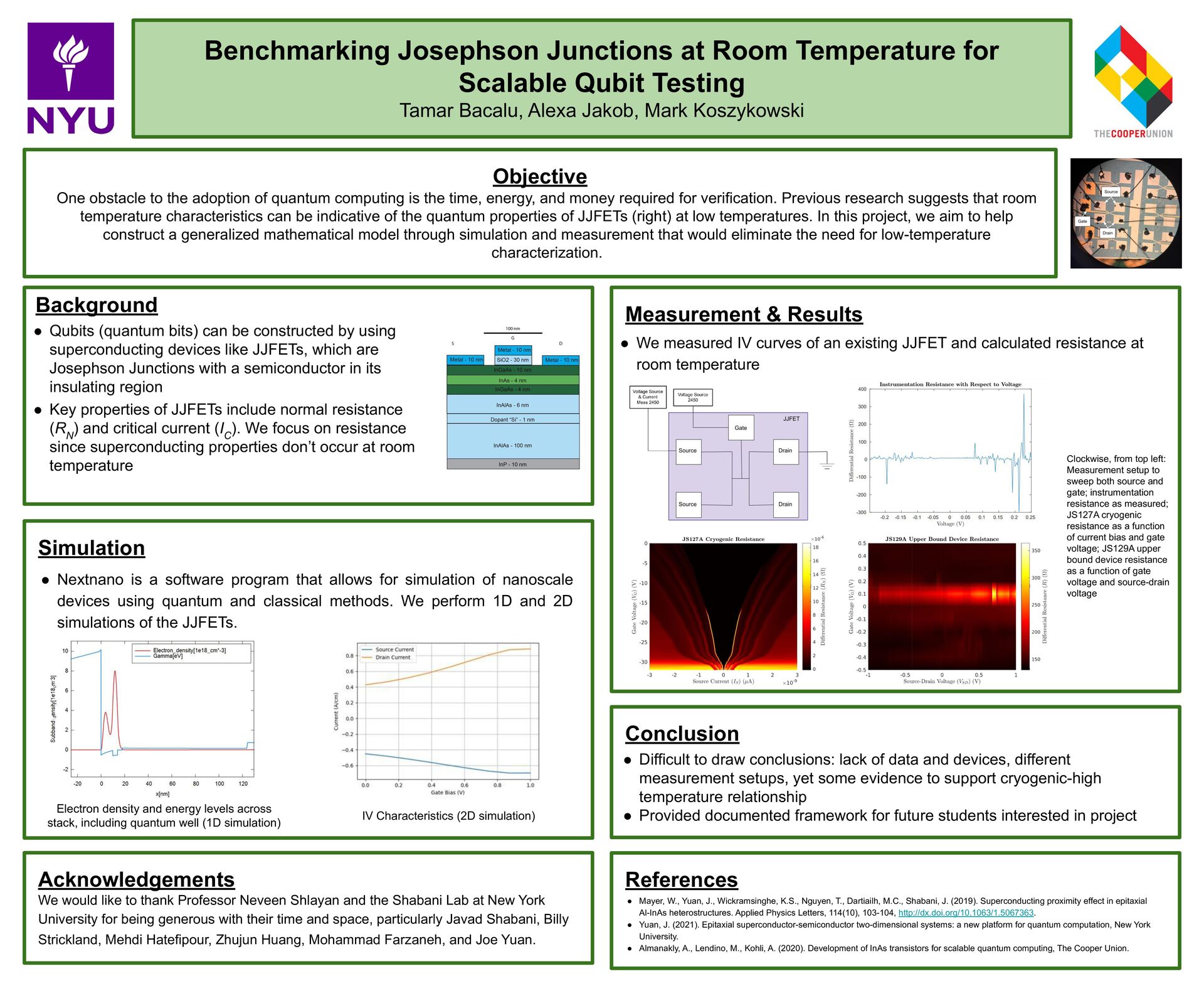
the time, energy, and money required for verification. Previous research suggests that room temperature characteristics can be indicative of the quantum properties of JJFETs (right) at low temperatures. In this project, we aim to help construct a generalized mathematical model through simulation and measurement that would eliminate the need for low-temperature characterization. References • Mayer, W., Yuan, J., Wickramsinghe, K.S., Nguyen, T., Dartiailh, M.C., Shabani, J. (2019). Superconducting proximity effect in epitaxial Al-InAs heterostructures. Applied Physics Letters, 114(10), 103-104, http://dx.doi.org/10.1063/1.5067363. • Yuan, J. (2021). Epitaxial superconductor-semiconductor two-dimensional systems: a new platform for quantum computation, New York University. • Almanakly, A., Lendino, M., Kohli, A. (2020). Development of InAs transistors for scalable quantum computing, The Cooper Union. Benchmarking Josephson Junctions at Room Temperature for Scalable Qubit Testing Tamar Bacalu, Alexa Jakob, Mark Koszykowski Simulation Measurement & Results Background • Qubits (quantum bits) can be constructed by using superconducting devices like JJFETs, which are Josephson Junctions with a semiconductor in its insulating region • Key properties of JJFETs include normal resistance (R N ) and critical current (I C ). We focus on resistance since superconducting properties don’t occur at room temperature Electron density and energy levels across stack, including quantum well (1D simulation) IV Characteristics (2D simulation) • We measured IV curves of an existing JJFET and calculated resistance at room temperature • Nextnano is a software program that allows for simulation of nanoscale devices using quantum and classical methods. We perform 1D and 2D simulations of the JJFETs. Acknowledgements We would like to thank Professor Neveen Shlayan and the Shabani Lab at New York University for being generous with their time and space, particularly Javad Shabani, Billy Strickland, Mehdi Hatefipour, Zhujun Huang, Mohammad Farzaneh, and Joe Yuan. Clockwise, from top left: Measurement setup to sweep both source and gate; instrumentation resistance as measured; JS127A cryogenic resistance as a function of current bias and gate voltage; JS129A upper bound device resistance as a function of gate voltage and source-drain voltage Conclusion • Difficult to draw conclusions: lack of data and devices, different measurement setups, yet some evidence to support cryogenic-high temperature relationship • Provided documented framework for future students interested in project