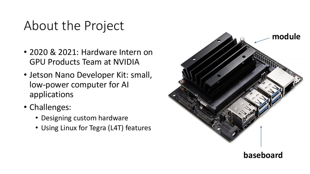
GPU Products Team at NVIDIA • Jetson Nano Developer Kit: small, low-power computer for AI applications • Challenges: • Designing custom hardware • Using Linux for Tegra (L4T) features module baseboard
talk to engineers • Main concerns: • Difficult to find simple hardware projects • No example boards for hardware design • Open source files are inaccessible
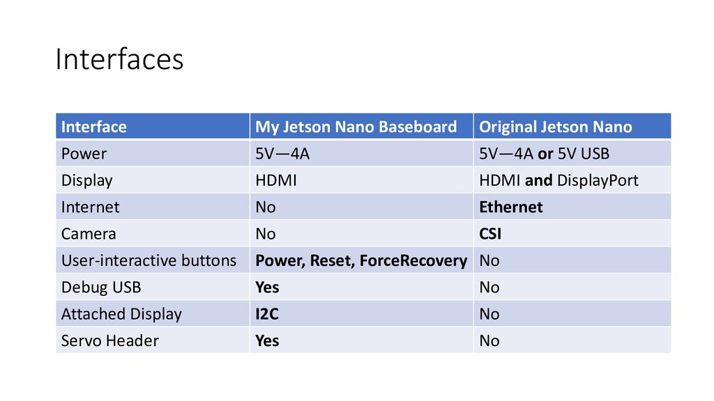
5V—4A 5V—4A or 5V USB Display HDMI HDMI and DisplayPort Internet No Ethernet Camera No CSI User-interactive buttons Power, Reset, ForceRecovery No Debug USB Yes No Attached Display I2C No Servo Header Yes No
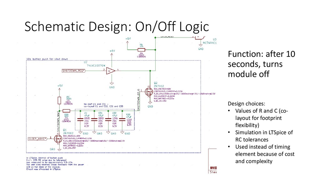
off Design choices: • Values of R and C (co- layout for footprint flexibility) • Simulation in LTSpice of RC tolerances • Used instead of timing element because of cost and complexity
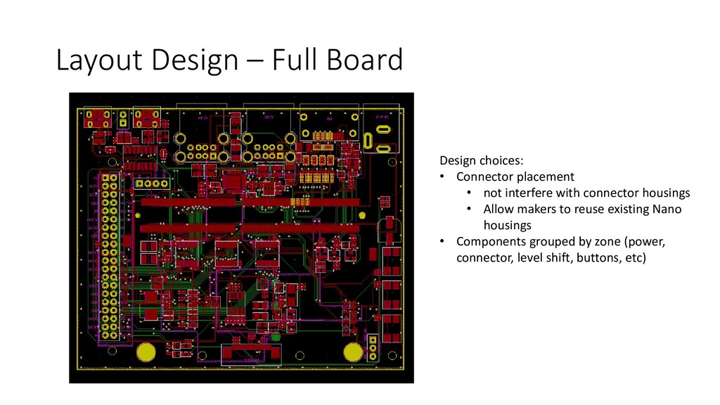
• not interfere with connector housings • Allow makers to reuse existing Nano housings • Components grouped by zone (power, connector, level shift, buttons, etc)
JLCPCB chosen: inexpensive, quick turnaround • Parts in library vs parts bought separately: NVIDIA technicians did some soldering • Final cost: $440/10 boards (vs $99 for 1 dev kit) • PCB assembly, parts, stencils, shipping
diode/transistor characteristics • Functional: testing all interfaces for functionality • Electrical: IO meets specifications • Power: test efficiency, noise, characteristics of power sources & test power sequencing * Electrical and power validation not performed due to time and equipment constraints working from home
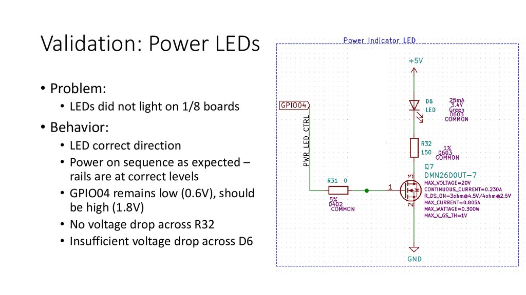
on 1/8 boards • Behavior: • LED correct direction • Power on sequence as expected – rails are at correct levels • GPIO04 remains low (0.6V), should be high (1.8V) • No voltage drop across R32 • Insufficient voltage drop across D6
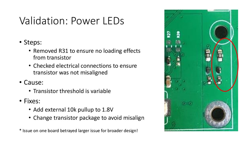
no loading effects from transistor • Checked electrical connections to ensure transistor was not misaligned • Cause: • Transistor threshold is variable • Fixes: • Add external 10k pullup to 1.8V • Change transistor package to avoid misalign * Issue on one board betrayed larger issue for broader design!
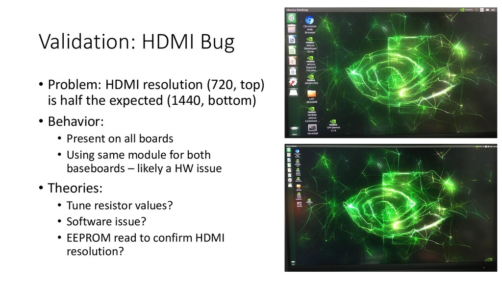
half the expected (1440, bottom) • Behavior: • Present on all boards • Using same module for both baseboards – likely a HW issue • Theories: • Tune resistor values? • Software issue? • EEPROM read to confirm HDMI resolution?
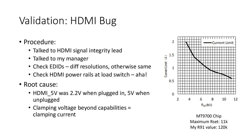
integrity lead • Talked to my manager • Check EDIDs – diff resolutions, otherwise same • Check HDMI power rails at load switch – aha! • Root cause: • HDMI_5V was 2.2V when plugged in, 5V when unplugged • Clamping voltage beyond capabilities = clamping current MT9700 Chip Maximum Rset: 11k My R91 value: 120k
• Advice from Design, Layout, Software Engineers • Legal • Developed appropriate license for open-source project • Marketing & Developer Relations • Filmed series of videos for Instagram and YouTube • Advised sample projects • Signal Integrity • Advised differential pair design and layout
educational videos about the design process • Videos for TikTok & YouTube on the NVIDIA Embedded channel • Participated in intern panel talking about project