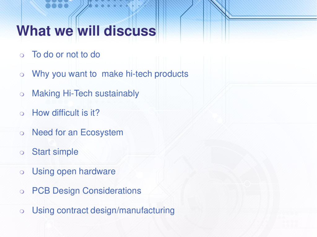
do Why you want to make hi-tech products Making Hi-Tech sustainably How difficult is it? Need for an Ecosystem Start simple Using open hardware PCB Design Considerations Using contract design/manufacturing
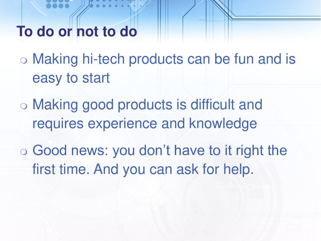
can be fun and is easy to start Making good products is difficult and requires experience and knowledge Good news: you don’t have to it right the first time. And you can ask for help.
job creation. Hi-tech manufacturing creates one of the highest rate of low-skilled jobs Locality: local manufacturing gives the home company an unbeatable advantage over companies that have to ship-in their products from abroad. A service built behind a hardware product locks- in customers and therefore guarantees a continuous income stream.
you higher than your cost of production, which usually includes cost of replacing devices that go bad during warranty. Long-term sustainability requires that our products be globally competitive. Foreign companies with better technology and more money are the ultimate competition. This is the tough part!
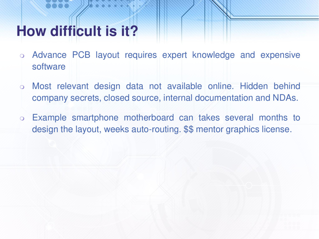
knowledge and expensive software Most relevant design data not available online. Hidden behind company secrets, closed source, internal documentation and NDAs. Example smartphone motherboard can takes several months to design the layout, weeks auto-routing. $$ mentor graphics license.
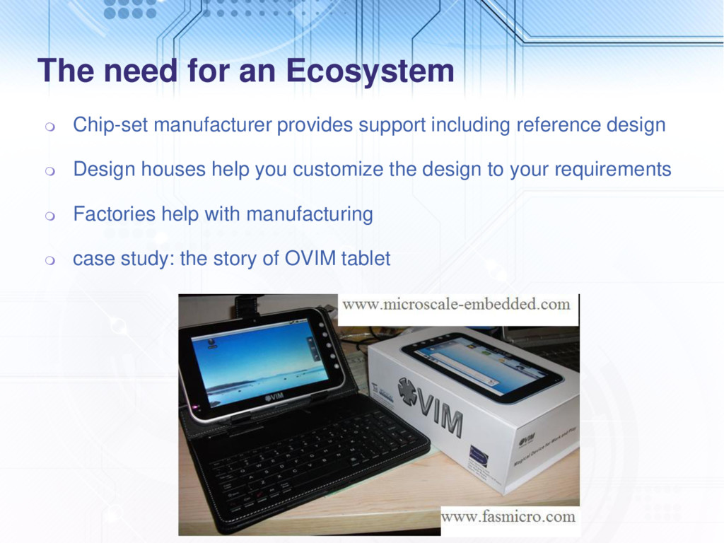
including reference design Design houses help you customize the design to your requirements Factories help with manufacturing case study: the story of OVIM tablet
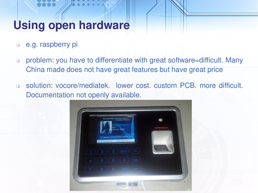
have to differentiate with great software=difficult. Many China made does not have great features but have great price solution: vocore/mediatek. lower cost. custom PCB. more difficult. Documentation not openly available.
schematic that has been validated by simulation does not mean the PCB will work automatically. High-speed PCB design described as black-magic Problems include EMC, cross-talk, trace inductance/capacitance, component placements, skew etc.
schematic capture program allows the user to draw a document representing the electrical component symbols and the interconnections between them in a graphical way. Before generating a PCB, the symbols are mapped to component footprints and the symbol interconnections are converted to a netlist that specifies the connections between the component footprints in the layout process. A schematic tool that allows the user to do interactive circuit simulation with the same schematic circuit representation used for layout is advantageous. Circuit simulation can be useful for both initial design analysis and testing the design (i.e. verification testing and troubleshooting) once complete.
PCB layout program generates the mechanical and wiring connection structure of the PCB from the netlist. The layout program allows the wiring connection structure to be placed on multiple layers and, once complete, allows the user to generate the computer aided design (CAD) files needed to manufacture a PCB. Gerber files – The CAD files that need to be sent to a PCB manufacturer so it can build the PCB layer structure are called Gerber files. The RS-274X is the most commonly supported Gerber file format. NC drill files – The numerically controlled (NC) drill files indicate the size and position of holes used for unplated holes, plated through- holes, or holes for vias. Some quick-turn PCB manufacturers have only select hole sizes available.
a PCB, typically comprised of fiberglass, which provides the rigidity and thickness to a PCB Copper – A thin copper foil layer is laminated to the board with heat and adhesive. For double-sided PCBs, the copper layer is laminated to both sides of the board. Soldermask – The soldermask layer is found on top of the copper layer and gives the PCB its color — often, the traditional green, although it may also be another color. The soldermask is designed to insulate the copper from other metals, solder, or other conductive bits to prevent unintentional contact. It also aids the user in soldering in the correct locations, preventing solder jumpers. Silkscreen – The silkscreen layer is applied on top of the soldermask layer and adds markings (numbers, letters, and symbols) to guide assembly and aid in understanding the board. Silkscreen layers can be used to label the functions of pins, LEDs, and other components, and while they’re typically white, other colors (black, grey, red, etc.) are possible. It’s uncommon to use more than one silkscreen color on a single board.
direction to reduce the likelihood of soldering errors. On the solder side of the board, don’t place components opposite plated through-hole components on the other side of the board. As a general rule, keep SMT (Surface Mount) components on the same side of the board. Likewise, keep all through-hole components on the top side of the board. Doing so reduces the number of assembly steps.
and placed on the interior area of the board. Avoid creating chains of power lines from part to part. If you have sensitive signals, you’ll want to ensure that those signals are adequately shielded from noise sources using planes. For any components that absorb 10 mW or greater, as well as components that conduct 10 mA or more, you should carefully weigh thermal and electrical considerations.
either ground planes or power planes for heat flow. For high-current connections, follow the accepted voltage drop for the connection. There should be two to four vias for at each layer transition for high- current paths. Additionally, having multiple vias at each layer transition offers benefits such as improved reliability and thermal conductivity, as well as reduced inductive and resistive losses. Signal traces should be placed according to your schematic guideline and should be as short and direct as possible between components.
damage a PCB. Consult the thermal resistance ratings for each component, and determine which components dissipate the most heat. Make sure that critical components are placed at an ample distance from high-heat components. Always use thermal reliefs on through-hole components, and use a thermal relief pattern for all vias and holes connected to ground or power planes. Teardrops can also be used for added copper/metal support and to reduce mechanical and thermal stress.