Upgrade to Pro — share decks privately, control downloads, hide ads and more …

Nanonics Imaging Ltd.

Nanonics Imaging Ltd.

Nanonics produces AFM/SPM systems with unique design for overcoming limitations of standard SPM system. Nanonics offers unique capabilities for integrated microscope of combining SPM with optical microscopy, analytical devices (e.g. Raman) and multiprobe operation.

Avatar for Nanonics Imaging Ltd.

Nanonics Imaging Ltd.

March 25, 2015

Other Decks in Technology

Transcript

  1. The Next Evolution In AFM Nanonics produces AFM/SPM systems with

    unique design for overcoming limitations of standard SPM system. Nanonics offers unique capabilities for integrated microscope of combining SPM with optical microscopy, analytical devices (e.g. Raman) and multiprobe operation. Nanonics opened the door and pioneered many new fields in SPM that became a standard in this market. The following are examples: • MultiProbe SPM systems • AFM/Raman and TERS • Near-field Scanning Optical Microscopy (NSOM and sSNOM) • Ultimate BioAFM Hydra with Tuning Fork feedback • Fountain Pen Nanolithography • SPM/FIB/SEM Integra ration
  2. The Next Evolution In AFM Nanonics covers a wide range

    of the Nanoscience and Nanotechnology spectrum: • SPM various modes • Online AFM/Raman • TERS • Near-field and Far-field microscopy combined with SPM (NSOM and Apertureless) • Photonics • Plasmonics • BioSPM • Nanolithography • Multiprobe imaging and nanomanipulation, • Nano-Electrical/Thermal, • Low temperature SPM and integration with FIB/SEM. Visit our website for more information or to get a quote: www.nanonics.co.il
  3. The Next Evolution In AFM MultiView 1000TM MultiView 2000TM MultiView

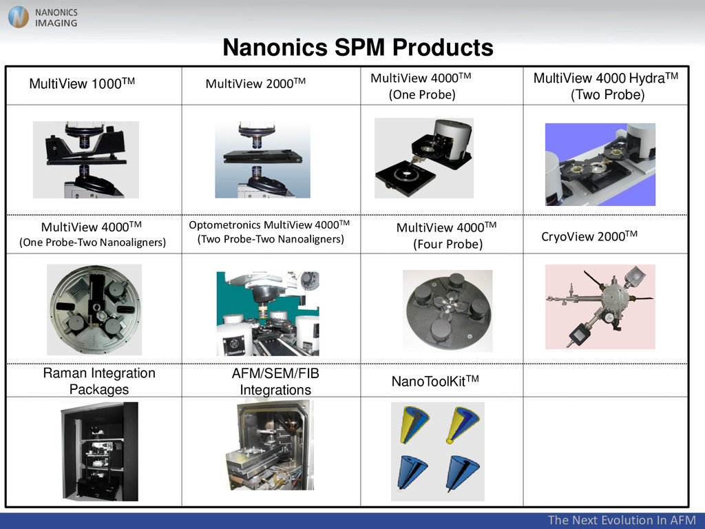
    4000TM (One Probe) MultiView 4000 HydraTM (Two Probe) MultiView 4000TM (One Probe-Two Nanoaligners) Optometronics MultiView 4000TM (Two Probe-Two Nanoaligners) MultiView 4000TM (Four Probe) CryoView 2000TM Raman Integration Packages AFM/SEM/FIB Integrations NanoToolKitTM Nanonics SPM Products
  4. The Next Evolution In AFM Unique SPM Design for Free

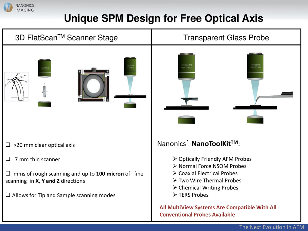
    Optical Axis 3D FlatScanTM Scanner Stage Transparent Glass Probe  >20 mm clear optical axis  7 mm thin scanner  mms of rough scanning and up to 100 micron of fine scanning in X, Y and Z directions  Allows for Tip and Sample scanning modes Nanonics’ NanoToolKitTM:  Optically Friendly AFM Probes  Normal Force NSOM Probes  Coaxial Electrical Probes  Two Wire Thermal Probes  Chemical Writing Probes  TERS Probes All MultiView Systems Are Compatible With All Conventional Probes Available
  5. The Next Evolution In AFM NSOM/SNOM Near Field Scanning Optical

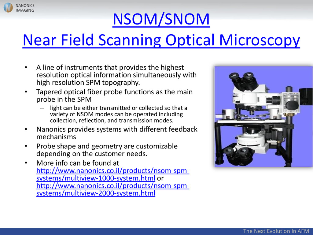
    Microscopy • A line of instruments that provides the highest resolution optical information simultaneously with high resolution SPM topography. • Tapered optical fiber probe functions as the main probe in the SPM – light can be either transmitted or collected so that a variety of NSOM modes can be operated including collection, reflection, and transmission modes. • Nanonics provides systems with different feedback mechanisms • Probe shape and geometry are customizable depending on the customer needs. • More info can be found at http://www.nanonics.co.il/products/nsom-spm- systems/multiview-1000-system.html or http://www.nanonics.co.il/products/nsom-spm- systems/multiview-2000-system.html
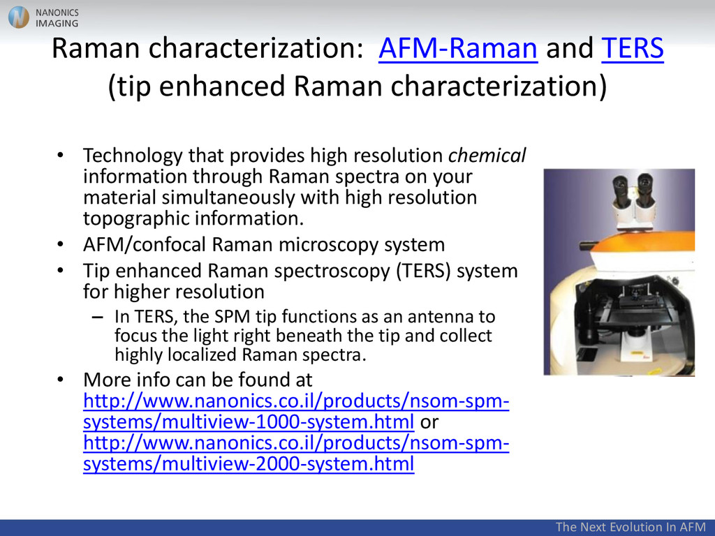
  6. The Next Evolution In AFM Raman characterization: AFM-Raman and TERS

    (tip enhanced Raman characterization) • Technology that provides high resolution chemical information through Raman spectra on your material simultaneously with high resolution topographic information. • AFM/confocal Raman microscopy system • Tip enhanced Raman spectroscopy (TERS) system for higher resolution – In TERS, the SPM tip functions as an antenna to focus the light right beneath the tip and collect highly localized Raman spectra. • More info can be found at http://www.nanonics.co.il/products/nsom-spm- systems/multiview-1000-system.html or http://www.nanonics.co.il/products/nsom-spm- systems/multiview-2000-system.html
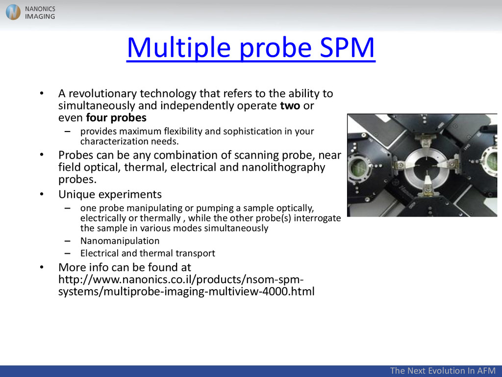
  7. The Next Evolution In AFM Multiple probe SPM • A

    revolutionary technology that refers to the ability to simultaneously and independently operate two or even four probes – provides maximum flexibility and sophistication in your characterization needs. • Probes can be any combination of scanning probe, near field optical, thermal, electrical and nanolithography probes. • Unique experiments – one probe manipulating or pumping a sample optically, electrically or thermally , while the other probe(s) interrogate the sample in various modes simultaneously – Nanomanipulation – Electrical and thermal transport • More info can be found at http://www.nanonics.co.il/products/nsom-spm- systems/multiprobe-imaging-multiview-4000.html
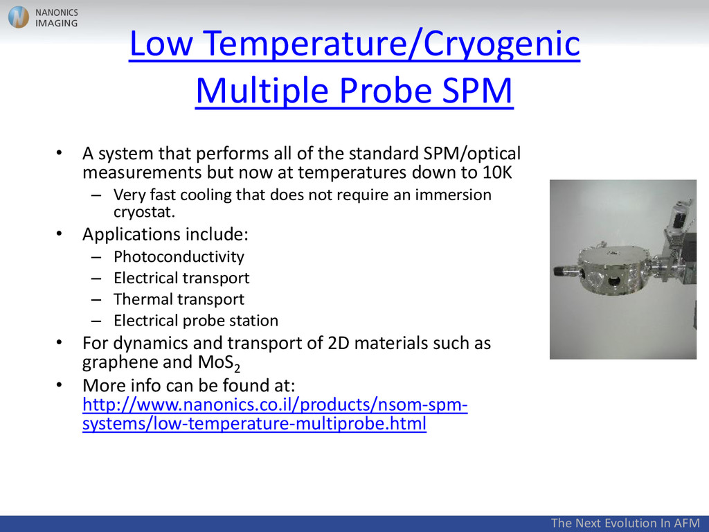
  8. The Next Evolution In AFM Low Temperature/Cryogenic Multiple Probe SPM

    • A system that performs all of the standard SPM/optical measurements but now at temperatures down to 10K – Very fast cooling that does not require an immersion cryostat. • Applications include: – Photoconductivity – Electrical transport – Thermal transport – Electrical probe station • For dynamics and transport of 2D materials such as graphene and MoS2 • More info can be found at: http://www.nanonics.co.il/products/nsom-spm- systems/low-temperature-multiprobe.html
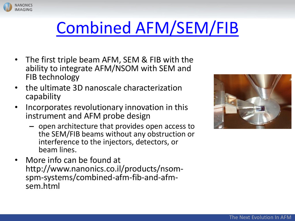
  9. The Next Evolution In AFM Combined AFM/SEM/FIB • The first

    triple beam AFM, SEM & FIB with the ability to integrate AFM/NSOM with SEM and FIB technology • the ultimate 3D nanoscale characterization capability • Incorporates revolutionary innovation in this instrument and AFM probe design – open architecture that provides open access to the SEM/FIB beams without any obstruction or interference to the injectors, detectors, or beam lines. • More info can be found at http://www.nanonics.co.il/products/nsom- spm-systems/combined-afm-fib-and-afm- sem.html