A Modern DSP Based Lock-In Amplifier Designed for Code and Hardware Experimentation
Describes a open hardware / software instrument that is used to make very low level measurements. The open nature of the design allows for fast experimentation with new algorithms very easy.
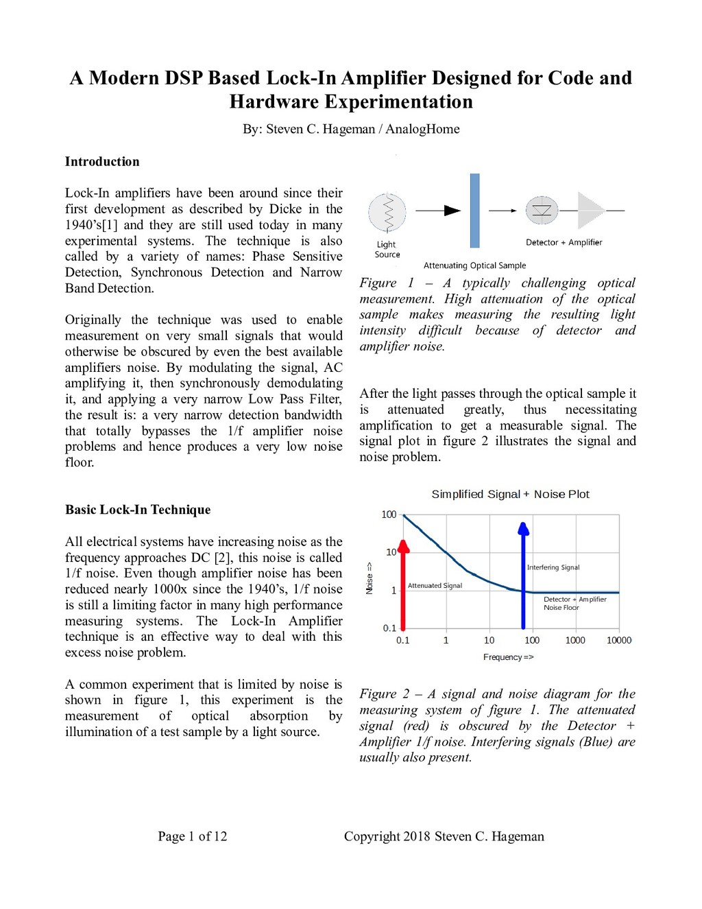
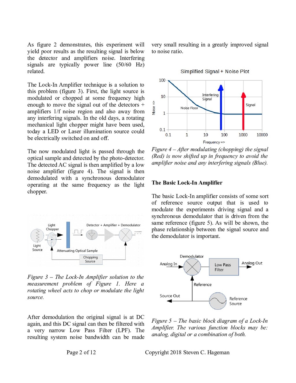
Hardware Experimentation By: Steven C. Hageman / AnalogHome Introduction Lock-In amplifiers have been around since their first development as described by Dicke in the 1940’s[1] and they are still used today in many experimental systems. The technique is also called by a variety of names: Phase Sensitive Detection, Synchronous Detection and Narrow Band Detection. Originally the technique was used to enable measurement on very small signals that would otherwise be obscured by even the best available amplifiers noise. By modulating the signal, AC amplifying it, then synchronously demodulating it, and applying a very narrow Low Pass Filter, the result is: a very narrow detection bandwidth that totally bypasses the 1/f amplifier noise problems and hence produces a very low noise floor. Basic Lock-In Technique All electrical systems have increasing noise as the frequency approaches DC [2], this noise is called 1/f noise. Even though amplifier noise has been reduced nearly 1000x since the 1940’s, 1/f noise is still a limiting factor in many high performance measuring systems. The Lock-In Amplifier technique is an effective way to deal with this excess noise problem. A common experiment that is limited by noise is shown in figure 1, this experiment is the measurement of optical absorption by illumination of a test sample by a light source. Figure 1 – A typically challenging optical measurement. High attenuation of the optical sample makes measuring the resulting light intensity difficult because of detector and amplifier noise. After the light passes through the optical sample it is attenuated greatly, thus necessitating amplification to get a measurable signal. The signal plot in figure 2 illustrates the signal and noise problem. Figure 2 – A signal and noise diagram for the measuring system of figure 1. The attenuated signal (red) is obscured by the Detector + Amplifier 1/f noise. Interfering signals (Blue) are usually also present. Page 1 of 12 Copyright 2018 Steven C. Hageman
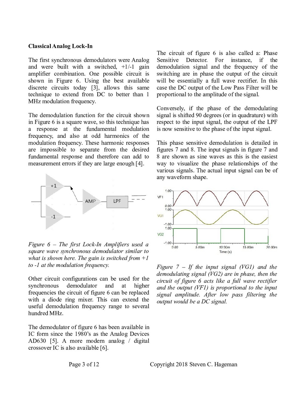
as the resulting signal is below the detector and amplifiers noise. Interfering signals are typically power line (50/60 Hz) related. The Lock-In Amplifier technique is a solution to this problem (figure 3). First, the light source is modulated or chopped at some frequency high enough to move the signal out of the detectors + amplifiers 1/f noise region and also away from any interfering signals. In the old days, a rotating mechanical light chopper might have been used, today a LED or Laser illumination source could be electrically switched on and off. The now modulated light is passed through the optical sample and detected by the photo-detector. The detected AC signal is then amplified by a low noise amplifier (figure 4). The signal is then demodulated with a synchronous demodulator operating at the same frequency as the light chopper. Figure 3 – The Lock-In Amplifier solution to the measurement problem of Figure 1. Here a rotating wheel acts to chop or modulate the light source. After demodulation the original signal is at DC again, and this DC signal can then be filtered with a very narrow Low Pass Filter (LPF). The resulting system noise bandwidth can be made very small resulting in a greatly improved signal to noise ratio. Figure 4 – After modulating (chopping) the signal (Red) is now shifted up in frequency to avoid the amplifier noise and any interfering signals (Blue). The Basic Lock-In Amplifier The basic Lock-In amplifier consists of some sort of reference source output that is used to modulate the experiments driving signal and a synchronous demodulator that is driven from the same reference (figure 5). As will be shown, the phase relationship between the signal source and the demodulator is important. Figure 5 – The basic block diagram of a Lock-In Amplifier. The various function blocks may be: analog, digital or a combination of both. Page 2 of 12 Copyright 2018 Steven C. Hageman
were built with a switched, +1/-1 gain amplifier combination. One possible circuit is shown in Figure 6. Using the best available discrete circuits today [3], allows this same technique to extend from DC to better than 1 MHz modulation frequency. The demodulation function for the circuit shown in Figure 6 is a square wave, so this technique has a response at the fundamental modulation frequency, and also at odd harmonics of the modulation frequency. These harmonic responses are impossible to separate from the desired fundamental response and therefore can add to measurement errors if they are large enough [4]. Figure 6 – The first Lock-In Amplifiers used a square wave synchronous demodulator similar to what is shown here. The gain is switched from +1 to -1 at the modulation frequency. Other circuit configurations can be used for the synchronous demodulator and at higher frequencies the circuit of figure 6 can be replaced with a diode ring mixer. This can extend the useful demodulation frequency range to several hundred MHz. The demodulator of figure 6 has been available in IC form since the 1980’s as the Analog Devices AD630 [5]. A more modern analog / digital crossover IC is also available [6]. The circuit of figure 6 is also called a: Phase Sensitive Detector. For instance, if the demodulation signal and the frequency of the switching are in phase the output of the circuit will be essentially a full wave rectifier. In this case the DC output of the Low Pass Filter will be proportional to the amplitude of the signal. Conversely, if the phase of the demodulating signal is shifted 90 degrees (or in quadrature) with respect to the input signal, the output of the LPF is now sensitive to the phase of the input signal. This phase sensitive demodulation is detailed in figures 7 and 8. The input signals in figure 7 and 8 are shown as sine waves as this is the easiest way to visualize the phase relationships of the various signals. The actual input signal can be of any waveform shape. Figure 7 – If the input signal (VG1) and the demodulating signal (VG2) are in phase, then the circuit of figure 6 acts like a full wave rectifier and the output (VF1) is proportional to the input signal amplitude. After low pass filtering the output would be a DC signal. Page 3 of 12 Copyright 2018 Steven C. Hageman
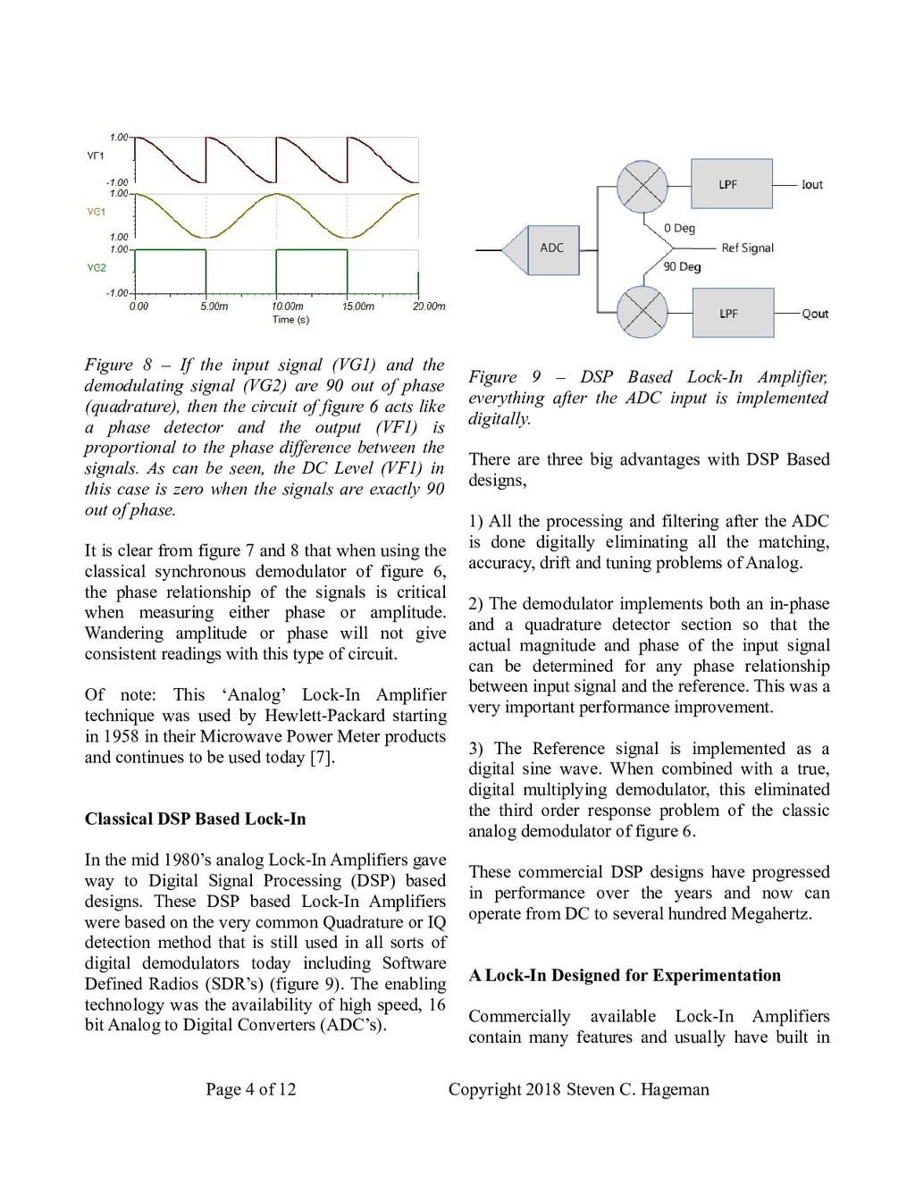
demodulating signal (VG2) are 90 out of phase (quadrature), then the circuit of figure 6 acts like a phase detector and the output (VF1) is proportional to the phase difference between the signals. As can be seen, the DC Level (VF1) in this case is zero when the signals are exactly 90 out of phase. It is clear from figure 7 and 8 that when using the classical synchronous demodulator of figure 6, the phase relationship of the signals is critical when measuring either phase or amplitude. Wandering amplitude or phase will not give consistent readings with this type of circuit. Of note: This ‘Analog’ Lock-In Amplifier technique was used by Hewlett-Packard starting in 1958 in their Microwave Power Meter products and continues to be used today [7]. Classical DSP Based Lock-In In the mid 1980’s analog Lock-In Amplifiers gave way to Digital Signal Processing (DSP) based designs. These DSP based Lock-In Amplifiers were based on the very common Quadrature or IQ detection method that is still used in all sorts of digital demodulators today including Software Defined Radios (SDR’s) (figure 9). The enabling technology was the availability of high speed, 16 bit Analog to Digital Converters (ADC’s). Figure 9 – DSP Based Lock-In Amplifier, everything after the ADC input is implemented digitally. There are three big advantages with DSP Based designs, 1) All the processing and filtering after the ADC is done digitally eliminating all the matching, accuracy, drift and tuning problems of Analog. 2) The demodulator implements both an in-phase and a quadrature detector section so that the actual magnitude and phase of the input signal can be determined for any phase relationship between input signal and the reference. This was a very important performance improvement. 3) The Reference signal is implemented as a digital sine wave. When combined with a true, digital multiplying demodulator, this eliminated the third order response problem of the classic analog demodulator of figure 6. These commercial DSP designs have progressed in performance over the years and now can operate from DC to several hundred Megahertz. A Lock-In Designed for Experimentation Commercially available Lock-In Amplifiers contain many features and usually have built in Page 4 of 12 Copyright 2018 Steven C. Hageman
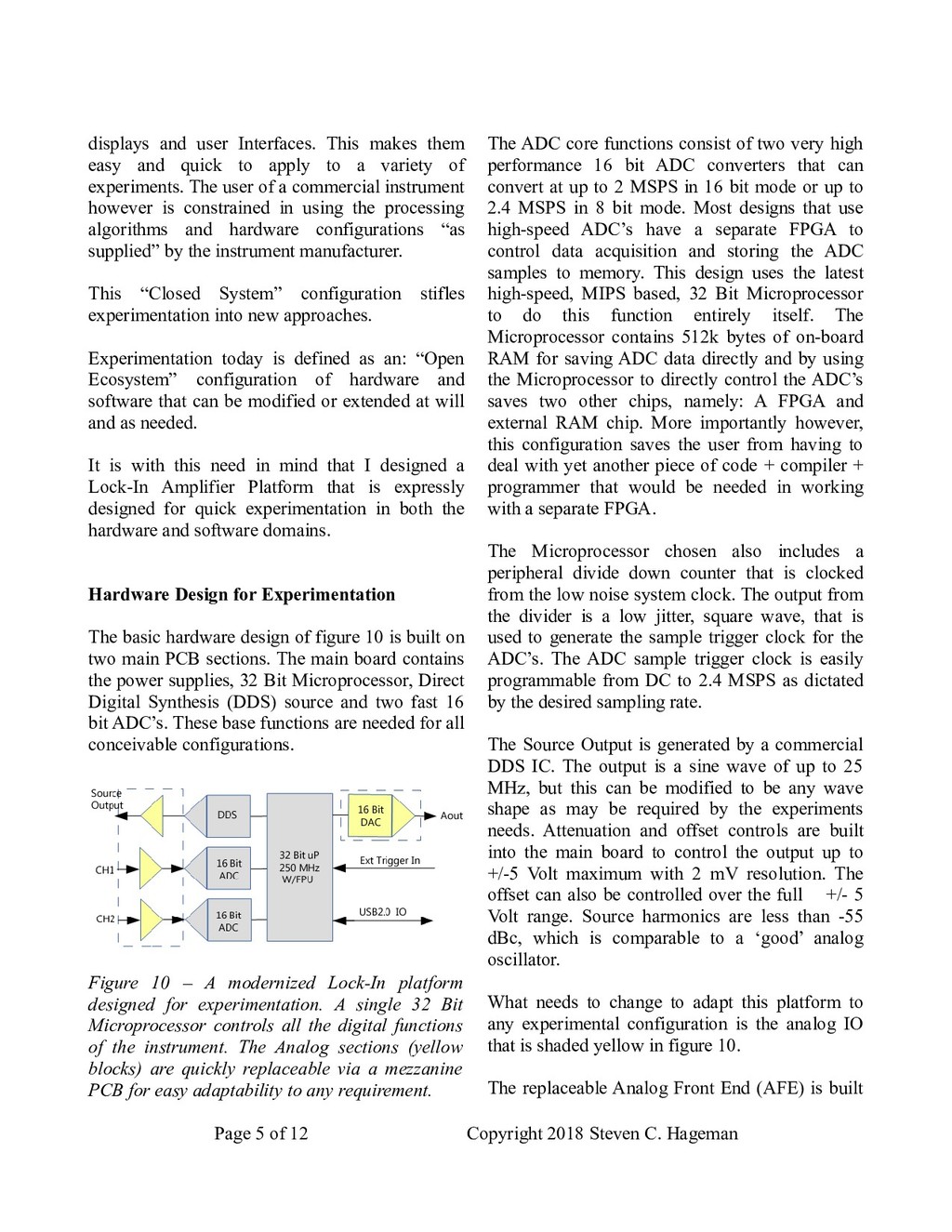
to apply to a variety of experiments. The user of a commercial instrument however is constrained in using the processing algorithms and hardware configurations “as supplied” by the instrument manufacturer. This “Closed System” configuration stifles experimentation into new approaches. Experimentation today is defined as an: “Open Ecosystem” configuration of hardware and software that can be modified or extended at will and as needed. It is with this need in mind that I designed a Lock-In Amplifier Platform that is expressly designed for quick experimentation in both the hardware and software domains. Hardware Design for Experimentation The basic hardware design of figure 10 is built on two main PCB sections. The main board contains the power supplies, 32 Bit Microprocessor, Direct Digital Synthesis (DDS) source and two fast 16 bit ADC’s. These base functions are needed for all conceivable configurations. Figure 10 – A modernized Lock-In platform designed for experimentation. A single 32 Bit Microprocessor controls all the digital functions of the instrument. The Analog sections (yellow blocks) are quickly replaceable via a mezzanine PCB for easy adaptability to any requirement. The ADC core functions consist of two very high performance 16 bit ADC converters that can convert at up to 2 MSPS in 16 bit mode or up to 2.4 MSPS in 8 bit mode. Most designs that use high-speed ADC’s have a separate FPGA to control data acquisition and storing the ADC samples to memory. This design uses the latest high-speed, MIPS based, 32 Bit Microprocessor to do this function entirely itself. The Microprocessor contains 512k bytes of on-board RAM for saving ADC data directly and by using the Microprocessor to directly control the ADC’s saves two other chips, namely: A FPGA and external RAM chip. More importantly however, this configuration saves the user from having to deal with yet another piece of code + compiler + programmer that would be needed in working with a separate FPGA. The Microprocessor chosen also includes a peripheral divide down counter that is clocked from the low noise system clock. The output from the divider is a low jitter, square wave, that is used to generate the sample trigger clock for the ADC’s. The ADC sample trigger clock is easily programmable from DC to 2.4 MSPS as dictated by the desired sampling rate. The Source Output is generated by a commercial DDS IC. The output is a sine wave of up to 25 MHz, but this can be modified to be any wave shape as may be required by the experiments needs. Attenuation and offset controls are built into the main board to control the output up to +/-5 Volt maximum with 2 mV resolution. The offset can also be controlled over the full +/- 5 Volt range. Source harmonics are less than -55 dBc, which is comparable to a ‘good’ analog oscillator. What needs to change to adapt this platform to any experimental configuration is the analog IO that is shaded yellow in figure 10. The replaceable Analog Front End (AFE) is built Page 5 of 12 Copyright 2018 Steven C. Hageman
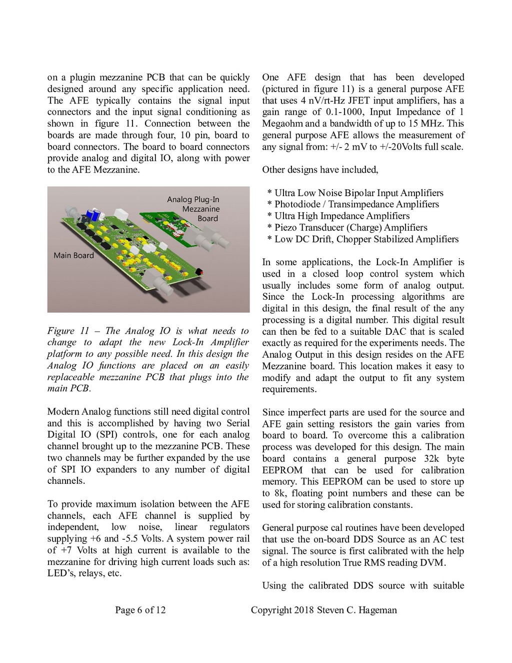
around any specific application need. The AFE typically contains the signal input connectors and the input signal conditioning as shown in figure 11. Connection between the boards are made through four, 10 pin, board to board connectors. The board to board connectors provide analog and digital IO, along with power to the AFE Mezzanine. Figure 11 – The Analog IO is what needs to change to adapt the new Lock-In Amplifier platform to any possible need. In this design the Analog IO functions are placed on an easily replaceable mezzanine PCB that plugs into the main PCB. Modern Analog functions still need digital control and this is accomplished by having two Serial Digital IO (SPI) controls, one for each analog channel brought up to the mezzanine PCB. These two channels may be further expanded by the use of SPI IO expanders to any number of digital channels. To provide maximum isolation between the AFE channels, each AFE channel is supplied by independent, low noise, linear regulators supplying +6 and -5.5 Volts. A system power rail of +7 Volts at high current is available to the mezzanine for driving high current loads such as: LED’s, relays, etc. One AFE design that has been developed (pictured in figure 11) is a general purpose AFE that uses 4 nV/rt-Hz JFET input amplifiers, has a gain range of 0.1-1000, Input Impedance of 1 Megaohm and a bandwidth of up to 15 MHz. This general purpose AFE allows the measurement of any signal from: +/- 2 mV to +/-20Volts full scale. Other designs have included, * Ultra Low Noise Bipolar Input Amplifiers * Photodiode / Transimpedance Amplifiers * Ultra High Impedance Amplifiers * Piezo Transducer (Charge) Amplifiers * Low DC Drift, Chopper Stabilized Amplifiers In some applications, the Lock-In Amplifier is used in a closed loop control system which usually includes some form of analog output. Since the Lock-In processing algorithms are digital in this design, the final result of the any processing is a digital number. This digital result can then be fed to a suitable DAC that is scaled exactly as required for the experiments needs. The Analog Output in this design resides on the AFE Mezzanine board. This location makes it easy to modify and adapt the output to fit any system requirements. Since imperfect parts are used for the source and AFE gain setting resistors the gain varies from board to board. To overcome this a calibration process was developed for this design. The main board contains a general purpose 32k byte EEPROM that can be used for calibration memory. This EEPROM can be used to store up to 8k, floating point numbers and these can be used for storing calibration constants. General purpose cal routines have been developed that use the on-board DDS Source as an AC test signal. The source is first calibrated with the help of a high resolution True RMS reading DVM. Using the calibrated DDS source with suitable Page 6 of 12 Copyright 2018 Steven C. Hageman
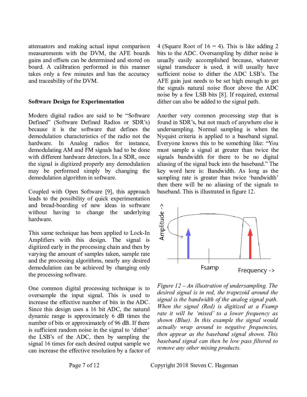
the AFE boards gains and offsets can be determined and stored on board. A calibration performed in this manner takes only a few minutes and has the accuracy and traceability of the DVM. Software Design for Experimentation Modern digital radios are said to be “Software Defined” (Software Defined Radios or SDR’s) because it is the software that defines the demodulation characteristics of the radio not the hardware. In Analog radios for instance, demodulating AM and FM signals had to be done with different hardware detectors. In a SDR, once the signal is digitized properly any demodulation may be performed simply by changing the demodulation algorithm in software. Coupled with Open Software [9], this approach leads to the possibility of quick experimentation and bread-boarding of new ideas in software without having to change the underlying hardware. This same technique has been applied to Lock-In Amplifiers with this design. The signal is digitized early in the processing chain and then by varying the amount of samples taken, sample rate and the processing algorithms, nearly any desired demodulation can be achieved by changing only the processing software. One common digital processing technique is to oversample the input signal. This is used to increase the effective number of bits in the ADC. Since this design uses a 16 bit ADC, the natural dynamic range is approximately 6 dB times the number of bits or approximately of 96 dB. If there is sufficient random noise in the signal to ‘dither’ the LSB’s of the ADC, then by sampling the signal 16 times for each desired output sample we can increase the effective resolution by a factor of 4 (Square Root of 16 = 4). This is like adding 2 bits to the ADC. Oversampling by dither noise is usually easily accomplished because, whatever signal transducer is used, it will usually have sufficient noise to dither the ADC LSB’s. The AFE gain just needs to be set high enough to get the signals natural noise floor above the ADC noise by a few LSB bits [8]. If required, external dither can also be added to the signal path. Another very common processing step that is found in SDR’s, but not much of anywhere else is undersampling. Normal sampling is when the Nyquist criteria is applied to a baseband signal. Everyone knows this to be something like: “You must sample a signal at greater than twice the signals bandwidth for there to be no digital aliasing of the signal back into the baseband.” The key word here is: Bandwidth. As long as the sampling rate is greater than twice ‘bandwidth’ then there will be no aliasing of the signals to baseband. This is illustrated in figure 12. Figure 12 – An illustration of undersampling. The desired signal is in red, the trapezoid around the signal is the bandwidth of the analog signal path. When the signal (Red) is digitized at a Fsamp rate it will be ‘mixed’ to a lower frequency as shown (Blue). In this example the signal would actually wrap around to negative frequencies, then appear as the baseband signal shown. This baseband signal can then be low pass filtered to remove any other mixing products. Page 7 of 12 Copyright 2018 Steven C. Hageman
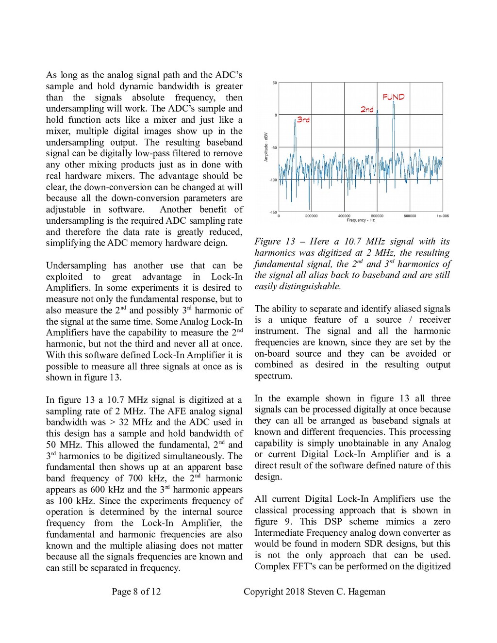
sample and hold dynamic bandwidth is greater than the signals absolute frequency, then undersampling will work. The ADC’s sample and hold function acts like a mixer and just like a mixer, multiple digital images show up in the undersampling output. The resulting baseband signal can be digitally low-pass filtered to remove any other mixing products just as in done with real hardware mixers. The advantage should be clear, the down-conversion can be changed at will because all the down-conversion parameters are adjustable in software. Another benefit of undersampling is the required ADC sampling rate and therefore the data rate is greatly reduced, simplifying the ADC memory hardware deign. Undersampling has another use that can be exploited to great advantage in Lock-In Amplifiers. In some experiments it is desired to measure not only the fundamental response, but to also measure the 2nd and possibly 3rd harmonic of the signal at the same time. Some Analog Lock-In Amplifiers have the capability to measure the 2nd harmonic, but not the third and never all at once. With this software defined Lock-In Amplifier it is possible to measure all three signals at once as is shown in figure 13. In figure 13 a 10.7 MHz signal is digitized at a sampling rate of 2 MHz. The AFE analog signal bandwidth was > 32 MHz and the ADC used in this design has a sample and hold bandwidth of 50 MHz. This allowed the fundamental, 2nd and 3rd harmonics to be digitized simultaneously. The fundamental then shows up at an apparent base band frequency of 700 kHz, the 2nd harmonic appears as 600 kHz and the 3rd harmonic appears as 100 kHz. Since the experiments frequency of operation is determined by the internal source frequency from the Lock-In Amplifier, the fundamental and harmonic frequencies are also known and the multiple aliasing does not matter because all the signals frequencies are known and can still be separated in frequency. Figure 13 – Here a 10.7 MHz signal with its harmonics was digitized at 2 MHz, the resulting fundamental signal, the 2nd and 3rd harmonics of the signal all alias back to baseband and are still easily distinguishable. The ability to separate and identify aliased signals is a unique feature of a source / receiver instrument. The signal and all the harmonic frequencies are known, since they are set by the on-board source and they can be avoided or combined as desired in the resulting output spectrum. In the example shown in figure 13 all three signals can be processed digitally at once because they can all be arranged as baseband signals at known and different frequencies. This processing capability is simply unobtainable in any Analog or current Digital Lock-In Amplifier and is a direct result of the software defined nature of this design. All current Digital Lock-In Amplifiers use the classical processing approach that is shown in figure 9. This DSP scheme mimics a zero Intermediate Frequency analog down converter as would be found in modern SDR designs, but this is not the only approach that can be used. Complex FFT’s can be performed on the digitized Page 8 of 12 Copyright 2018 Steven C. Hageman
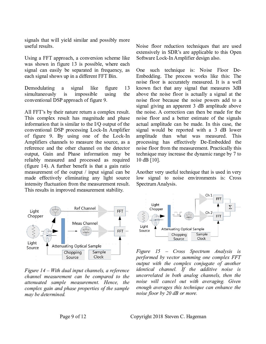
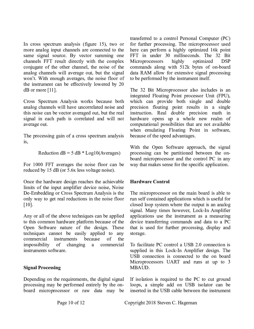
Using a FFT approach, a conversion scheme like was shown in figure 13 is possible, where each signal can easily be separated in frequency, as each signal shows up in a different FFT Bin. Demodulating a signal like figure 13 simultaneously is impossible using the conventional DSP approach of figure 9. All FFT’s by their nature return a complex result. This complex result has magnitude and phase information that is similar to the I/Q output of the conventional DSP processing Lock-In Amplifier of figure 9. By using one of the Lock-In Amplifiers channels to measure the source, as a reference and the other channel on the detector output, Gain and Phase information may be reliably measured and processed as required (figure 14). A further benefit is that a gain ratio measurement of the output / input signal can be made effectively eliminating any light source intensity fluctuation from the measurement result. This results in improved measurement stability. Figure 14 – With dual input channels, a reference channel measurement can be compared to the attenuated sample measurement. Hence, the complex gain and phase properties of the sample may be determined. Noise floor reduction techniques that are used extensively in SDR’s are applicable to this Open Software Lock-In Amplifier design also. One such technique is: Noise Floor De- Embedding. The process works like this: The noise floor is accurately measured. It is a well known fact that any signal that measures 3dB above the noise floor is actually a signal at the noise floor because the noise powers add to a signal giving an apparent 3 dB amplitude above the noise. A correction can then be made for the noise floor and a better estimate of the signals actual amplitude can be made. In this case, the signal would be reported with a 3 dB lower amplitude than what was measured. This processing has effectively De-Embedded the noise floor from the measurement. Practically this technique may increase the dynamic range by 7 to 10 dB [10]. Another very useful technique that is used in very low signal to noise environments is: Cross Spectrum Analysis. Figure 15 – Cross Spectrum Analysis is performed by vector summing one complex FFT output with the complex conjugate of another identical channel. If the additive noise is uncorrelated in both analog channels, then the noise will cancel out with averaging. Given enough averages this technique can enhance the noise floor by 20 dB or more. Page 9 of 12 Copyright 2018 Steven C. Hageman
input channels are connected to the same signal source. By vector summing one channels FFT result directly with the complex conjugate of the other channel, the noise of the analog channels will average out, but the signal won’t. With enough averages, the noise floor of the instrument can be effectively lowered by 20 dB or more [11]. Cross Spectrum Analysis works because both analog channels will have uncorrelated noise and this noise can be vector averaged out, but the real signal in each path is correlated and will not average out. The processing gain of a cross spectrum analysis is, Reduction dB = 5 dB * Log10(Averages) For 1000 FFT averages the noise floor can be reduced by 15 dB (or 5.6x less voltage noise). Once the hardware design reaches the achievable limits of the input amplifier device noise, Noise De-Embedding or Cross Spectrum Analysis is the only way to get real reductions in the noise floor [10]. Any or all of the above techniques can be applied to this common hardware platform because of the Open Software nature of the design. These techniques cannot be easily applied to any commercial instruments because of the impossibility of changing a commercial instruments software. Signal Processing Depending on the requirements, the digital signal processing may be performed entirely by the on- board microprocessor or raw data may be transferred to a control Personal Computer (PC) for further processing. The microprocessor used here can perform a highly optimized 16k point FFT in under 30 milliseconds. The 32 Bit Microprocessors highly optimized DSP commands along with 512k bytes of on-board data RAM allow for extensive signal processing to be performed by the instrument itself. The 32 Bit Microprocessor also includes is an integrated Floating Point processor Unit (FPU), which can provide both single and double precision floating point results in a single instruction. Real double precision math in hardware opens up a whole new realm of computational possibilities that are not available when emulating Floating Point in software, because of the speed advantages. With the Open Software approach, the signal processing can be partitioned between the on- board microprocessor and the control PC in any way that makes sense for the specific application. Hardware Control The microprocessor on the main board is able to run self contained applications which is useful for closed loop system where the output is an analog signal. Many times however, Lock-In Amplifier applications use the instrument as a measuring device transferring commands and data to a PC that is used for further processing, display and storage. To facilitate PC control a USB 2.0 connection is supplied in this Lock-In Amplifier design. The USB connection is connected to the on board Microprocessors UART and runs at up to 3 MBAUD. If isolation is required to the PC to cut ground loops, a simple add on USB isolator can be inserted in the USB cable between the instrument Page 10 of 12 Copyright 2018 Steven C. Hageman
powered. Control commands to the Lock-In Amplifier are processed through a SCPI like command parser [13]. For instance, a command to start a data acquisition sequence, and read the result would be: “CHANel1:MEASure?”, which can be shortened to: “CHAN1:MEAS?”. The command above would initiate a data capture on channel 1 and return the data array result. With the Open Software nature of the instrument, any command may be added or multiple operations can be combined into one as may be desired for the experiment at hand. This makes control of the instrument easy and intuitive. In SCPI a standard set of commands are always present like, *IDN?, Which asks the instrument to identify itself, *RST, Which causes the instrument to preset itself to the power on state. The command parser API is easy to extend making the addition of application specific commands straightforward. This is useful because different AFE designs will almost certainly require custom command sets for control. Wrapping the design up The hardware design was sized to fit a commercial extruded enclosure that measures 5 x 6 x 2 inches tall. The front and rear panels of this design are flat plates which allows custom front and rear panels to be easily made to fit any custom application. Using a simple hardware chassis design allows for easy access to the hardware for development and troubleshooting purposes as the hardware slides out of the chassis for access. The all aluminum enclosure also provides electrical shielding and environmental isolation from drift inducing air currents. The design with the universal JFET Input AFE consumes about 7.5 Watts total from a 9 VDC source, which leads to only a few degrees C temperature rise of the enclosure. Figure 16 – The experimental Lock-In Amplifier design fits in a 5 x 6 x 2 inch tall commercial enclosure. Notes / References [1] Robert H. Dicke, Physicist, Popularized the Lock-In Amplifier. https://en.wikipedia.org/wiki/Robert_H._Dicke [2] Even chopper amplifiers have 1/f noise. Though choppers are better than other types of amplifiers, their noise will eventually have a 1/f shape if you look at a low enough frequency. [3] The best analog switching circuits available Page 11 of 12 Copyright 2018 Steven C. Hageman
of the very fast and low capacitance DMOS switches like the Siliconix (now Vishay) SD210 series which are still available today. [4] Some ‘advanced’ Analog Lock-In Amplifiers implemented a quasi-sine wave demodulator based on the Walsh function and implemented with a 4 step quantized sinewave multiplier. These designs had the effect of reducing the odd harmonic responses about 20 dB from their square wave based counterparts. See: Princeton Applied Research Model 5210. [5] This is interesting, because the same Analog Dialog Magazine that introduced an IC form of figure 5, the AD630, also had articles on DSP based chips and methods that could duplicate these analog functions digitally. See: Analog Dialog V17n1, 1983. The AD630 is limited to demodulation frequencies of less than 200 kHz. [6] Analog Devices ADA2200 a more modern Lock-In Amplifier chip. [7] See Hewlett Packard Journals, HP434A, Vol 9 No 12, August 1958 HP431A, Vol 12 No 10, June 1961 HP436A, Vol 27 No 2, October 1975 The most modern design to use a Lock-In Amplifier technique is the Keysight E4416A. [8] The rule of thumb here is that for oversampling to work well that the random noise that dithers or modulates the ADC LSB’s should be a couple of bits or at least: 2 * 6 dB = 12 dB above the natural ADC noise floor. The noise should have a normal distribution. Usually the signal transducers and AFE amplifier noise and gain can be adjusted to meet this goal. Sometimes extra dither is added to the circuit directly ahead of the ADC. [9] “Open Software” is defined here as: Source code that you have access to and can modify as needed. This is in contrast to “Closed Software” as would be found inside a typical commercial instrument. There is no way to modify Closed Software to meet your needs because you don’t have access to it. [10] Hageman, Steve. “Measuring Small Signals Accurately”, EDN August 23, 2012. https://www.edn.com/design/test-and- measurement/4394635/Measuring-small-signals- accurately--A-practical-guide [11] Eventually the analog channel noise will become correlated at low enough levels due to crosstalk leakage, power supply coupling or thermal drift and the averaging will cease to be effective. Practically, I find this to happen at -20 to -30 dB reduction in the noise floor, unless extreme care is taken in de-coupling every aspect of the hardware design. [12] USB isolators based on the Analog Devices ADuM4160 can be found on-line at very reasonable prices. These isolators can be very effective at reducing ground loop noise and providing leakage current isolation in USB connections. [13] SCPI stands for: “Standard Commands for Programmable Instruments” and is a human readable, mnemonic based syntax that is used extensively to control instruments. http://www.ivifoundation.org/scpi/ Author Information: Steve Hageman is a confirmed “Analog-aholic” having fallen ill to the disease in about the 5th grade. Since then he has designed and built all sorts of Analog and RF equipment spanning DC to 50 GHz. Currently he designs custom instrumentation for all sorts of interesting projects. Page 12 of 12 Copyright 2018 Steven C. Hageman
![and the PC [12] and the instrument may be battery](https://files.speakerdeck.com/presentations/6a7d0a7c454b4954b1aee73a01de6095/slide_10.jpg)