Upgrade to Pro — share decks privately, control downloads, hide ads and more …

[2/6] Seebeck coefficient

[2/6] Seebeck coefficient

Andrei Novitskii

March 16, 2021
Tweet

More Decks by Andrei Novitskii

Other Decks in Education

Transcript

  1. Лекция «Введение в физику полупроводников» / 24 января 2024 г.

    2 Fermi integral and Seebeck coefficient The 𝑗-th order Fermi integrals, 𝐹𝑗 𝜂 , defined by 𝐹𝑗 𝜂 = න 0 ∞ 𝜀𝑗 1 + 𝑒𝜀−𝜂 𝑑𝜀 here 𝑗 is the order of integral, 𝜂 is the reduced Fermi energy (chemical potential), 𝜀 is the reduced carrier energy.[1] The experimental transport data can be analyzed using a common solution to the Boltzmann transport equation within the relaxation time approximation. It is assumed that electron conduction occurs within a single parabolic band (SPB) with a single scattering mechanism where the energy dependence of the carrier relaxation time can be expressed by a simple power-law 𝜏 = 𝜏0 𝐸𝑟. The Seebeck coefficient derived from the Boltzmann transport equations within SPB model provided as follows[2] 𝛼 𝜂 = ± 𝑘𝐵 𝑒 𝑟 + Τ 5 2 𝐹𝑟+ Τ 3 2 𝜂 𝑟 + Τ 3 2 𝐹𝑟+ Τ 1 2 𝜂 − 𝜂 here 𝑘𝐵 is the Boltzmann constant, 𝑟 is the scattering parameter related to the energy dependence of the carrier relaxation time, 𝜏. 𝜂 could be obtained via analysis of the Seebeck coefficient data.
  2. Лекция «Введение в физику полупроводников» / 24 января 2024 г.

    3 Seebeck coefficient 𝛼 𝜂 = ± 𝑘𝐵 𝑒 𝑟 + Τ 5 2 𝐹𝑟+ Τ 3 2 𝜂 𝑟 + Τ 3 2 𝐹𝑟+ Τ 1 2 𝜂 − 𝜂
  3. Лекция «Введение в физику полупроводников» / 24 января 2024 г.

    4 Seebeck coefficient 𝛼 𝜂 = ± 𝑘𝐵 𝑒 𝑟 + Τ 5 2 𝐹𝑟+ Τ 3 2 𝜂 𝑟 + Τ 3 2 𝐹𝑟+ Τ 1 2 𝜂 − 𝜂 degenerate limit 𝜂 > 5 non-degenerate limit 𝜂 < −1 The Fermi integral can be approximated for different regions of 𝜂. For example, for 𝐹 Τ 1 2 𝜂 : 𝐹 Τ 1 2 𝜂 = 𝜋 2 𝑒𝜂, −∞ < 𝜂 < −1 𝜋 2 1 Τ 1 4 + 𝑒−𝜂 , −1 < 𝜂 < 5 2 3 𝜂 Τ 3 2, 5 < 𝜂 < ∞
  4. In the same manner, the Seebeck coefficient can be also

    approximated for two situations[3,4] Reminder: for p-type semiconductors 𝛼 > 0, for n-type semiconductors 𝛼 < 0, when 𝑟 = − Τ 1 2 (deformation scattering potential) 𝑚𝑆 ∗ ≈ 𝑚𝑑 ∗ . For metals 𝛼 = 𝜋2 3 𝑘𝐵 2𝑇 𝑒 𝜕 log𝜎 𝐸 𝜕𝐸 𝐸=𝐸𝐹 and thus, in the neighborhood of 𝐸 = 𝐸𝐹, 𝜎 𝐸 = const ∙ 𝐸𝑟, this becomes 𝛼 = 𝜋2 3 𝑘𝐵 2𝑇 𝑒𝐸𝐹 𝑟.[6] This formula is known as Mott relation and valid for all metals and alloys at 𝑇 > 𝜃𝐷. Лекция «Введение в физику полупроводников» / 24 января 2024 г. 5 Seebeck coefficient degenerate limit 𝛼 𝜂 = ± 𝜋2 3 𝑘𝐵 𝑒 3 2 + 𝑟 1 𝜂 Thus 𝛼 = ± 8𝜋2𝑘𝐵 2𝑇 3𝑒ℎ2 𝑚𝑆 ∗ 𝜋 3𝑛 Τ 2 3 3 2 + 𝑟 non-degenerate limit 𝛼 𝜂 = ± 𝑘𝐵 𝑒 5 2 + 𝑟 − 𝜂 thus 𝛼 = ± 𝑘𝐵 𝑒 5 2 + 𝑟 + ln 2 ൗ 2𝜋𝑚𝑆 ∗𝑘𝐵 𝑇 ℎ2 3/2 𝑛 ∗ *known as Pisarenko relation[2,5]
  5. Лекция «Введение в физику полупроводников» / 24 января 2024 г.

    6 Seebeck coefficient 𝛼 𝜂 = ± 𝑘𝐵 𝑒 𝑟 + Τ 5 2 𝐹𝑟+ Τ 3 2 𝜂 𝑟 + Τ 3 2 𝐹𝑟+ Τ 1 2 𝜂 − 𝜂 in the case of deformation potential (acoustic phonon scattering) 𝑟 = − Τ 1 2 and thus, 𝛼 𝜂 = ± 𝑘𝐵 𝑒 2𝐹1 𝜂 𝐹0 𝜂 − 𝜂 degenerate limit: 𝛼 𝜂 = ± 𝜋2 3 𝑘𝐵 𝑒 1 𝜂 non-degenerate limit: 𝛼 𝜂 = ± 𝑘𝐵 𝑒 2 − 𝜂 𝑘𝐵 𝑒 2𝐹1 𝜂 𝐹0 𝜂 − 𝜂 𝜋2 3 𝑘𝐵 𝑒 1 𝜂 𝑘𝐵 𝑒 2 − 𝜂
  6. Лекция «Введение в физику полупроводников» / 24 января 2024 г.

    7 Parabolic bands are not real? Degenerate limit: 𝛼 = ± 8𝜋2𝑘𝐵 2𝑇 3𝑒ℎ2 𝑚𝑆 ∗ 𝜋 3𝑛 Τ 2 3 3 2 + 𝑟 Degenerate limit for Kane dispersion: 𝛼 = ± 8𝜋2𝑘𝐵 2𝑇 3𝑒ℎ2 𝑚𝑆 ∗ 𝜋 3𝑛 Τ 2 3 3 2 + 𝑟 − 𝜙 correction factor: 𝜙 = ൘ 4𝐸 𝐸𝑔 1+ ൗ 𝐸 𝐸𝑔 1+ ൗ 2𝐸 𝐸𝑔 2 and 𝑚𝑆 ∗ = 𝑚0 ∗ 1 + ൗ 2𝐸 𝐸𝑔 See Ref. [7]
  7. Лекция «Введение в физику полупроводников» / 24 января 2024 г.

    8 Parabolic bands are not real? Degenerate limit: 𝛼 = ± 8𝜋2𝑘𝐵 2𝑇 3𝑒ℎ2 𝑚𝑆 ∗ 𝜋 3𝑛 Τ 2 3 3 2 + 𝑟 Degenerate limit for Kane dispersion: 𝛼 = ± 8𝜋2𝑘𝐵 2𝑇 3𝑒ℎ2 𝑚𝑆 ∗ 𝜋 3𝑛 Τ 2 3 3 2 + 𝑟 − 𝜙 correction factor: 𝜙 = ൘ 4𝐸 𝐸𝑔 1+ ൗ 𝐸 𝐸𝑔 1+ ൗ 2𝐸 𝐸𝑔 2 and 𝑚𝑆 ∗ = 𝑚0 ∗ 1 + ൗ 2𝐸 𝐸𝑔 See Ref. [7]
  8. Лекция «Введение в физику полупроводников» / 24 января 2024 г.

    12 Parabolic bands are not real? 𝛼 = ± 8𝜋2𝑘𝐵 2𝑇 3𝑒ℎ2 𝑚𝑆 ∗ 𝜋 3𝑛 Τ 2 3
  9. 𝐿 𝜂 = 𝑘𝐵 𝑒 2 𝑟 + Τ 7

    2 𝐹𝑟+ Τ 5 2 𝜂 𝑟 + Τ 3 2 𝐹𝑟+ Τ 1 2 𝜂 − 𝑟 + Τ 5 2 𝐹𝑟+ Τ 3 2 𝜂 𝑟 + Τ 3 2 𝐹𝑟+ Τ 1 2 𝜂 2 Degenerate limit: 𝐿 = 𝜋2 3 𝑘𝐵 𝑒 2 = 2.45 ∙ 10−8 V2 K2 Non-degenerate limit: 𝐿 = 2 𝑘𝐵 𝑒 2 = 1.49 ∙ 10−8 V2 K2 Reasonable approximation 𝐿 = 1.5 + 𝑒− Τ 𝛼 116 (see Ref. [9]) Intrinsic region: 𝐿 = 𝑘𝐵 𝑒 2 𝑟 + 5 2 + 2 𝑟 + 1 2 + 𝑒𝐸𝑔 𝑘𝐵𝑇 2 𝑏 1+𝑏 2 , 𝑏 = Τ 𝜇𝑛 𝜇𝑝 and 1 + 𝑏 = 𝜎𝑛 + 𝜎𝑝 = 𝜎 at high temperatures 𝑏 = 1 Лекция «Введение в физику полупроводников» / 24 января 2024 г. 13 Lorenz number
  10. In the framework of the effective mass model (also called

    single parabolic band model) chemical (real) charge carrier concentration is defined as[1,2] 𝑛 𝜂 = 4𝜋 2𝑚𝑑 ∗ 𝑘𝐵 𝑇 ℎ2 Τ 3 2 𝐹1/2 𝜂 It should be considered that the Hall charge carrier concentration is related to the chemical one via 𝑛 = 𝑛𝐻 𝑟𝐻, where 𝑟𝐻 is the Hall factor given by[1,2] 𝑟𝐻 𝜂 = 3 2 𝐹 Τ 1 2 𝜂 3 2 + 2𝑟 𝐹2𝑟+ Τ 1 2 𝜂 3 2 + 𝑟 2 𝐹 𝑟+ Τ 1 2 2 𝜂 For complete degeneracy (𝜂 > 5) 𝑟𝐻 = 1 regardless of the scattering mechanism. For non- degenerate semiconductors (𝜂 < – 1) 𝑟𝐻 = Τ 315𝜋 512 = 1.93 for ionized impurities scattering (𝑟 = Τ 3 2), 𝑟𝐻 = Τ 45𝜋 128 = 1.13 for polar optical phonon scattering (𝑟 = Τ 1 2), 𝑟𝐻 = 1 for charge- neutral impurity scattering (𝑟 = 0) and 𝑟𝐻 = Τ 3𝜋 8 = 1.18 for a scattering of carries via acoustic phonons (𝑟 = Τ −1 2).[2,10] Лекция «Введение в физику полупроводников» / 24 января 2024 г. 14 Carrier concentration and Hall factor
  11. For non-degenerate region, the Hall factor can be approximated as

    follows 𝑟𝐻 = Γ 5 2 Γ 5 2 + 2𝑟 Γ 5 2 + 𝑟 2 For example, in the case of acoustic phonon scattering (𝑟 = − 1 2 ): 𝑟𝐻 𝜂 = 3 4 𝐹 Τ 1 2 𝜂 𝐹− Τ 1 2 𝜂 𝐹0 2 𝜂 degenerate limit 𝑟𝐻 = 1 non-degenerate limit 𝑟𝐻 = Γ 5 2 Γ 3 2 Γ 2 2 = 3𝜋 8 = 1.18 Лекция «Введение в физику полупроводников» / 24 января 2024 г. 15 Hall factor
  12. Лекция «Введение в физику полупроводников» / 24 января 2024 г.

    16 Effective mass calculation If the Hall measurements were carried out, the effective mass can be calculated directly from 𝑛 𝜂 = 4𝜋 2𝑚𝑑 ∗ 𝑘𝐵𝑇 ℎ2 Τ 3 2 𝐹𝑟+1 𝜂 . Another possible trick is to calculate the effective mass by using experimental values of the Seebeck coefficient: 𝛼 = ± 8𝜋2𝑘𝐵 2𝑇 3𝑒ℎ2 𝑚𝑆 ∗ 𝜋 3𝑛 Τ 2 3 3 2 + 𝑟 . In the framework of the single parabolic band model (SPB) the effective mass is expected to be a constant with changes in carrier concentration or Fermi level. Thus, the plot of 𝛼 as a function of 𝑛 can be used to evaluate how well your data fit the SPB model.
  13. If the Hall measurements were carried out, the effective mass

    can be calculated directly from 𝑛 𝜂 = 4𝜋 2𝑚𝑑 ∗ 𝑘𝐵𝑇 ℎ2 Τ 3 2 𝐹𝑟+1 𝜂 . Another possible trick is to calculate the effective mass by using experimental values of the Seebeck coefficient: 𝛼 = ± 8𝜋2𝑘𝐵 2𝑇 3𝑒ℎ2 𝑚𝑆 ∗ 𝜋 3𝑛 Τ 2 3 3 2 + 𝑟 . In the framework of the single parabolic band model (SPB) the effective mass is expected to be a constant with changes in carrier concentration or Fermi level. Thus, the plot of 𝛼 as a function of 𝑛 can be used to evaluate how well your data fit the SPB model. Лекция «Введение в физику полупроводников» / 24 января 2024 г. 17 Effective mass calculation Degenerate limit SPB-APS model
  14. Several common equations for the Seebeck coefficient assume the transport

    function has a narrow width, e.g., conducting electrons all have similar energy (band is narrower than 𝑘𝐵 𝑇). This means 𝑓(𝐸) ~ 𝑓(𝐸𝑏 ) is a constant. 𝛼𝜎 = − 1 𝑒𝑇 ׬ 𝜎𝑒 𝐸 − 𝐹 𝜕𝑓 𝜕𝐸 𝑑𝐸 𝑓 𝐸, 𝑇 = 1 𝑒 𝐸−𝐹 𝑘𝐵𝑇+1 𝜕𝑓 𝐸,𝑇 𝜕𝐸 = −𝑓2𝑒 𝐸−𝐹 𝑘𝐵𝑇 1 𝑘𝐵𝑇 𝛼 = 𝐸𝑏−𝐹 𝑒𝑇 Лекция «Введение в физику полупроводников» / 24 января 2024 г. 18 Narrow band Seebeck 𝑘𝐵 𝑇
  15. The narrow band formula is also often used for intrinsic

    semiconductors and amorphous materials even though the bands are not narrow. 𝛼 = 𝐸𝑏 − 𝐹 𝑒𝑇 + 𝐴 where 𝐴 = ׬ 𝐸 − 𝐸𝑏 𝜎𝐸 𝜕𝑓 𝜕𝐸 𝑑𝐸 𝑒𝑇 ׬ 𝜎𝐸 𝜕𝑓 𝜕𝐸 𝑑𝐸 𝐴 contains all the difficult integration, so it is helpful only when 𝐴 is reasonably small. In a normal band 𝐴 is the Seebeck coefficient when 𝐸𝑏 = 𝐹 at the band edge, approximately 200 µV·K–1. This is not negligible for normal metals or semiconductors. 𝐴 is small only in large band gap insulators, where the Fermi level is so far from the transport edge (many 𝑘𝐵 𝑇) that the 𝛼 ≫ 200 µV·K–1. For intrinsic semiconductors: 𝛼~ln 1 𝑛 with 𝑛 = 2 𝑚∗𝑘𝐵𝑇 2𝜋ℏ2 Τ 3 2 𝑒− 𝐸𝑏−𝐹 𝑘𝐵𝑇 Лекция «Введение в физику полупроводников» / 24 января 2024 г. 19 Narrow band Seebeck
  16. The Heikes formula is commonly used to describe narrow band

    insulators, such as materials with localized 𝑑 or 𝑓 state electrons or other strongly correlated electron materials. As was shown already for carrier concentration: band at 𝐸𝑏 has total states 𝑁 = ׬ 𝑔 𝐸 𝑑𝐸 and thus number of electrons or filled states 𝑛 = ׬ 𝑓 𝐸, 𝑇 𝑔 𝐸 𝑑𝐸. Then, fraction of filled states is equal to the Fermi function evaluated at the band: 𝑐 = 𝑓 𝐸𝑏 , 𝑇 = 1 𝑒 𝐸𝑏−𝐹 𝑘𝐵𝑇 +1 = 𝑛 𝑁 , so, quite easy we can get that 𝐸𝑏−𝐹 𝑘𝐵𝑇 = ln 1−𝑐 𝑐 . Considering that 𝛼 = 𝐸𝑏−𝐹 𝑒𝑇 , the Seebeck can be represented as 𝛼 = 𝑘𝐵 𝑒 ln 1 − 𝑐 𝑐 Лекция «Введение в физику полупроводников» / 24 января 2024 г. 20 Narrow band Seebeck. Heikes formula Narrow conduction band Narrow valence band
  17. Лекция «Введение в физику полупроводников» / 24 января 2024 г.

    21 Seebeck coefficient and configurational entropy Considering that 𝛼 = 𝑘𝐵 𝑒 ln 1−𝑐 𝑐 and 𝑐 = 𝑛 𝑁 , where 𝑛 is the number of filled states, while 𝑁 is the total number of states, the Seebeck coefficient may be related to the configurational entropy: 𝛼 = 𝑘𝐵 𝑒 𝜕lnΩ 𝜕𝑛 where Ω = 𝑁! 𝑁−𝑛 !𝑛! for 𝑛 particles in 𝑁 states. Thus, the Seebeck coefficient can be considered as the change in entropy with number of particles: small 𝑛 and many more configurations → large 𝛼 over half full, Ω decrease, 𝛼 sign change larger 𝑛 up to half full, less Ω increase, small 𝛼 (see Figure)
  18. The Heikes formula is temperature independent because the Fermi level

    is adjusted at each temperature to make sure the fraction of filled states determined by the chemical composition is a constant. For instance, to evaluate the contributions of spin orbital entropy, the Seebeck coefficient enhancement can be estimated via so-called modified Heikes formula: 𝛼 = − 𝑘𝐵 𝑒 ln 𝑔𝑛 𝑔𝑛+1 𝑥𝑛+1 1 − 𝑥𝑛+1 where 𝑔𝑛 and 𝑔𝑛+1 are the number the spin-orbital configurations of the 𝑀𝑛+ and 𝑀 𝑛+1 + ions, 𝑥 is the concentration of 𝑀 𝑛+1 + ions. For more details see Ref. [11,12]. Лекция «Введение в физику полупроводников» / 24 января 2024 г. 22 Heikes formula. Example
  19. For non-degenerate semiconductors Jonker proposed following relation between the Seebeck

    coefficient and the electrical conductivity:[13,14] 𝛼 = ± 𝑘𝐵 𝑒 𝑏 − ln𝜎 here, parameter 𝑏 involves 𝜇𝑤 𝑇 Τ 3 2 term, where 𝜇𝑤 is the weighted mobility (will be discussed in the next lecture). The Jonker plot (see Figure) with a constant slope of ± 𝑘𝐵 𝑒 describes the behavior of an ideal single-parabolic band semiconductor. Combined with the so-called Ioffe analysis can be used for 𝛼2𝜎 max prediction. For details see Ref. [15]. Лекция «Введение в физику полупроводников» / 24 января 2024 г. 23 Jonker-type analysis Example for Bi1–x Lax CuSeO (x = 0, 0.02, 0.04, 0.06, 0.08)
  20. Лекция «Введение в физику полупроводников» / 24 января 2024 г.

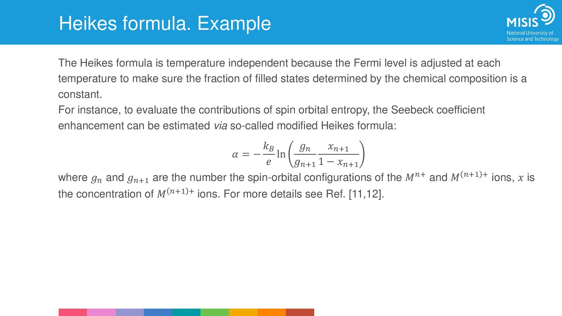
    24 References 1. Kireev, P.S. Semiconductor Physics, 2nd ed.; Mir: Moscow, 1978. 2. Fistul’, V.I. Heavily Doped Semiconductors; Springer New York: Boston, MA, 1995. 3. Materials, Preparation, and Characterization in Thermoelectrics; Rowe, D.M., Ed.; CRC Press, 2012. 4. Bonch-Bruevich, V.L.; Kalashnikov, S.G. Semiconductor Physics; Nauka: Moscow, 1977. 5. Ioffe, A.F. Semiconductor Thermoelements, and Thermoelectric Cooling; Infosearch: London, 1957. 6. Mott, N.F.; Jones, H. The Theory of the Properties of Metals and Alloys; Dover Publications: New York, 1958. 7. Tang, Y.; Gibbs, Z.M.; Agapito, L.A.; Li, G.; Kim, H.-S.; Nardelli, M.B.; Curtarolo, S.; Snyder, G.J. Convergence of Multi-Valley Bands as the Electronic Origin of High Thermoelectric Performance in CoSb3 Skutterudites. Nat. Mater. 2015, 14 (12), 1223–1228. 8. Naithani, H.; Dasgupta, T. Critical Analysis of Single Band Modeling of Thermoelectric Materials. ACS Appl. Energy Mater. 2020, 3 (3), 2200–2213. 9. Kim, H.-S.; Gibbs, Z.M.; Tang, Y.; Wang, H.; Snyder, G.J. Characterization of Lorenz Number with Seebeck Coefficient Measurement. APL Mater. 2015, 3 (4), 041506.
  21. Лекция «Введение в физику полупроводников» / 24 января 2024 г.

    25 References 10. Askerov, B.M. Electron Transport Phenomena in Semiconductors; World scientific, 1994. 11. Koshibae, W.; Tsutsui, K.; Maekawa, S. Thermopower in Cobalt Oxides. Phys. Rev. B 2000, 62 (11), 6869–6872. 12. Terasaki, I. High-Temperature Oxide Thermoelectrics. J. Appl. Phys. 2011, 110 (5), 053705. 13. Jonker, G.H. The Application of Combined Conductivity and Seebeck-Effect Plots for the Analysis of Semiconductor Properties (Conductivity vs Seebeck Coefficient Plots for Analyzing n-Type, p-Type and Mixed Conduction Semiconductors Transport Properties). Philips Res. Reports 1968, 23, 131–138. 14. Rowe, D.M.; Min, G. An Alpha-Ln Sigma Plot as a Thermoelectric Material Performance Indicator. J. Mater. Sci. Lett. 1995, 14 (9), 617–619. 15. Zhu, Q.; Hopper, E.M.; Ingram, B.J.; Mason, T.O. Combined Jonker and Ioffe Analysis of Oxide Conductors and Semiconductors. J. Am. Ceram. Soc. 2011, 94 (1), 187–193. This work was inspired by brilliant course on Principles of Thermoelectric Materials Engineering by prof. Jeffrey G. Snyder (Northwestern University, USA) in the framework of On-Demand Seminar “Introduction to Thermoelectric Conversion” (February 2021).