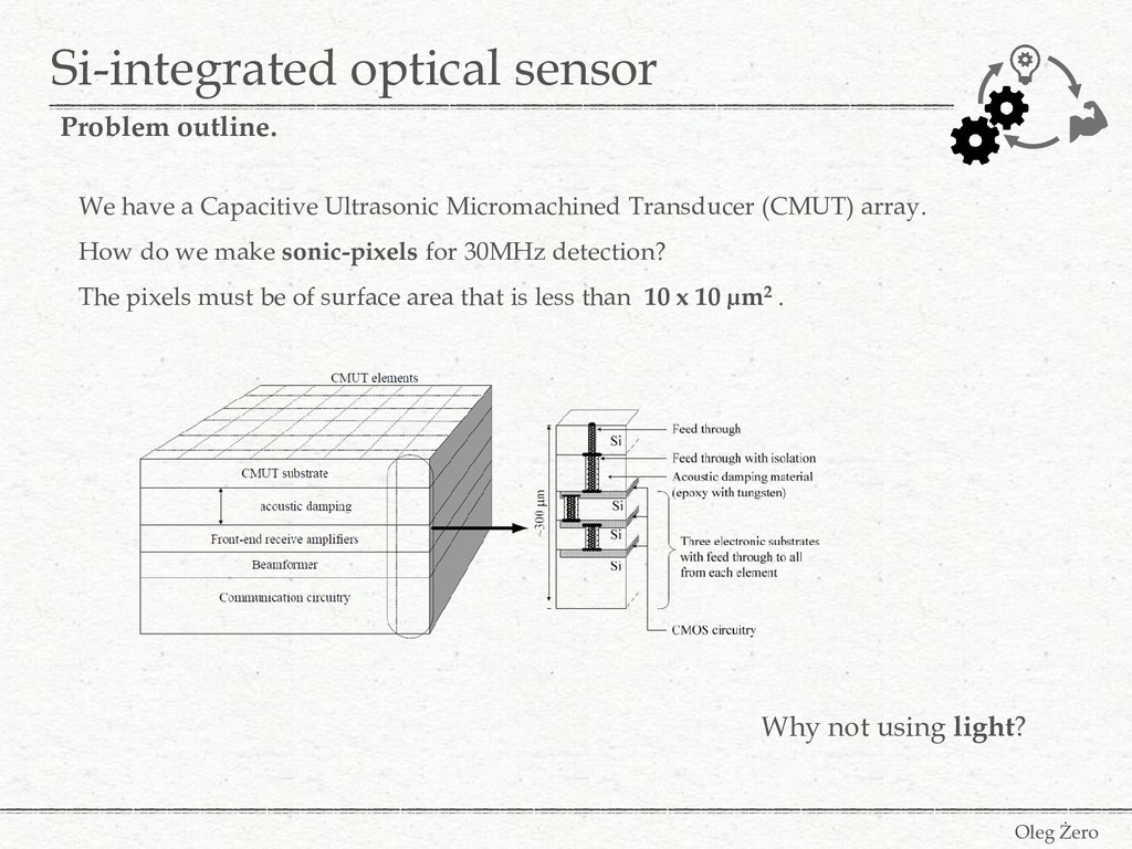
do we make sonic-pixels for 30MHz detection? The pixels must be of surface area that is less than 10 x 10 µm2 . Si-integrated optical sensor Oleg Żero Problem outline. Why not using light?
use gratings. Use Silicon-on-Insulator (SOI) technology for high index contast. Low loss at λ = 1.55 μm. Silicon will be harmless for human body (intravascular applications in mind).
use gratings. Use Silicon-on-Insulator (SOI) technology for high index contast. Low loss at λ = 1.55 μm. Silicon will be harmless for human body (intravascular applications in mind). x y x y’ x y z x y x y’ Grating to couple the light out, which will reflect by a membrane, and interfere with the evanescently coupled beam.
compact architectures. Use Silicon-on-Insulator (SOI) technology for high index contast. Low loss at λ = 1.55 μm. Silicon will be harmless for human body (intravascular applications in mind). Grating-based mechanism was hardly scalable...
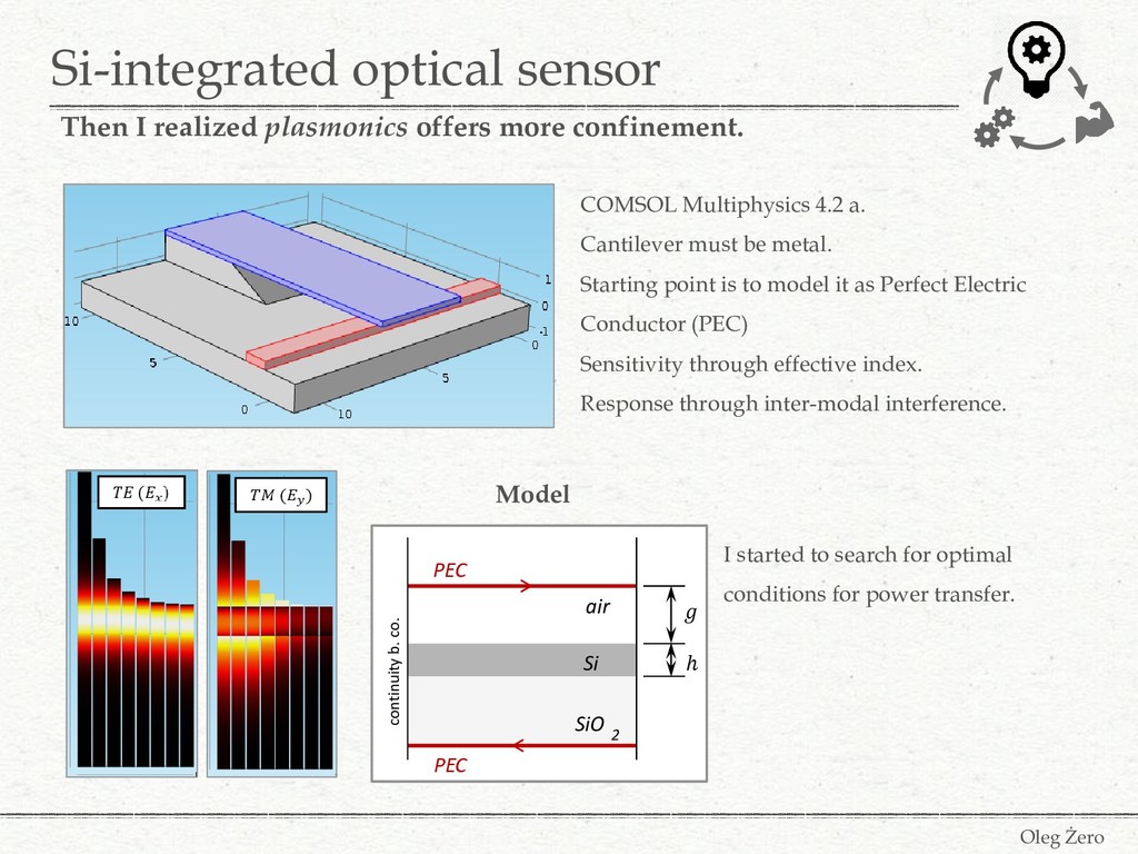
more confinement. COMSOL Multiphysics 4.2 a. Cantilever must be metal. Starting point is to model it as Perfect Electric Conductor (PEC) Sensitivity through effective index. Response through inter-modal interference. SiO 2 Si air continuity b. co. PEC PEC Model I started to search for optimal conditions for power transfer.
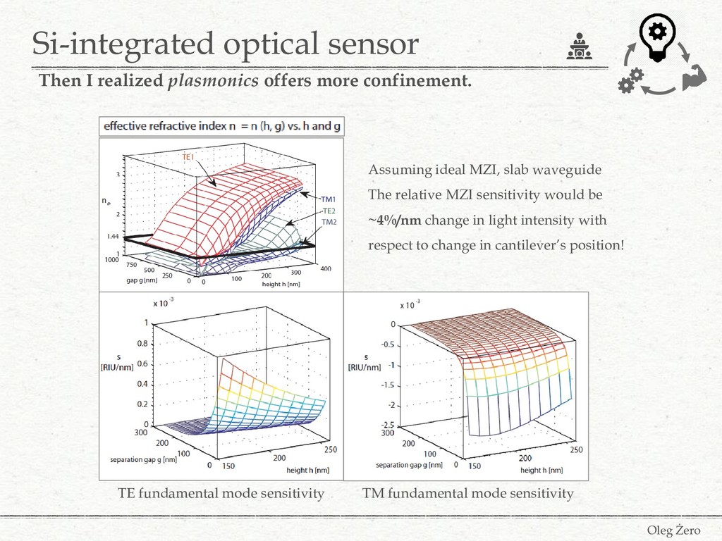
more confinement. Assuming ideal MZI, slab waveguide The relative MZI sensitivity would be ~4%/nm change in light intensity with respect to change in cantilever’s position! TE fundamental mode sensitivity TM fundamental mode sensitivity
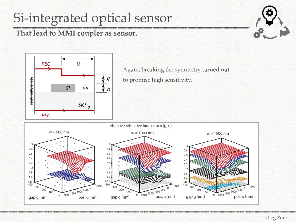
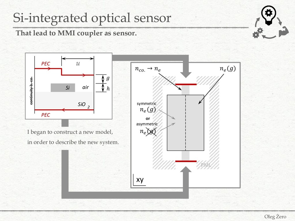
as sensor. I began to construct a new model, in order to describe the new system. SiO 2 Si air continuity b. co. PEC PEC u xy xy symmetric or asymmetric PML
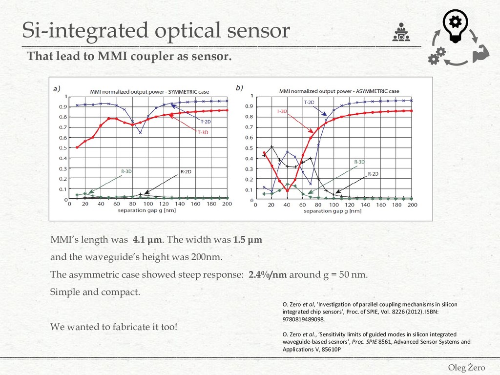
as sensor. MMI’s length was 4.1 μm. The width was 1.5 μm and the waveguide’s height was 200nm. The asymmetric case showed steep response: 2.4%/nm around g = 50 nm. Simple and compact. We wanted to fabricate it too! O. Zero et al, ‘Investigation of parallel coupling mechanisms in silicon integrated chip sensors’, Proc. of SPIE, Vol. 8226 (2012). ISBN: 9780819489098. O. Zero et al., ‘Sensitivity limits of guided modes in silicon integrated waveguide-based sesnors’, Proc. SPIE 8561, Advanced Sensor Systems and Applications V, 85610P
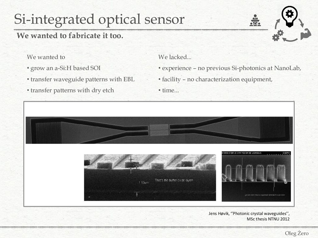
too. Jens Høvik, ‘’Photonic crystal waveguides’’, MSc thesis NTNU 2012 We wanted to • grow an a-Si:H based SOI • transfer waveguide patterns with EBL • transfer patterns with dry etch We lacked... • experience – no previous Si-photonics at NanoLab, • facility – no characterization equipment, • time...
I have... • Spent 2.5 years out of 4 in the programme. • Have 2 conferences. • Spent 9 months just teaching students. • Spent 6 months in the clean room just getting started. • None of my older colleagues has finished the programme (even now!)