Upgrade to Pro — share decks privately, control downloads, hide ads and more …

Key Structural and Chemical Features of Defect-Tolerant Semiconductors

Prashun Gorai
September 10, 2018

Key Structural and Chemical Features of Defect-Tolerant Semiconductors

Invited talk at the International Conference on Ternary and Multinary Compounds (ICTMC) in Boulder, Colorado (USA).

Prashun Gorai

September 10, 2018
Tweet

More Decks by Prashun Gorai

Other Decks in Science

Transcript

  1. Prashun Gorai, Rachel Kurchin, Tonio Buonassisi, Vladan Stevanovic Colorado School

    of Mines (CSM), National Renewable Energy Laboratory (NREL) Massachusetts Institute of Technology (MIT) Key Structural and Chemical Features of Defect-Tolerant Semiconductors GaAs deep states VB bonding anti- bonding VB CB CB MAPbI3 shallow states I(p) As(p) Pb(p) Ga(s) Pb(s) Defect-intolerant Defect-tolerant
  2. Shallow Defect States Reduce Trap-Assisted Recombination VB ET Ei trap

    CB e- h+ • Shockley-Read-Hall trap-assisted recombination rate1,2: shallow traps are desirable for defect tolerance • Recombination rate increases as ET - Ei decreases • Other factors: capture cross-section, carrier mobility, trap density n, p = electron, hole concentrations, ni = intrinsic concentration NT = trap density, vth = thermal velocity, = capture cross-section USRH = pn n2 i p + n + 2ni cosh Ei ET kT NT vth <latexit sha1_base64="R6DCV0DMPEJolrgMQ+JuKT5LMVI=">AAACznicbVHbattAEF2rtzS9xEkf+7LUFBySGMkU2pdAaBuSh1Lcxk4MliPW65G1eLUSuyMTs4i+9sP6E/2FvrYf0JXtQux0YOFw5szMzplRLoVB3/9Z8+7df/Dw0dbj7SdPnz3fqe/uXZqs0Bx6PJOZ7o+YASkU9FCghH6ugaUjCVej6YcqfzUDbUSmujjPYZiyiRKx4AwdFdWve1GYMkx0ai++npf0mIaxZtzm6khF4rpd2vxAHbQd5plJQgkxNpeK00jQI3oadUs77ZahFpME98vPUXcWWUzK0IhJyqJ6w2/5i6B3QbACDbKKTrRb64fjjBcpKOSSGTMI/ByHlmkUXEK5HRYGcsanbAIDBxVLwQztwoiSvnbMmMaZdk8hXbC3KyxLjZmnI6esljabuYr8X25QYPxuaIXKCwTFl4PiQlLMaOUqHQsNHOXcAca1cH+lPGHOJnTer01Z9M6Br21ibwrlDB7DBivxBjVzpAFMmVDVVvZMSEkvmDL/eNewSjQ/iolAc/jJnVYdnmmA6f4tMXW3CDadvwsu263AbwVf3jRO3q+uskVeklekSQLylpyQc9IhPcLJD/KL/CZ/vI4380rv21Lq1VY1L8haeN//As0A5L0=</latexit> <latexit sha1_base64="R6DCV0DMPEJolrgMQ+JuKT5LMVI=">AAACznicbVHbattAEF2rtzS9xEkf+7LUFBySGMkU2pdAaBuSh1Lcxk4MliPW65G1eLUSuyMTs4i+9sP6E/2FvrYf0JXtQux0YOFw5szMzplRLoVB3/9Z8+7df/Dw0dbj7SdPnz3fqe/uXZqs0Bx6PJOZ7o+YASkU9FCghH6ugaUjCVej6YcqfzUDbUSmujjPYZiyiRKx4AwdFdWve1GYMkx0ai++npf0mIaxZtzm6khF4rpd2vxAHbQd5plJQgkxNpeK00jQI3oadUs77ZahFpME98vPUXcWWUzK0IhJyqJ6w2/5i6B3QbACDbKKTrRb64fjjBcpKOSSGTMI/ByHlmkUXEK5HRYGcsanbAIDBxVLwQztwoiSvnbMmMaZdk8hXbC3KyxLjZmnI6esljabuYr8X25QYPxuaIXKCwTFl4PiQlLMaOUqHQsNHOXcAca1cH+lPGHOJnTer01Z9M6Br21ibwrlDB7DBivxBjVzpAFMmVDVVvZMSEkvmDL/eNewSjQ/iolAc/jJnVYdnmmA6f4tMXW3CDadvwsu263AbwVf3jRO3q+uskVeklekSQLylpyQc9IhPcLJD/KL/CZ/vI4380rv21Lq1VY1L8haeN//As0A5L0=</latexit> <latexit sha1_base64="R6DCV0DMPEJolrgMQ+JuKT5LMVI=">AAACznicbVHbattAEF2rtzS9xEkf+7LUFBySGMkU2pdAaBuSh1Lcxk4MliPW65G1eLUSuyMTs4i+9sP6E/2FvrYf0JXtQux0YOFw5szMzplRLoVB3/9Z8+7df/Dw0dbj7SdPnz3fqe/uXZqs0Bx6PJOZ7o+YASkU9FCghH6ugaUjCVej6YcqfzUDbUSmujjPYZiyiRKx4AwdFdWve1GYMkx0ai++npf0mIaxZtzm6khF4rpd2vxAHbQd5plJQgkxNpeK00jQI3oadUs77ZahFpME98vPUXcWWUzK0IhJyqJ6w2/5i6B3QbACDbKKTrRb64fjjBcpKOSSGTMI/ByHlmkUXEK5HRYGcsanbAIDBxVLwQztwoiSvnbMmMaZdk8hXbC3KyxLjZmnI6esljabuYr8X25QYPxuaIXKCwTFl4PiQlLMaOUqHQsNHOXcAca1cH+lPGHOJnTer01Z9M6Br21ibwrlDB7DBivxBjVzpAFMmVDVVvZMSEkvmDL/eNewSjQ/iolAc/jJnVYdnmmA6f4tMXW3CDadvwsu263AbwVf3jRO3q+uskVeklekSQLylpyQc9IhPcLJD/KL/CZ/vI4380rv21Lq1VY1L8haeN//As0A5L0=</latexit> <latexit sha1_base64="R6DCV0DMPEJolrgMQ+JuKT5LMVI=">AAACznicbVHbattAEF2rtzS9xEkf+7LUFBySGMkU2pdAaBuSh1Lcxk4MliPW65G1eLUSuyMTs4i+9sP6E/2FvrYf0JXtQux0YOFw5szMzplRLoVB3/9Z8+7df/Dw0dbj7SdPnz3fqe/uXZqs0Bx6PJOZ7o+YASkU9FCghH6ugaUjCVej6YcqfzUDbUSmujjPYZiyiRKx4AwdFdWve1GYMkx0ai++npf0mIaxZtzm6khF4rpd2vxAHbQd5plJQgkxNpeK00jQI3oadUs77ZahFpME98vPUXcWWUzK0IhJyqJ6w2/5i6B3QbACDbKKTrRb64fjjBcpKOSSGTMI/ByHlmkUXEK5HRYGcsanbAIDBxVLwQztwoiSvnbMmMaZdk8hXbC3KyxLjZmnI6esljabuYr8X25QYPxuaIXKCwTFl4PiQlLMaOUqHQsNHOXcAca1cH+lPGHOJnTer01Z9M6Br21ibwrlDB7DBivxBjVzpAFMmVDVVvZMSEkvmDL/eNewSjQ/iolAc/jJnVYdnmmA6f4tMXW3CDadvwsu263AbwVf3jRO3q+uskVeklekSQLylpyQc9IhPcLJD/KL/CZ/vI4380rv21Lq1VY1L8haeN//As0A5L0=</latexit> 1Shockley and Read, Phys. Rev. 87 (1952), 2Hall, Phys. Rev. 87 (1952) /15 2
  3. Heuristic Guidelines for Defect Tolerance 1Walsh and Zunger, Nat. Mater.

    16 (2017); 2Zhang et al., Phys. Rev. B 57 (1998); 3Zakutayev et al., JPC Lett. 5 (2014) /15 3 commentary Instilling defect tolerance in new compounds Aron Walsh and Alex Zunger The properties of semiconducting solids are determined by the imperfections they contain. Established physical phenomena can be converted into practical design principles for optimizing defects and doping in a broad range of technology-enabling materials. Impurities and defects in solids dictate their physical properties. Such imperfections come in a few fundamental flavours: doping (conductivity-promoting) defects and impurities can create free carriers that enable electronics; ‘killer defects’ (deep, charged recombination centres), on the other hand, quench transport; and charge scattering defects reduce mobility. Materials that cannot be doped (most wide-gap insulators) or that have vanishing free carrier mobility at room temperature (many Mott insulators) are not useful for many electronic and optoelectronic technologies. Owing to the strong historical interaction between the theory of defects and doping of semiconductor-based technologies — be they microelectronics, photovoltaics, transparent conductors, light- emitting diodes (LEDs), or, more recently, spintronics — a lot has been understood about the physics and properties of defects in inorganic semiconductors. New technologies are focusing attention on less explored classes of compounds — such as halide perovskites, metal–organic frameworks, two-dimensional materials, and topological insulators — where defects feature in a leading role. For example, topological insulators such as Bi 2 S 3 are hardly insulators because intrinsic defects render them n-type in the bulk, placing the Fermi level inside the bulk conduction band. Also, halide perovskite solar cells have not been effectively doped and the modern theory of defects in crystalline solids, based on first-principles electronic structure techniques, exposes phenomena that can be converted into practical approaches for optimizing a broad range of technology-enabling materials. Calculation of defect levels based on Greens functions3–5 progressed to supercell treatments including a complete description of local structure optimization, chemical potentials and charge states6,7. There are many routes available to instilling defect tolerance in new compounds, and the specific approach can be adapted to the target material and device. For applications that are limited by electrical conductivity and mobility, including transparent conductors and thermoelectric devices, an optimal material would combine high carrier concentrations with weak carrier scattering. For light conversion in solar cells and LEDs, non-radiative recombination channels must be removed at all costs. In the new generation of ‘quantum materials’ (such as topological conductors, Weyl conductors and high-T C superconductors), control of the carrier concentrations is key, as the position of the Fermi level determines whether specific band structure features are accessible. Realities of point defect behaviour All solids in equilibrium contain intrinsic defects. A compound may also contain unintentional chemical impurities and of point defects and their formation energy, which depends on the parametric Fermi level (E F ) and the external conditions that control the chemical potentials (μ) of the reactants6–9. The formation energies ΔH D,q (μ,E F ) of defect type D (for example, vacancy or interstitial) in charge state q (donors when q > 0; acceptors when q < 0) are not material constants but depend on the growth environment. Electron-producing donor defects such as anion vacancies are difficult (easy) to form in a semiconductor that is already electron-rich (electron-poor) — that is, n-type (p-type). In contrast, hole-producing acceptor defects such as cation vacancies are difficult (easy) to form in a semiconductor that is already electron-poor (electron-rich). Likewise, anion vacancies are difficult (easy) to form under growth conditions that are anion-rich (anion-poor), and the opposite holds for cation vacancies. These relationships decide if an impurity contemplated by a researcher will either successfully substitute a host atom or be rejected. They determine which of the possible host crystal sites will be substituted; whether the impurity will be ionized and contribute free carriers; if the generated electrons or holes will be eliminated by structural rearrangements; and, if charge carriers survive such compensation, whether they will be localized or delocalized. Such physical processes were initially ignored antimony Sb3+ tin Sn2+ indium In1+ thallium Tl1+ lead Pb2+ bismuth Bi3+ • Presence of partially-oxidized cations - anti-bonding top of valence band1,2,3 • Large dielectric constants - effective screening of charged defects • Low carrier effective masses - high mobility, small polar formation avoided heuristic guidelines are qualitative, role of crystal structure is not clear
  4. Broad Search Based on Heuristic Guidelines • Preliminary search based

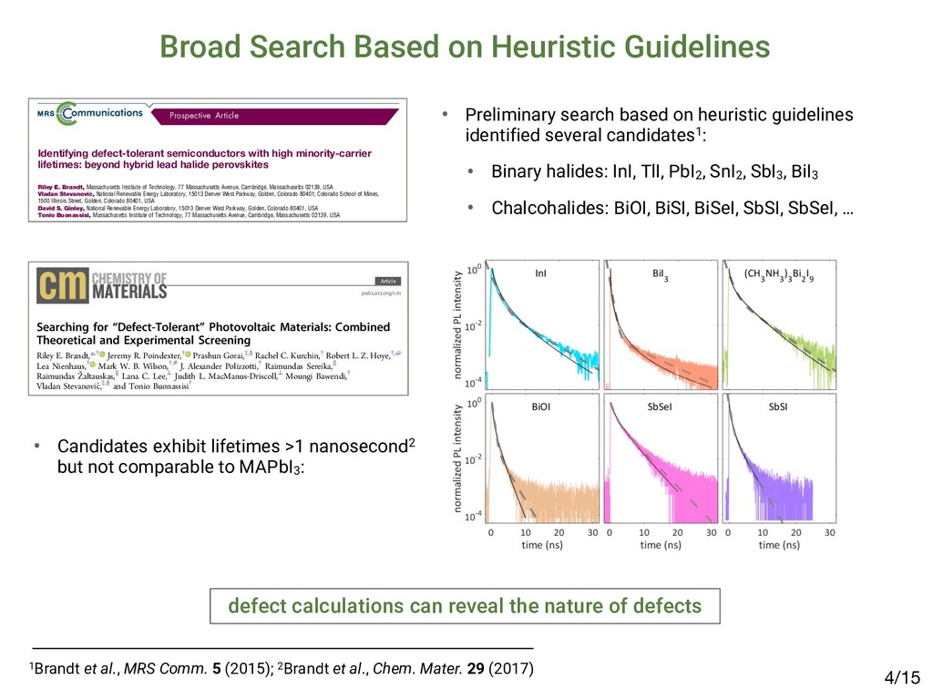
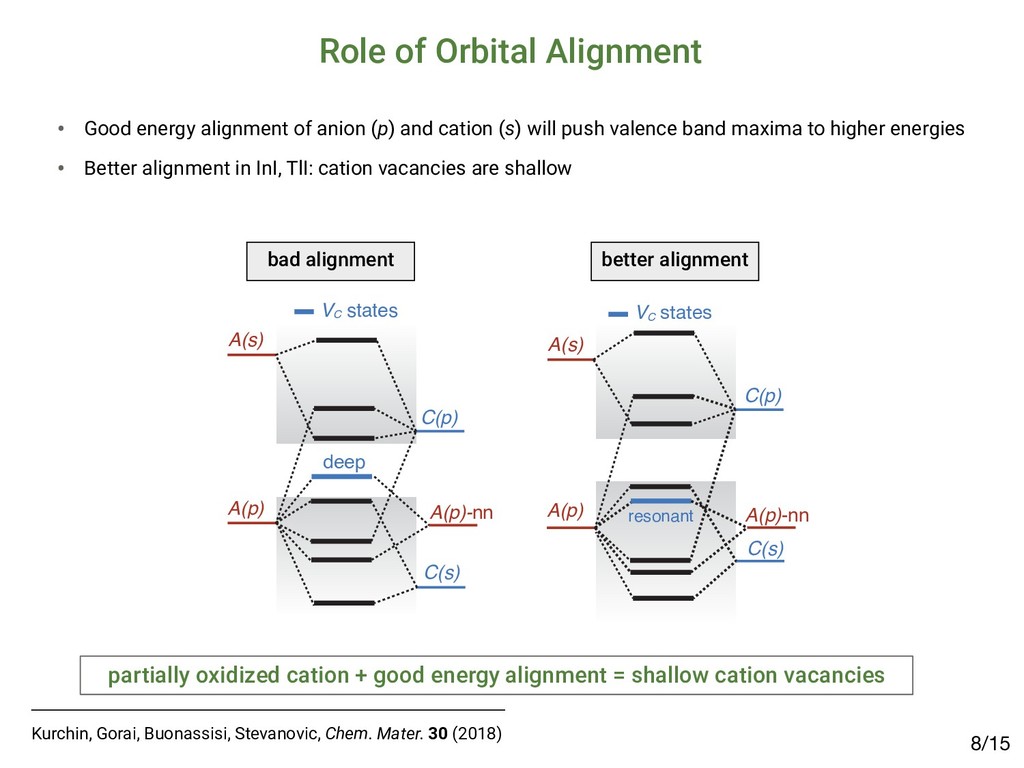
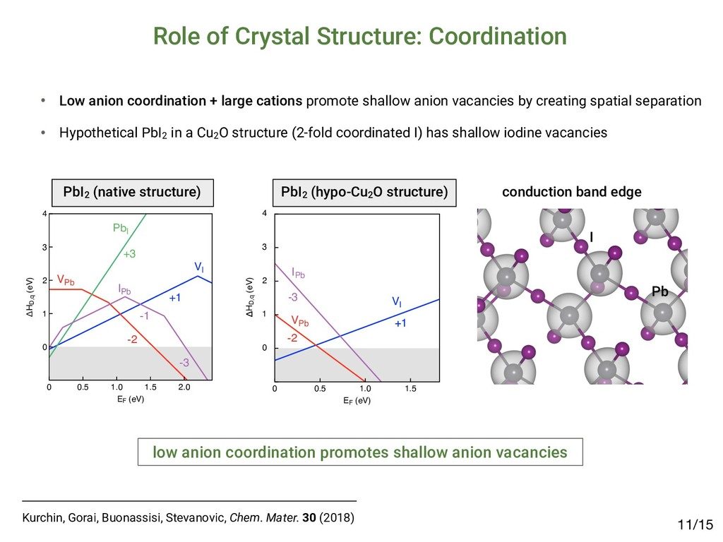
    on heuristic guidelines identified several candidates1: • Binary halides: InI, TlI, PbI2, SnI2, SbI3, BiI3 • Chalcohalides: BiOI, BiSI, BiSeI, SbSI, SbSeI, … Prospective Article Identifying defect-tolerant semiconductors with high minority-carrier lifetimes: beyond hybrid lead halide perovskites Riley E. Brandt, Massachusetts Institute of Technology, 77 Massachusetts Avenue, Cambridge, Massachusetts 02139, USA Vladan Stevanović, National Renewable Energy Laboratory, 15013 Denver West Parkway, Golden, Colorado 80401; Colorado School of Mines, 1500 Illinois Street, Golden, Colorado 80401, USA David S. Ginley, National Renewable Energy Laboratory, 15013 Denver West Parkway, Golden, Colorado 80401, USA Tonio Buonassisi, Massachusetts Institute of Technology, 77 Massachusetts Avenue, Cambridge, Massachusetts 02139, USA Address all correspondence to Riley E. Brandt, Tonio Buonassisi at [email protected]; 
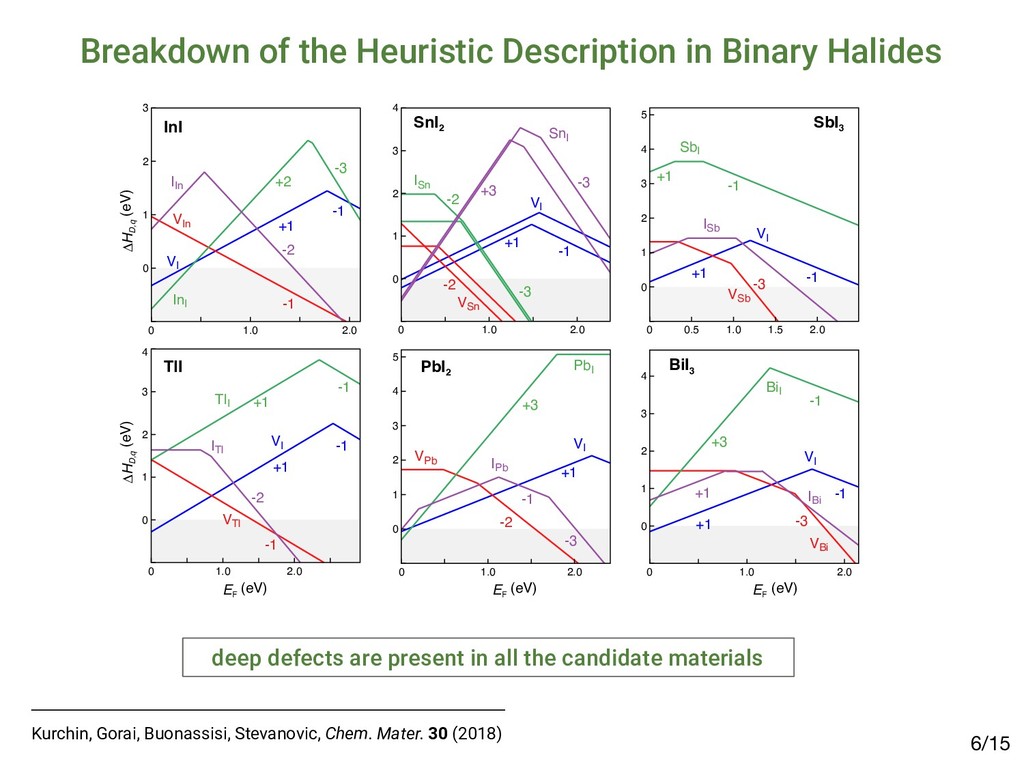
[email protected] (Received 27 March 2015; accepted 23 April 2015) Abstract The emergence of methyl-ammonium lead halide (MAPbX3 ) perovskites motivates the identification of unique properties giving rise to excep- tional bulk transport properties, and identifying future materials with similar properties. Here, we propose that this “defect tolerance” emerges from fundamental electronic-structure properties, including the orbital character of the conduction and valence band extrema, the charge- carrier effective masses, and the static dielectric constant. We use MaterialsProject.org searches and detailed electronic-structure calculations to demonstrate these properties in other materials than MAPbX3 . This framework of materials discovery may be applied more broadly, to accelerate discovery of new semiconductors based on emerging understanding of recent successes. Introduction Many semiconductors have been studied over the last century for their possible use in photovoltaics (PVs), light-emitting diodes (LEDs), computing devices, sensors, and detectors. Of these, only a select few have achieved sufficient optoelectronic perfor- mance to transition into industrial manufacturing, and their iden- tification and development have been slow and mostly empirical. Recently, high-throughput computation and a deeper under- standing of the physics-based requirements for high performance have created the potential for an accelerated identification of functional materials with manufacturing potential. For example, materials screening criteria have been proposed to better focus the search for novel candidate PV materials; they include the op- tical band-gap energy[1,2] and abruptness of absorption onset,[3,4] in addition to boundary conditions of elemental abundance,[5] and manufacturing cost.[6,7] However, many materials have met these criteria and yet have not achieved industrially relevant conversion efficiencies (in excess of 10–15%) due to low minority-carrier lifetimes or diffusion lengths, e.g., in the case of Cu2 ZnSn(S,Se)4 ,[8] SnS,[9] and others.[10] Meanwhile, PV de- vices have emerged based on methyl-ammonium lead iodide (MAPbI3 ) and closely related halides (herein referred to as MAPbX3 ). MAPbI3 is a semiconductor, which has demonstrated exceptional minority-carrier lifetimes of 280 ns (in the mixed iodide–chloride composition)[11] and diffusion lengths up to 175 μm,[12] comparable with the best single-crystal semiconduc- tors. This, in addition to meeting the criteria above, has resulted in a dramatic realization of PV conversion efficiencies up to 20.1%[13,14] in 2015, from <4% in 2009.[15] This paper examines whether the dramatic success of MAPbX3 in PVs can be used as a basis to expand design criteria to identify new potential high-performance optoelectronic ma- terials. One of the most compelling questions engendered by MAPbX3 as an optoelectronic material is the degree to which it is unique, and whether its success can lead to the identifica- tion of materials with improved stability and lower toxicity, yet similar high performance. Clearly, as in previous design criteria the high optical absorption coefficient is important, but also es- sential are the long carrier diffusion lengths observed in MAPbX3 , enabled by high minority-carrier lifetime (τ) and mo- bility (μ).[11,16,17] The importance of τ and μ for device perfor- mance has been established[18] for the most highly performing PV materials, including silicon,[19] cadmium telluride,[20,21] copper indium gallium diselenide,[22] and gallium arsenide.[23] Oddly, these more direct transport parameters, τ and μ, are not traditionally considered essential screening criteria for novel candidate PV materials. This may be partially a conse- quence of the difficulty in measuring and/or calculating these parameters. The direct measurement of minority carrier τ and μ requires ultrafast electronic or optical sensors to capture tran- sients,[24–27] or strong steady-state signals,[28,29] and must be performed with PV-device-relevant illumination conditions, electrical fields, and transport directions. Calculating τ and μ from first-principles is even more challenging, given the lack of well-established and high-throughput methods to directly calculate electron–phonon interactions and/or trap capture cross-sections. Although it is possible to obtain some informa- tion about carrier mobility from effective masses, and MRS Communications (2015), 5, 265–275 doi:10.1557/mrc.2015.26 MRS COMMUNICATIONS • VOLUME 5 • ISSUE 2 • www.mrs.org/mrc ▪265 1Brandt et al., MRS Comm. 5 (2015); 2Brandt et al., Chem. Mater. 29 (2017) Searching for “Defect-Tolerant” Photovoltaic Materials: Combined Theoretical and Experimental Screening Riley E. Brandt,*,† Jeremy R. Poindexter,† Prashun Gorai,‡,§ Rachel C. Kurchin,† Robert L. Z. Hoye,†,@ Lea Nienhaus,† Mark W. B. Wilson,†,# J. Alexander Polizzotti,† Raimundas Sereika,∥ Raimundas Žaltauskas,∥ Lana C. Lee,⊥ Judith L. MacManus-Driscoll,⊥ Moungi Bawendi,† Vladan Stevanović,‡,§ and Tonio Buonassisi† † Massachusetts Institute of Technology, Cambridge, Massachusetts 02139, United States ‡ Colorado School of Mines, Golden, Colorado 80401, United States §National Renewable Energy Laboratory, Golden, Colorado 80401, United States ∥Faculty of Science and Technology, Lithuanian University of Educational Sciences, Vilnius 08106, Lithuania ⊥Department of Materials Science and Metallurgy, University of Cambridge, Cambridge CB3 0FE, United Kingdom * S Supporting Information ABSTRACT: Recently, we and others have proposed screening criteria for “defect-tolerant” photovoltaic (PV) absorbers, identifying several classes of semiconducting compounds with electronic structures similar to those of hybrid lead−halide perovskites. In this work, we reflect on the accuracy and prospects of these new design criteria through a combined experimental and theoretical approach. We construct a model to extract photoluminescence lifetimes of six of these candidate PV absorbers, including four (InI, SbSI, SbSeI, and BiOI) for which time-resolved photoluminescence has not been previously reported. The lifetimes of all six candidate materials exceed 1 ns, a threshold for promising early stage PV device performance. However, there are variations between these materials, and none achieve lifetimes as high as those of the hybrid lead−halide perovskites, suggesting that the heuristics for defect-tolerant semiconductors are incomplete. We explore this through first- principles point defect calculations and Shockley−Read−Hall recombination models to describe the variation between the measured materials. In light of these insights, we discuss the evolution of screening criteria for defect tolerance and high-performance PV materials. ▪ INTRODUCTION Thin-film polycrystalline photovoltaic (PV) materials offer the potential for lower-capital intensity manufacturing relative to crystalline silicon PV, but only if they can achieve high PV conversion efficiencies in excess of 20%.1,2 Long minority- carrier lifetimes are necessary to achieve high efficiency, yet to date, there have been only a few classes of polycrystalline semiconductors that have demonstrated minority-carrier life- times in excess of 1 ns.3 Three classes of thin-film PV absorbers have achieved bulk lifetimes in excess of 100 ns, and they materials: it allows power conversion efficiencies on the order of 10% in materials with strong optical absorption and suggests the potential for further improvements.3 Including InP and other III−V materials, as well as the Cu2 ZnSn(S,Se)4 family of materials14 in addition to CIGS, CdTe, and LHPs, there are several additional classes of thin-film inorganic (or hybrid organic−inorganic) polycrystalline semiconductors that are known to exceed this 1 ns threshold. In prior work, we hypothesized that a promising path to achieving these long lifetimes is through defect-tolerant Article pubs.acs.org/cm • Candidates exhibit lifetimes >1 nanosecond2 but not comparable to MAPbI3: ▪ RESULTS Photoluminescence Lifetime. TRPL data for all six materials are plotted in Figure 1. There is a clear variation in the TRPL behavior across the materials tested, with (CH NH ) Bi I and InI demonstrating the slowest decay, however, all effective lifetimes as well as “slow” expo time constants exceed 1 ns. Defect Calculations. Figure 2 shows calculated formation enthalpies as a function of Fermi level for I Figure 1. TRPL decay curves of all six materials measured. Dashed gray lines represent biexponential fits to the data, while solid black lines using a numerical model incorporating both Shockley−Read−Hall and radiative recombination (see the Supporting Information for det estimated parameters). The fluence used was 20 nJ/cm2 for all traces except for those of (CH3 NH3 )3 Bi2 I9 (approximately 1 nJ/cm2) and S nJ/cm2). Data for (CH3 NH3 )3 Bi2 I9 were reproduced with permission from ref 33. Chemistry of Materials A defect calculations can reveal the nature of defects /15 4
  5. First-principles Calculation of Defect Levels ∆ HD,q Fermi energy (EF

    ) VBM CBM 0 Eg q=0 -2 shallow +1 acceptor donor deep acceptor donor • Supercell approach with finite size corrections and GW-corrected band edges1 H D,q = E D,q E host + X i n i µ i + qE F + E corr 1Lany and Zunger, Phys. Rev. B 78 (2008) /15 5
  6. Breakdown of the Heuristic Description in Binary Halides Kurchin, Gorai,

    Buonassisi, Stevanovic, Chem. Mater. 30 (2018) VI VIn InI IIn InI -1 +1 -1 +2 -3 -2 0 1 2 3 0 1.0 2.0 VI VTl TlI ITl TlI -1 +1 +1 -1 -2 -1 0 1 2 3 4 0 1.0 2.0 VI VSn ISn SnI -2 +1 -3 -2 -3 +3 -1 0 1 2 3 4 0 1.0 2.0 VI VPb PbI IPb -2 +1 +3 -3 -1 0 1 2 3 4 5 0 1.0 2.0 VI VBi BiI IBi -3 +1 -1 +1 +3 -1 0 1 2 3 4 0 1.0 2.0 SnI 2 PbI 2 BiI 3 EF (eV) EF (eV) EF (eV) ∆ HD,q (eV) ∆ HD,q (eV) VI VSb +1 -3 ISb SbI -1 +1 -1 0 1 2 3 4 5 0 0.5 1.0 1.5 2.0 SbI 3 deep defects are present in all the candidate materials /15 6
  7. Refined Understanding /15 7 • Existing guidelines are based on

    chemistry - does not account for interactions of dangling bonds or structural relaxation upon defect formation prior understanding refined understanding cation vacancy A(p) A(p)-nn VC states deep C(p) C(s) A(s) A(p) band gap C(p) C(s) A(s) VC states shallow orbital chemistry and structure likely play a role in defect tolerance Kurchin, Gorai, Buonassisi, Stevanovic, Chem. Mater. 30 (2018)
  8. Role of Orbital Alignment /15 8 A(p) C(p) C(s) A(p)-nn

    resonant VC states A(p) A(p)-nn VC states deep C(p) C(s) A(s) A(s) bad alignment better alignment • Good energy alignment of anion (p) and cation (s) will push valence band maxima to higher energies • Better alignment in InI, TlI: cation vacancies are shallow partially oxidized cation + good energy alignment = shallow cation vacancies Kurchin, Gorai, Buonassisi, Stevanovic, Chem. Mater. 30 (2018)
  9. Role of Crystal Structure: Symmetry /15 9 1Shi and Du,

    Phys. Rev. B 90 (2014); 2Kurchin, Gorai, Buonassisi, Stevanovic, Chem. Mater. 30 (2018) • Crystal site symmetry can promote shallow anion vacancies e.g. CsCl structure type1,2 TlBr: conduction band edge Tl Br • Anion vacancy is deep in rocksalt TlBr1 but shallow in CsCl structure VBr VTl TlBr BrTl -1 +1 +2 -2 HD,q (eV) 0 1 2 3 4 EF (eV) 0 1.0 2.0 3.0 TlBr (CsCl structure): I-rich TlBr (CsCl structure)
  10. Role of Crystal Structure: Symmetry /15 10 1Shi and Du,

    Phys. Rev. B 90 (2014); 2Kurchin, Gorai, Buonassisi, Stevanovic, Chem. Mater. 30 (2018) suitable crystal site symmetry promotes shallow anion vacancies • Crystal site symmetry can promote shallow anion vacancies e.g. CsCl structure type1,2 • Anion vacancy is deep in orthorhombic InI but shallow in CsCl structure InI (hypo-CsCl structure) VI VIn InI IIn -1 +1 +2 -2 ΔHD,q (eV) −1 0 1 2 3 4 EF (eV) 0 0.5 1.0 1.5 VI VIn InI IIn -1 +1 -1 ΔHD,q (eV) −1 0 1 2 3 4 EF (eV) 0 0.5 1.0 1.5 2.0 InI (orthorhombic)
  11. Role of Crystal Structure: Coordination /15 11 • Low anion

    coordination + large cations promote shallow anion vacancies by creating spatial separation • Hypothetical PbI2 in a Cu2O structure (2-fold coordinated I) has shallow iodine vacancies HD,q (eV) 0 1 2 3 4 VI VPb IPb -2 +1 -3 EF (eV) 0 0.5 1.0 1.5 PbI2 (hypo-Cu2O structure) conduction band edge I Pb low anion coordination promotes shallow anion vacancies Kurchin, Gorai, Buonassisi, Stevanovic, Chem. Mater. 30 (2018) VI VPb PbI IPb -2 +1 +3 -3 -1 ΔHD,q (eV) 0 1 2 3 4 EF (eV) 0 0.5 1.0 1.5 2.0 PbI2 (native structure)
  12. Tradeoffs and Other Features /15 12 • Chemical and structural

    features appear to operate independently • InI, TlI: ns2 cation, bad structure - shallow cation but deep anion vacancies • WO3: ns2 cation absent, good structure - deep cation vacancies but shallow anion vacancies VO WO OW VW WO3: O-rich +2 -2 -3 -6 -1 -3 W O ΔHD,q (eV) 0 2 4 6 8 EF (eV) 0 0.5 1.0 1.5 2.0 Kurchin, Gorai, Buonassisi, Stevanovic, Chem. Mater. 30 (2018) TlBr (225) TlBr (221) TlI (63) TlI (221) InI (63) InI (221) intolerant tolerant E - Evacuum (eV) −8 −6 −4 −2 0 • Absolute band edge positions: CB edge lower in defect-tolerant structures with shallow anion vacancies
  13. Defect-Tolerance in Ternary Semiconductors: MAPbI3 /15 13 • Pseudo-binary: No

    MA contribution to band edges 1Miyata et al., Nature Physics 11 (2015) • Heuristic guidelines: Partially-oxidized cation: Pb2+ Large dielectric constants: MA dipole contributes Low effective masses1: ~0.1 me • Refined guidelines: Orbital alignment sub-optimal: Pb(6s) and I(5p) but .. Desirable structure: low anion coordination Does MAPbI3 fair well within these refined guidelines? VB CB MAPbI3 I(5p) Pb(6p) E g Pb(6s) ternary and multinary semiconductors offer more tunability to satisfy these criteria
  14. Extending the Refined Guidelines to Ternary Semiconductors /15 14 refined

    guidelines need to be further refined! PbTlI3 Pb Tl I • Preliminary search based on presence of ns2 cation and low anion coordination VI VTl PbTlI3 : I-rich VPb ΔHD,q (eV) −1 0 1 2 3 EF (eV) 0 1 2 • PbTlI3: anion is 3-fold coordinated • Iodine vacancies: states ~200 meV from band edges but low concentrations • Conduction band: not just p states of ns2 cation - also I(p) states
  15. Outlook Funding and Computational Resources National Science Foundation - SusChem

    DOE Energy Frontier Research Center CNGMD NREL High Performance Computing (HPC) • A refined understanding of the chemical and structural features for defect tolerance • Shallow cation vacancies: partially-oxidized cation + good energy alignment • Shallow anion vacancies: suitable crystal site symmetry or low anion coordination • Additional factors for defect tolerance to interstitials • Extension of guidelines to ternary chemistries needs careful consideration