Upgrade to Pro — share decks privately, control downloads, hide ads and more …

SPIE 2012 Amsterdam Talk: Silicon Immersion Gratings

gully
July 06, 2012

SPIE 2012 Amsterdam Talk: Silicon Immersion Gratings

This deck is my invited talk at the SPIE Astronomical Telescopes and Instrumentation conference in Amsterdam. The talk describes the immersion grating for IGRINS, and all the process steps and metrology that went into it.

gully

July 06, 2012
Tweet

More Decks by gully

Other Decks in Science

Transcript

  1. Paper # 8450-99 Near infrared metrology of high performance silicon

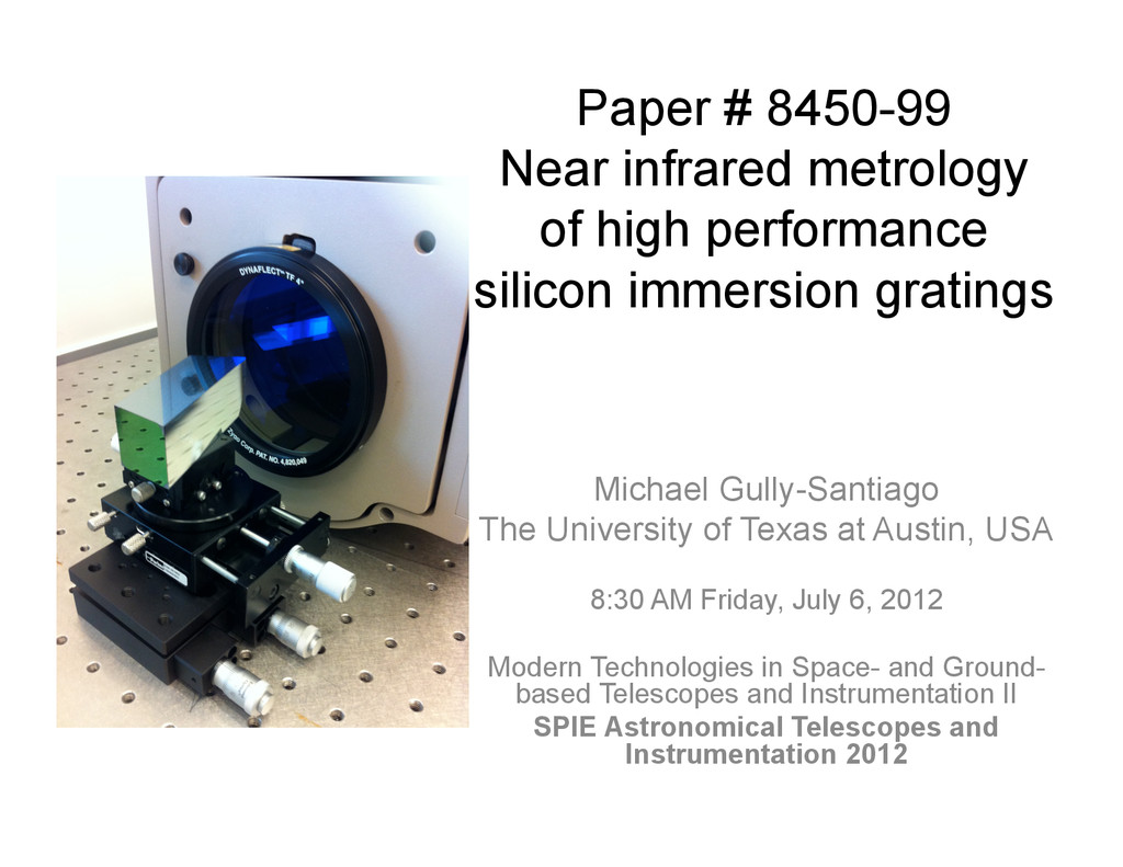
    immersion gratings Michael Gully-Santiago The University of Texas at Austin, USA 8:30 AM Friday, July 6, 2012 Modern Technologies in Space- and Ground- based Telescopes and Instrumentation II SPIE Astronomical Telescopes and Instrumentation 2012
  2. Past •  Diffraction gratings •  Immersion grating history •  Grating

    production at UT Austin •  Fabrication and process Present •  IGRINS Immersion grating: CA1a •  Metrology: –  interferometry –  spectral purity –  efficiency Future •  Direct writing: Electron beam lithography -0.15 0.00 0.15 -0.15 0.00 0.15 -0.05 0.00 0.05 Marsh,  Mar,  &  Jaffe  2007  
  3. Normal blazed reflection grating Diffraction Gratings & Applications Loewen and

    Popov 1997 β   α   Air   n≈1.0   Metal   € mλ = σ(sinα + sinβ) σ   gra0ng   normal   λ  
  4. Immersion grating Diffraction Gratings & Applications Loewen and Popov 1997

    β`   α`   Si   n≈3.4   Metal   σ   gra0ng   normal   λ/n € m λ n = σ(sin ʹ′ α + sin ʹ′ β )
  5. Spectral resolution in immersion •  R = λ/δλ •  R

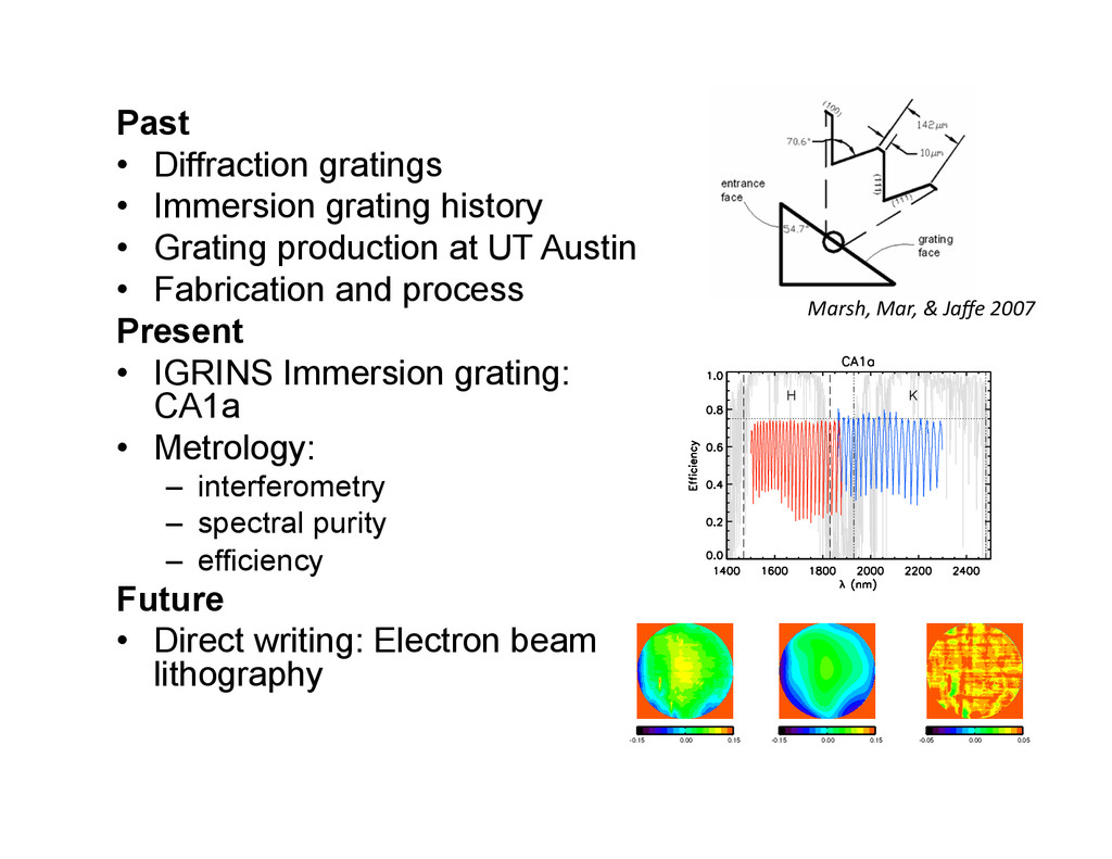
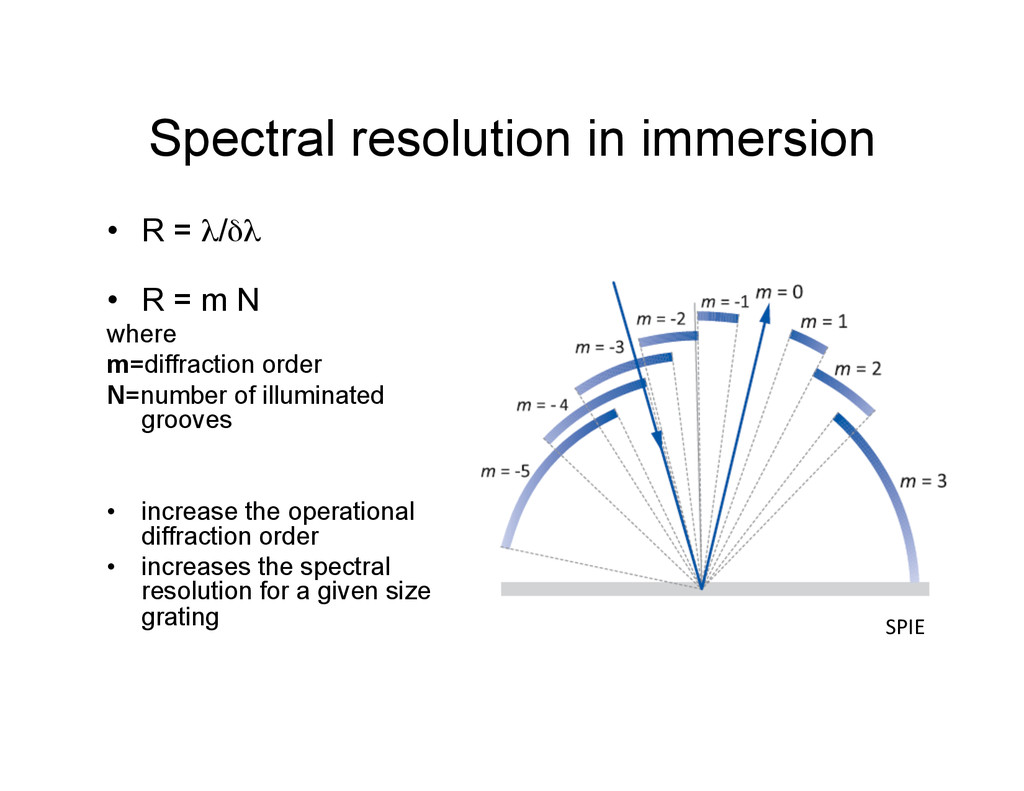
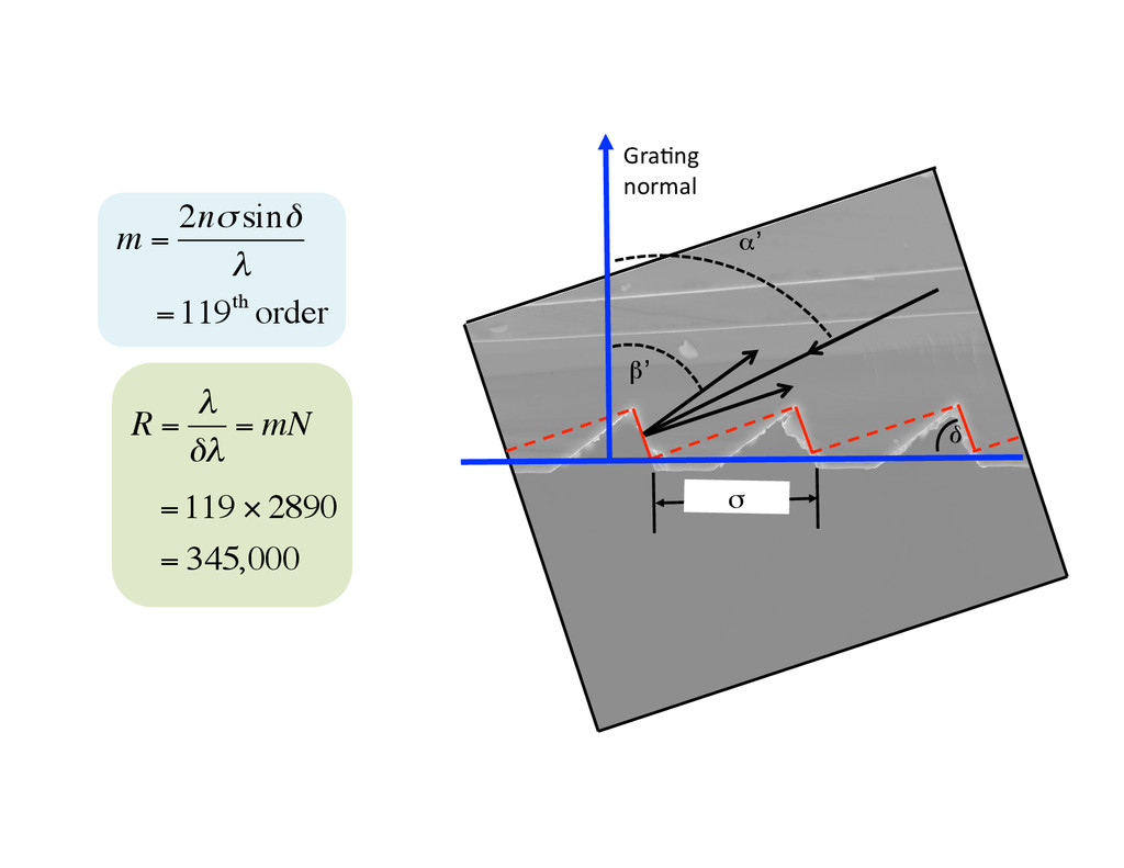
    = m N where m=diffraction order N=number of illuminated grooves •  increase the operational diffraction order •  increases the spectral resolution for a given size grating SPIE  
  6. Immersion gratings are not new Fraunhofer 1787 – 1826 first

    noted the effect of increased spectral resolution by immersing gratings in liquids of high refractive index Huelthén and Neuhaus, Nature, 1954
  7. Heritage Si gratings from UTexas group Grisms: SOFIA FORCAST SPIE:

    Deen et al. 2008 JWST NIRCAM SPIE: Jaffe et al 2008, Gully-Santiago et al. 2010 Immersion gratings: Marsh, Mar, & Jaffe 2007
  8. IGRINS,  the  Immersion  Gra0ng  Infrared  Spectrometer     University of

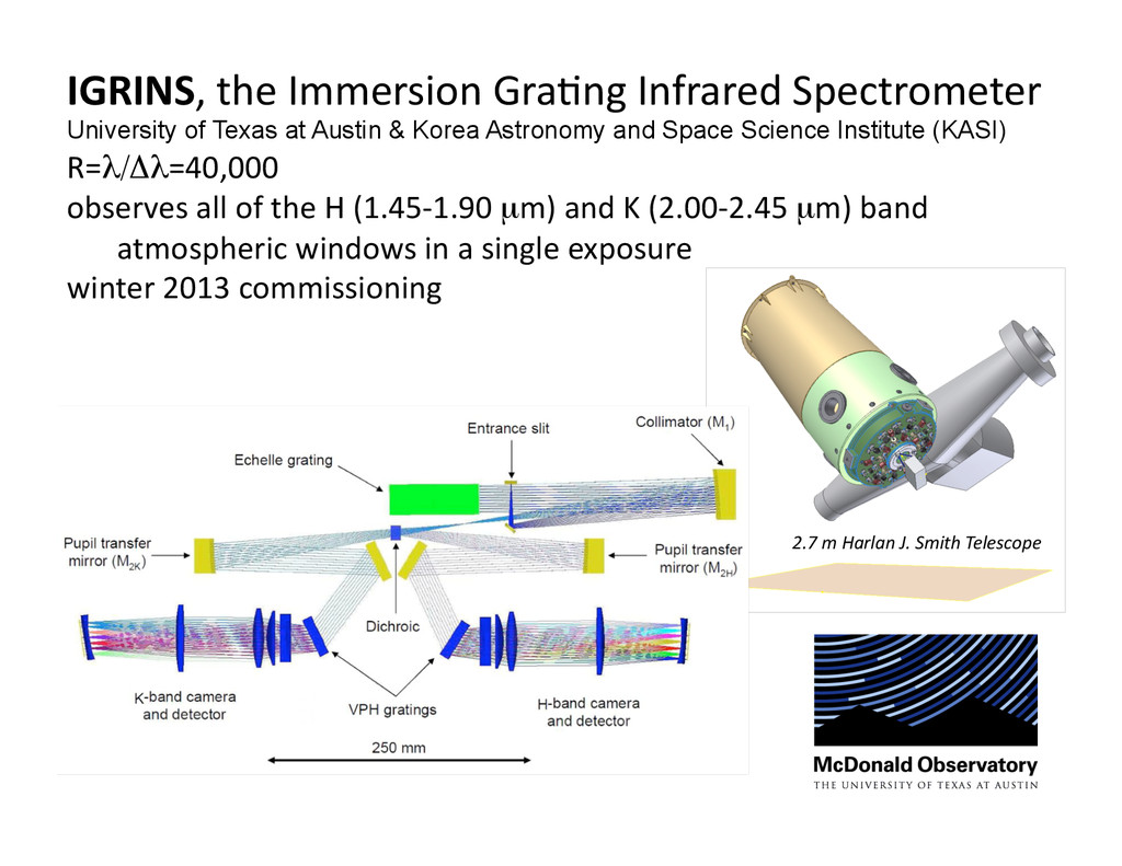
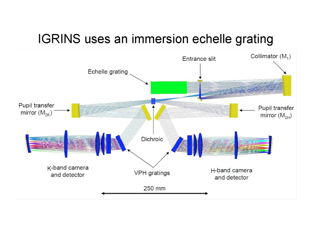
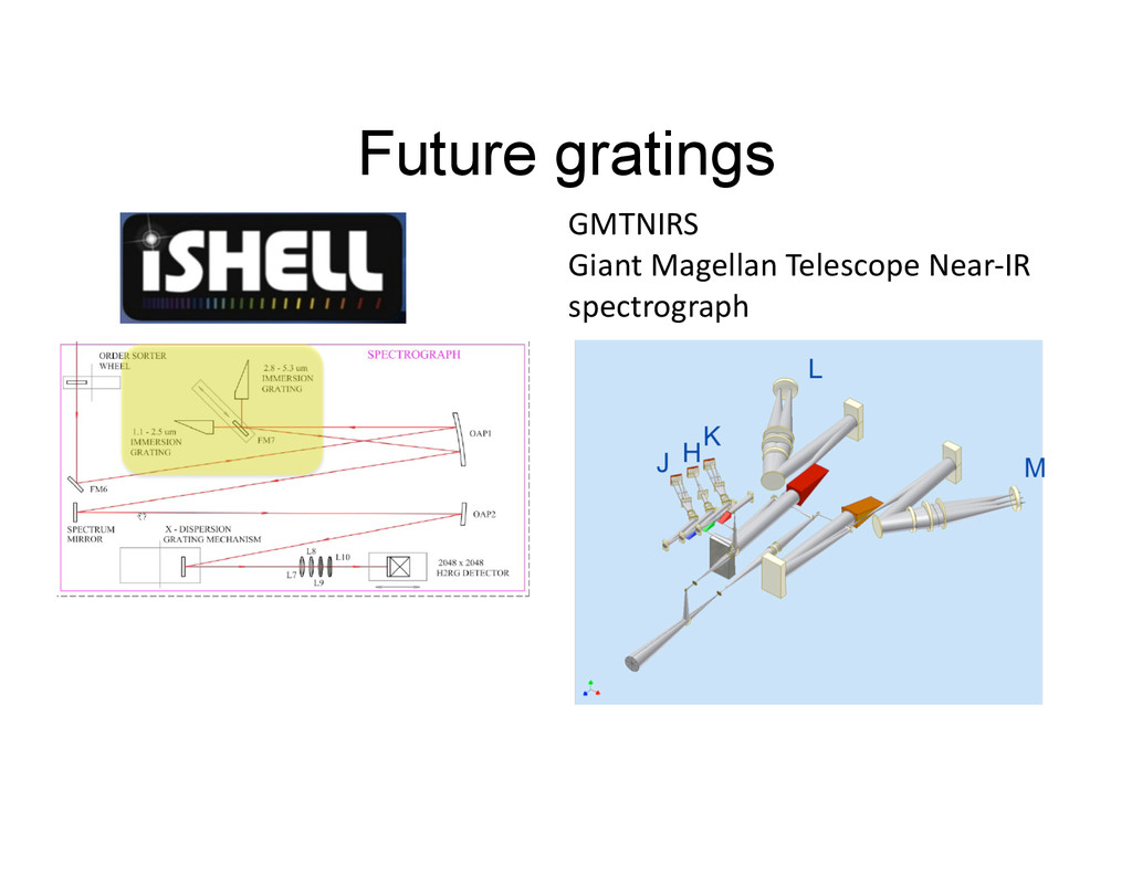
    Texas at Austin & Korea Astronomy and Space Science Institute (KASI) R=λ/Δλ=40,000   observes  all  of  the  H  (1.45-­‐1.90  µm)  and  K  (2.00-­‐2.45  µm)  band    atmospheric  windows  in  a  single  exposure   winter  2013  commissioning   2.7  m  Harlan  J.  Smith  Telescope  
  9. Silicon crystal properties Monolithic  crystalline  Si  ingot     Scanning

     electron  micrographs   (SEM)  of  Si  crystal  planes:     Top:  conven0on  Si  wafer   BoTom:  Bias  cut  Si  wafer  
  10. CA1 We cut two immersion gratings from this parent substrate.

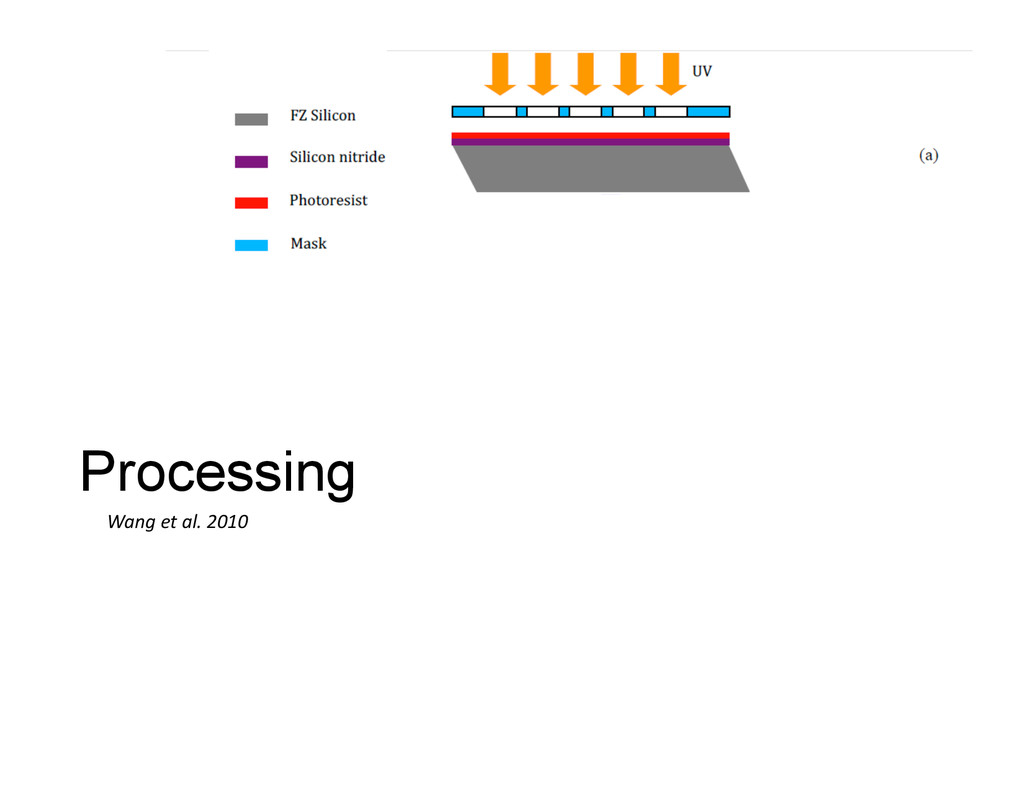
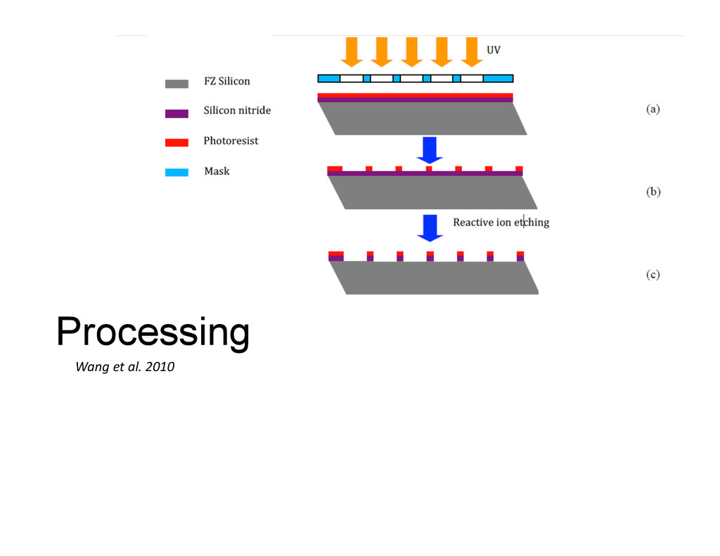
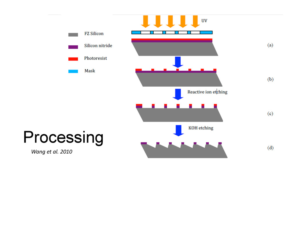
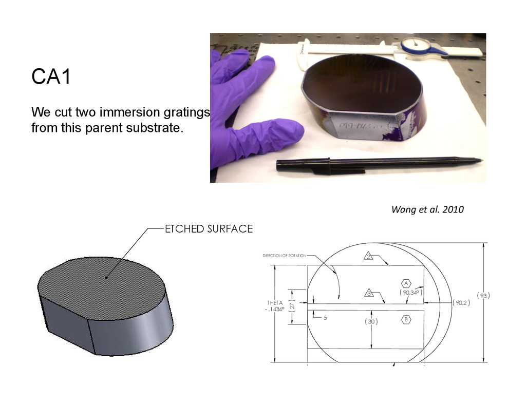
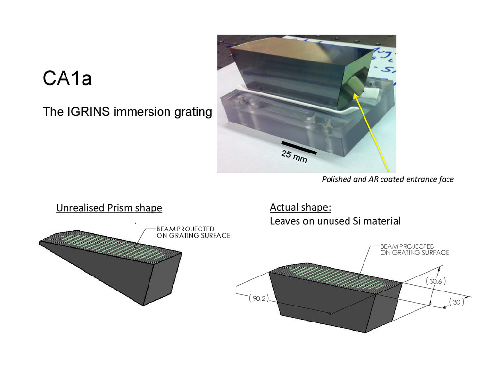
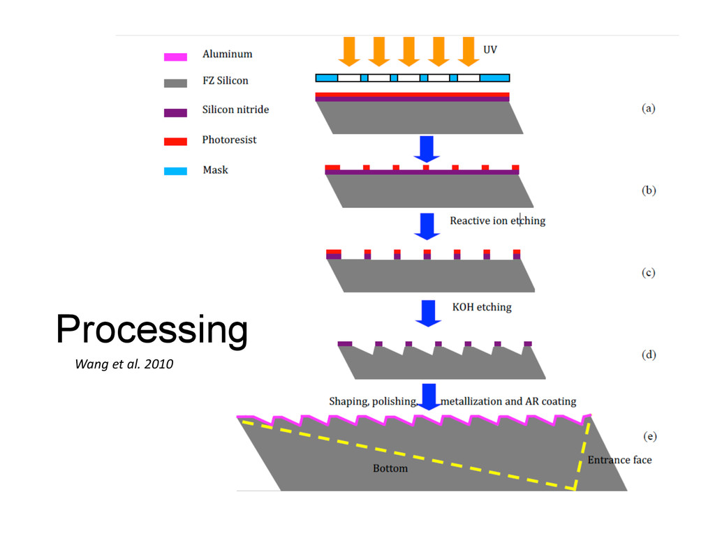
    30 5 - .1434° THETA ETCHED SURFACE 1 3 27 PARENT SUBSTRATE AS PROVIDED TO VENDOR ETCHED PROFILE LAYOUT 53.5 Wang  et  al.  2010   90.2 30 5 - .1434° THETA 90.34° 103 71.66° B C D 8 7 6 5 4 3 2 NOTES: 1. VENDOR WILL GRIND FACE 2 0.1434 DEGREES (THETA) CW TO FACE 1 2. VENDOR WILL SAW PIECE A FROM PIECE B . CUT WILL FALL WITHIN 5mm KERF SHOWN IN SKETCH 3. FACE 3 SHOULD THEN BE GROUND PARALLEL TO FACE 2 4. FACE 4 SHOULD THEN BE GROUND AT 71.66 and 89.68 DEGREE COMPOUND ANGLE TO ETCHED GRATING SURFACE (SEE SHEET 1) NOTES CONT'D: 5. PROCESS REPEATS FOR PIECE B 6. PIECE B TO BE CUT AT SAME SETUP AS A 7. CONTACT DR. WEISONG WANG AT 512-471-0886 OR DR. DAN JAFFE AT 51 WITH ANY QUESTIONS ETCHED SURFACE 1 3 2 A B DIRECTION OF ROTATION 27 93 ETCHED SURFACE 4 53.5 100
  11. 25 mm CA1a The IGRINS immersion grating 13 CE 1

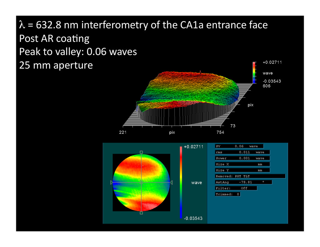
    B 71.66°±.025° A WHERE INDICATED 4 CORNER EFFECT DUE TO SHAPE OF PARENT MATERIAL FOR PROCESS USING 1200 GRIT WHEEL .25mm BEVEL EXCEPT 6. CONTACT DR. WEISONG WANG AT 512-471-0886 OR DR. DAN JAFFE AT 512-471-3425 WITH ANY QUESTIONS 5 NOTE: TNESS 1/4 WAVE AT 632.8nm OVER RT OF 90% OCESS D C 6 5 4 3 2 1 BEAM PROJECTED ON GRATING SURFACE 30.6 30 90.2 4 BEAM PROJECTED ON ENTRANCE SURFACE ETCHED LINES PERPENDICULAR TO DATUM A TO PROFILE ON SHEET 2 ) ANGLE SHOWN ONLY TO ORIENT VIEWER 90.34° ( 90.2 D C B 3 2 1 BEAM PROJECTED ON GRATING SURFACE OF PARENT MATERIAL 30.429 29 2.5 88.95 30.5 84.502 DETAIL B SCALE 4 : 1 30.429 30.482 ACE Unrealised  Prism  shape   Actual  shape:   Leaves  on  unused  Si  material   Polished  and  AR  coated  entrance  face  
  12. Gra0ng   normal   δ αʼ# βʼ σ m =

    2nσ sinδ λ =119th order € R = λ δλ = mN € =119 × 2890 = 345,000
  13. 2.4 Å 16.6Å 24.2 Å Measured  surface  roughness  of  a

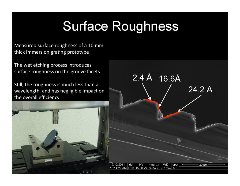
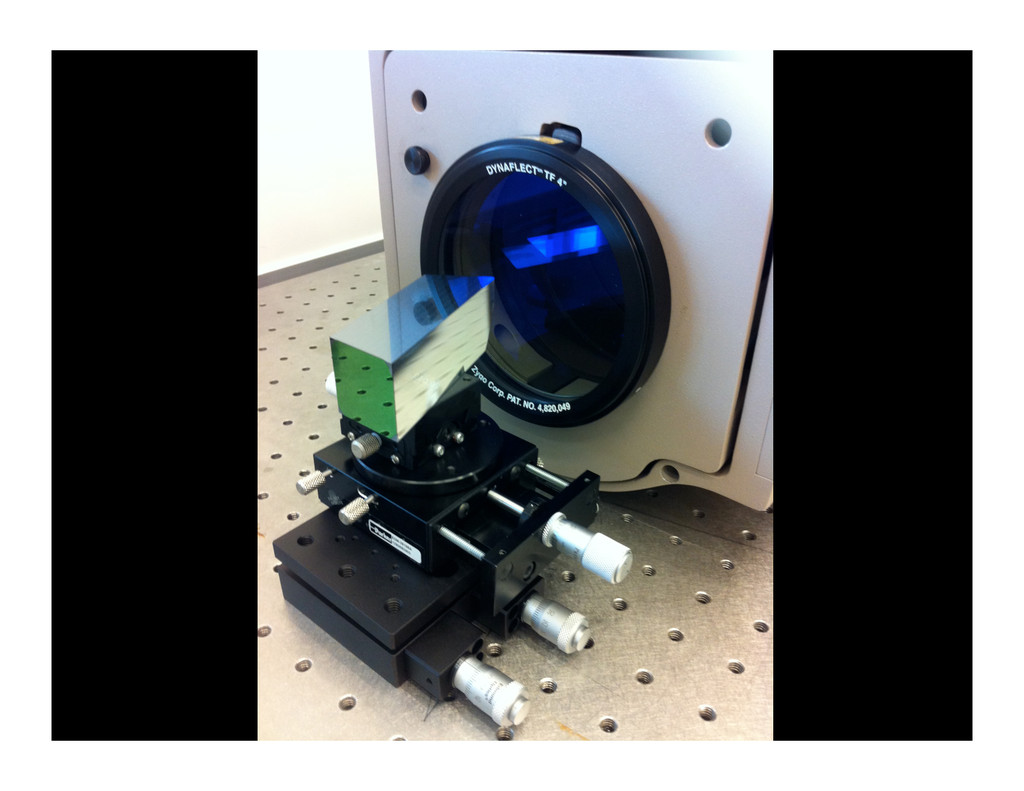
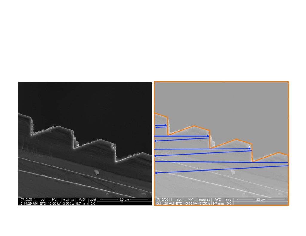
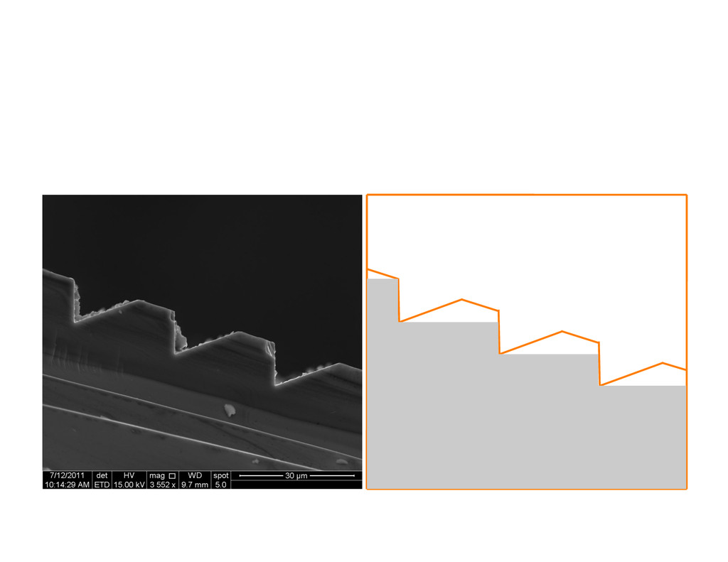
     10  mm   thick  immersion  gra0ng  prototype   The  wet  etching  process  introduces   surface  roughness  on  the  groove  facets   S0ll,  the  roughness  is  much  less  than  a   wavelength,  and  has  negligible  impact  on   the  overall  efficiency   Surface Roughness
  14. 632 nm in air is comparable to ~2.2 µm in

    immersion 25 mm beam is projected over ~80 mm across the hypotenuse of the R3 echelle Marsh,  Mar,  and  Jaffe  2007   Optical interferometry
  15. λ  =  632.8  nm  interferometry  of  the  CA1a  entrance  face

      Post  AR  coa0ng     Peak  to  valley:  0.06  waves   25  mm  aperture  
  16. λ   =  632.8  nm  interferometry  of  the  CA1a  R3  facets

        Post  aluminiza0on   Peak  to  valley:  0.17  waves   25  mm  aperture  
  17. -20 -10 0 10 20 x (FWHMs) 10-6 10-5 10-4

    10-3 10-2 10-1 100 Normalized Flux -20 -10 0 10 20 x (FWHMs) -20 -10 0 10 20 y (FWHMs) Spectral purity PSF at l = 632.8 nm from 25 mm beam interferogram
  18. -20 -10 0 10 20 x (!632 /D 25 )

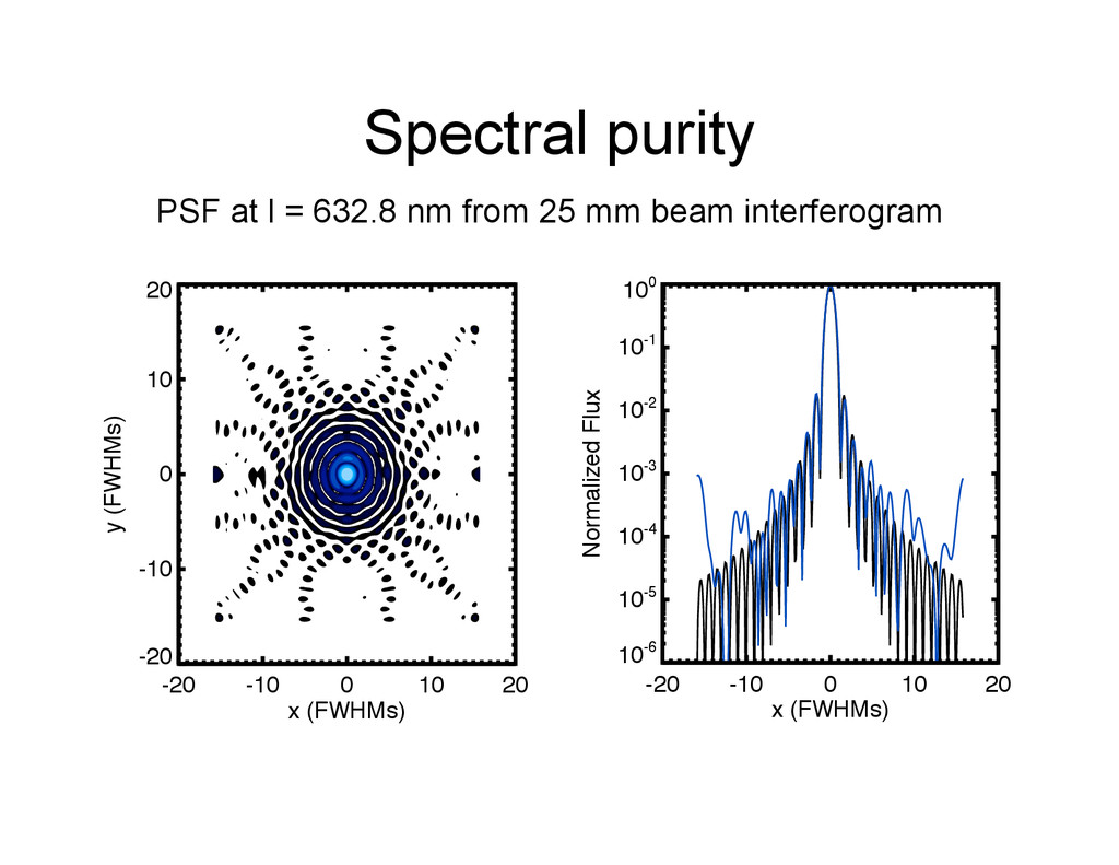
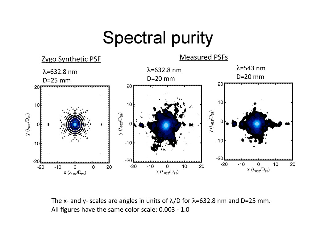
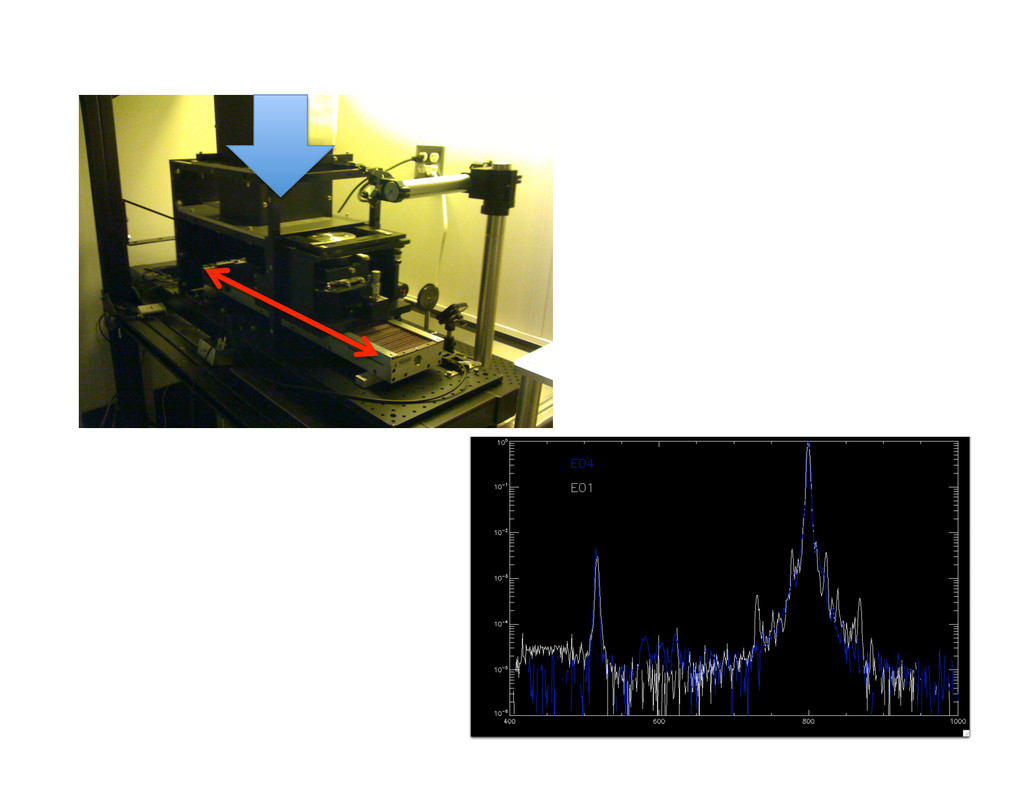
    -20 -10 0 10 20 y (!632 /D 25 ) -20 -10 0 10 20 x (!632 /D 25 ) -20 -10 0 10 20 y (!632 /D 25 ) -20 -10 0 10 20 x (!632 /D 25 ) -20 -10 0 10 20 y (!632 /D 25 ) The  x-­‐  and  y-­‐  scales  are  angles  in  units  of  λ/D  for  λ=632.8  nm  and  D=25  mm.       All  figures  have  the  same  color  scale:  0.003  -­‐  1.0     λ=632.8  nm     D=25  mm   λ=543  nm     D=20  mm   λ=632.8  nm     D=20  mm   Measured  PSFs   Zygo  Synthe0c  PSF   Spectral purity
  19. -20 -10 0 10 20 x (!632 /D 25 )

    10-6 10-5 10-4 10-3 10-2 10-1 100 Normalized Flux Model Measured λ (nm)   Ig /Il Ig /Il Meas./Model Green 543.5 0.0012 0.0016 1.30 Zygo (red) 632.8 0.0009 0.0009 1.00 Meas. (red) 632.8 0.0009 0.0011 1.22 IR 1523 0.0018 <0.0120 <6.52 Marsh,  Mar,  &  Jaffe  2007   Amplitude:  A  =  3.2  nm   Period:  P=1.6  mm   -50 0 50 x (!632 /D 25 ) 10-6 10-5 10-4 10-3 10-2 10-1 100 Normalized Flux Ghost amplitude
  20. Custom robotic grating efficiency test apparatus *1.45 < λ (µm)

    < 2.3 *δλ ~ 1.0 nm *D ~ 10 mm *Al ref. mirror *unpolarized
  21. *Efficiency relative to Al mirror *Slightly different incidence angles, α,

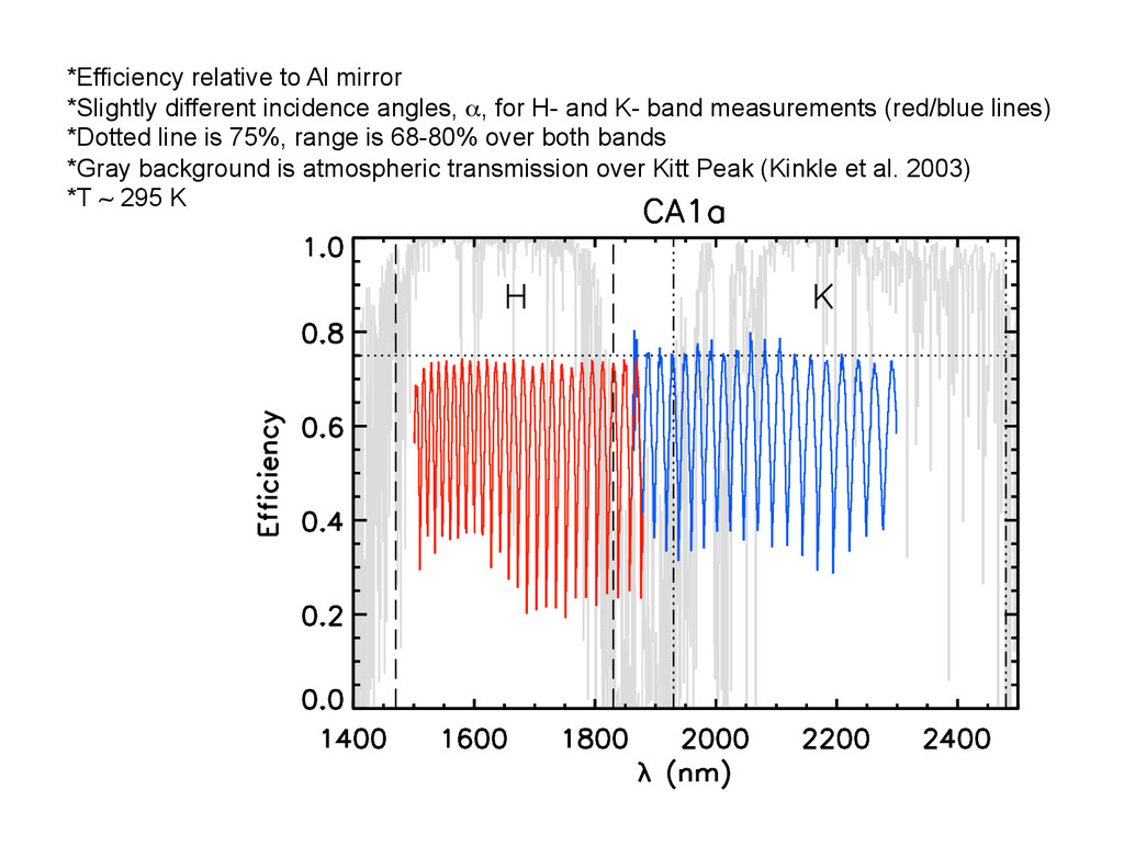
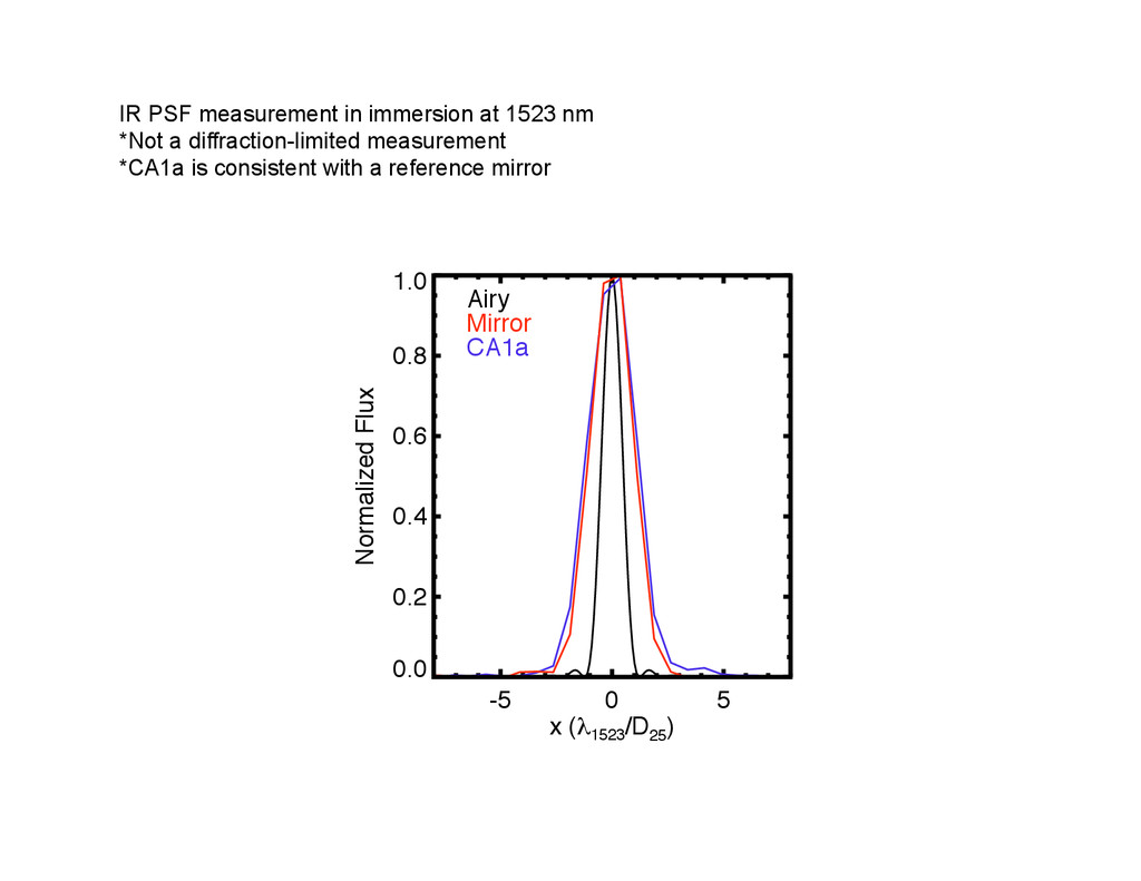
    for H- and K- band measurements (red/blue lines) *Dotted line is 75%, range is 68-80% over both bands *Gray background is atmospheric transmission over Kitt Peak (Kinkle et al. 2003) *T ~ 295 K
  22. *Black dots show the observed blaze peaks. …as refractive index

    changes the wavelengths that were once on-blaze are now off- blaze. Temperature-­‐dependent  refracGve  index  of  silicon…   Frey,  Leviton,  &  Madison  2006  
  23. Metrology Summary •  Facet surface roughness is ~16 Å – 

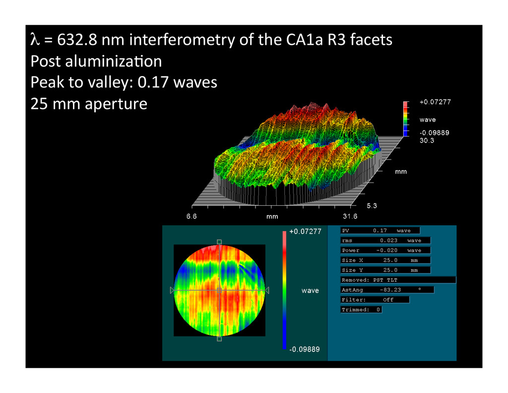
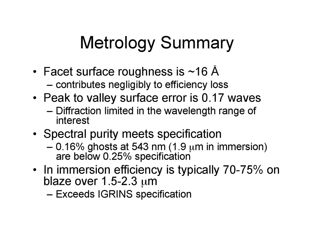
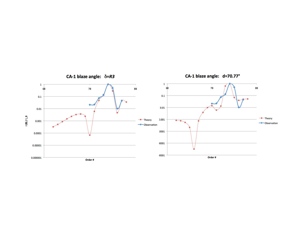
    contributes negligibly to efficiency loss •  Peak to valley surface error is 0.17 waves –  Diffraction limited in the wavelength range of interest •  Spectral purity meets specification –  0.16% ghosts at 543 nm (1.9 µm in immersion) are below 0.25% specification •  In immersion efficiency is typically 70-75% on blaze over 1.5-2.3 µm –  Exceeds IGRINS specification
  24. Future work preview: better and bigger gratings •  Better: – 

    reduce repetitive error amplitude –  reduce large scale surface error •  Bigger: –  Currently limited to 100 mm diameter substrate –  Next generation instruments (GMTNIRS?) will require 150 mm, or up to 200 mm boules Contact lithography will not work for larger gratings
  25. Direct writing experiments: electron beam lithography (JPL) & UV nanoruler

    (MIT) •  NASA JPL Microdevices Lab (MDL) – JEOL 9300-FS •  Non-flat surfaces •  Large Computer generated holograms •  Grayscale lithography Historical challenge has been periodic errors introduced from e-beam field stitching errors
  26. -0.30 0.00 0.30 -0.30 0.00 0.30 -0.10 0.00 0.10 -0.30

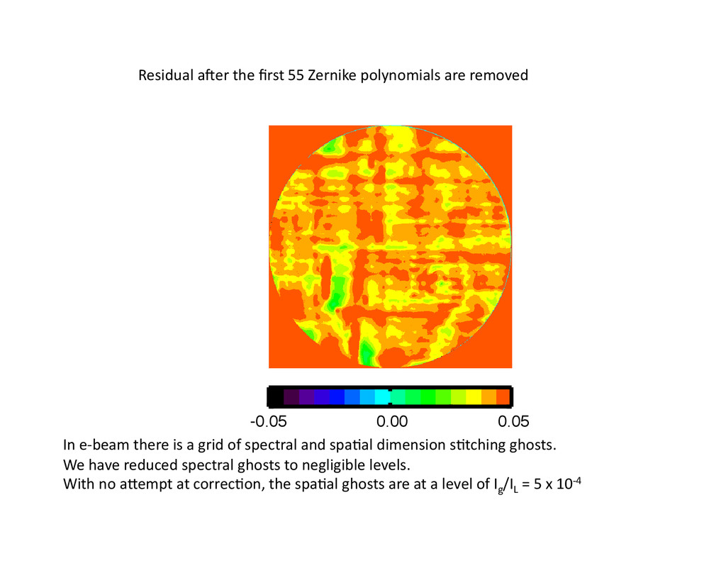
    0.00 0.30 -0.30 0.00 0.30 -0.10 0.00 0.10 E-beam direct writing initial results First  prototype  immersion   gra0ng   Second  immersion   gra0ng,  improved  wri0ng   strategy   10  mm  thick  R3  clones  of  the  IGRINS  surface,  directly  wriSen  with  the  JEOL  9300FS   25  mm  beam  interferograms  on  the  same  color  scale,  in  waves  of  632  nm  surface  deviaGon   Measured   55  term  Zernike  fit   Residual  
  27. Other future projects 1) Bonded Grisms 2) Cryogenic VPH gratings

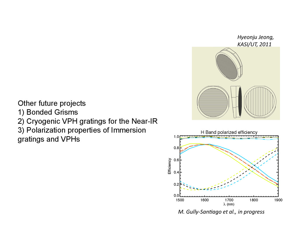
    for the Near-IR 3) Polarization properties of Immersion gratings and VPHs H Band polarized efficiency 1500 1600 1700 1800 1900 h (nm) 0.0 0.2 0.4 0.6 0.8 1.0 Efficiency Hyeonju  Jeong,   KASI/UT,  2011   M.  Gully-­‐SanGago  et  al.,  in  progress  
  28. Thank you NASA Graduate Student Researchers Program NSF ATI Grant

    AST-0705064 NASA APRA Grant NNX10AC68G UT Austin Dan Jaffe Weisong Wang Cindy Brooks Casey Deen (now at MPIA Heidelberg) JPL MDL Dan Wilson Rich Muller
  29. Immersion grating Diffraction Gratings & Applications Loewen and Popov 1997

    Si   n≈3.4   Metal   σ   gra0ng   normal   λ/n € m λ n = σ(sin ʹ′ α + sin ʹ′ β )
  30. Immersion grating Diffraction Gratings & Applications Loewen and Popov 1997

    Si   n≈3.4   Metal   σ   gra0ng   normal   λ/n € m λ n = σ(sin ʹ′ α + sin ʹ′ β )
  31. Immersion grating Diffraction Gratings & Applications Loewen and Popov 1997

    Si   n≈3.4   λ/n € m λ n = σ(sin ʹ′ α + sin ʹ′ β ) λ   Air   n≈1.0  
  32. In  e-­‐beam  there  is  a  grid  of  spectral  and  spa0al

     dimension  s0tching  ghosts.   We  have  reduced  spectral  ghosts  to  negligible  levels.   With  no  aTempt  at  correc0on,  the  spa0al  ghosts  are  at  a  level  of  Ig /IL  =  5  x  10-­‐4   0.00 0.15 -0.05 0.00 0.05 Residual  ager  the  first  55  Zernike  polynomials  are  removed  
  33. Theory: CA1, !="=71.57, n Si =n(#), T=295K -30 -20 -10

    0 10 20 30 $ (deg) 0.0 0.2 0.4 0.6 0.8 1.0 1.2 Relative flux # = 1500.0 nm # = 1510.0 nm 118 119 120 121 122 Theory: CA1, !="=71.57, n Si =n(#), T=295K -30 -20 -10 0 10 20 30 $ (deg) 0.0 0.2 0.4 0.6 0.8 1.0 1.2 Relative flux # = 2300.0 nm # = 2325.0 nm 76 77 78 79 Predicted  efficiency  spectra  in  immersion,  normalized  to  the  blaze  peak.   The  diffracGon  and  refracGon  angles    depend  sensiGvely  on  the  refracGve     index  of  Silicon.  
  34. IR PSF measurement in immersion at 1523 nm *Not a

    diffraction-limited measurement *CA1a is consistent with a reference mirror -5 0 5 x (!1523 /D 25 ) 0.0 0.2 0.4 0.6 0.8 1.0 Normalized Flux Airy Mirror CA1a
  35. Gra0ng   normal   δ αʼ# βʼ σ mλ n

    = σ(sin ʹ′ α + sin ʹ′ β ) ʹ′ α ≈ ʹ′ β ≈ δ LiSrow  autocollimaGon:   GraGng  equaGon:   m = 2nσ sinδ λ = 2 × 3.44 × 27.36 × 0.95 1.5 =119th order € R = λ δλ = mN N = W σ = 25mm 27.36µm = 914 grooves =119 × 914 =109,000 cf.  Loewen  &  Popov  
  36. Orien0ng,  cujng,     polishing,  nitriding   2006-­‐  2008  

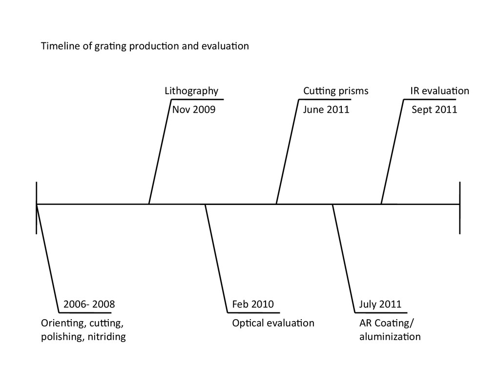
    Lithography   Nov  2009   July  2011   AR  Coa0ng/   aluminiza0on   June  2011   Cujng  prisms   Feb  2010   Op0cal  evalua0on   IR  evalua0on   Sept  2011   Timeline  of  gra0ng  produc0on  and  evalua0on  
  37. Periodic  errors  originate  in  the  UV   photolithography  process,  specifically

      the  transla0on  stage  motor  drive   Since  CA1,  we  have  reduced  the   periodic  errors  aTributable  to  the   motor  drive  to  negligible  levels    
  38. *The angle q is relative to the optical axis *The

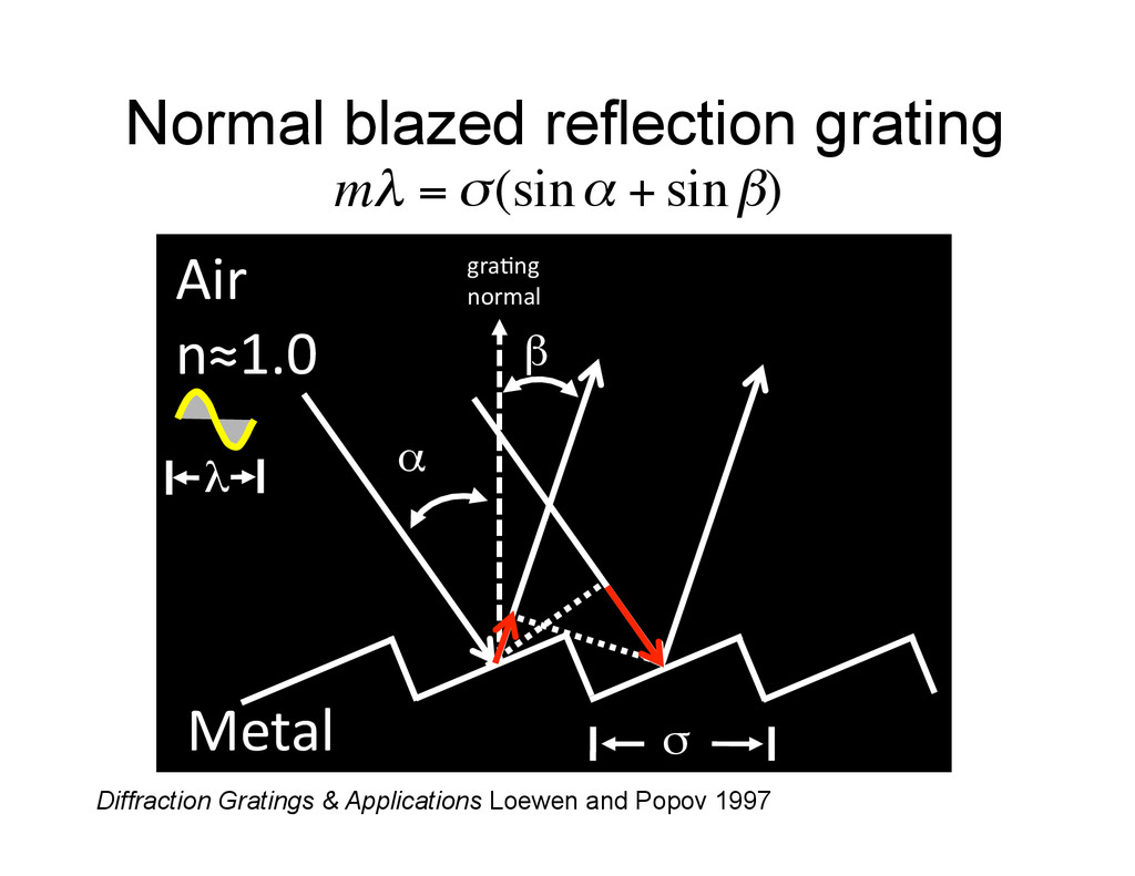
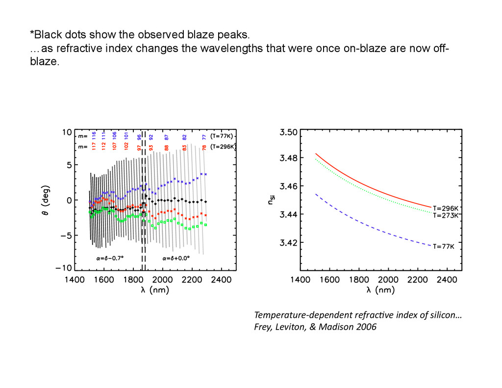
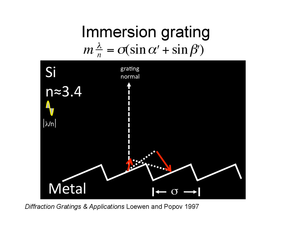
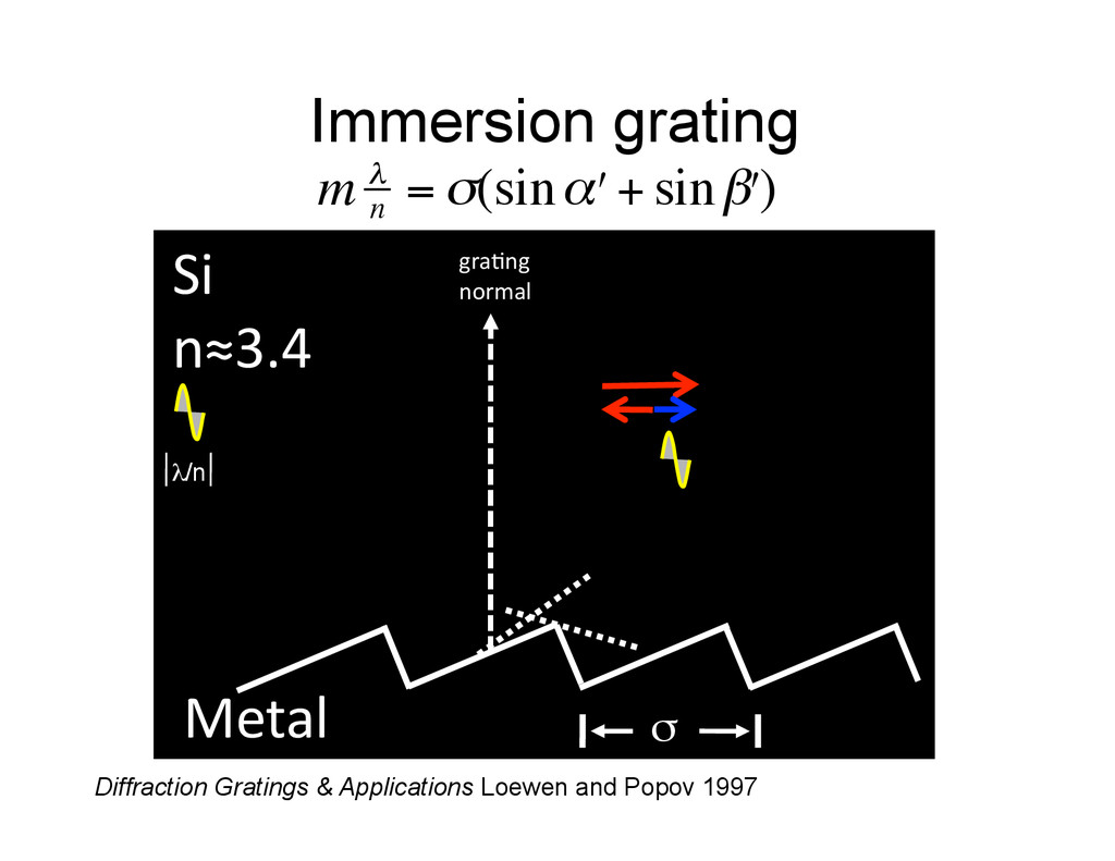
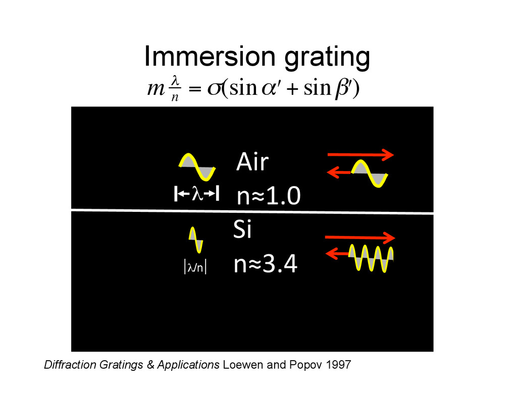
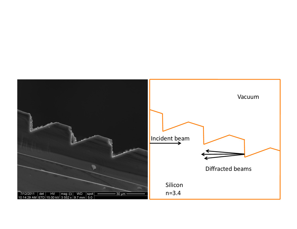
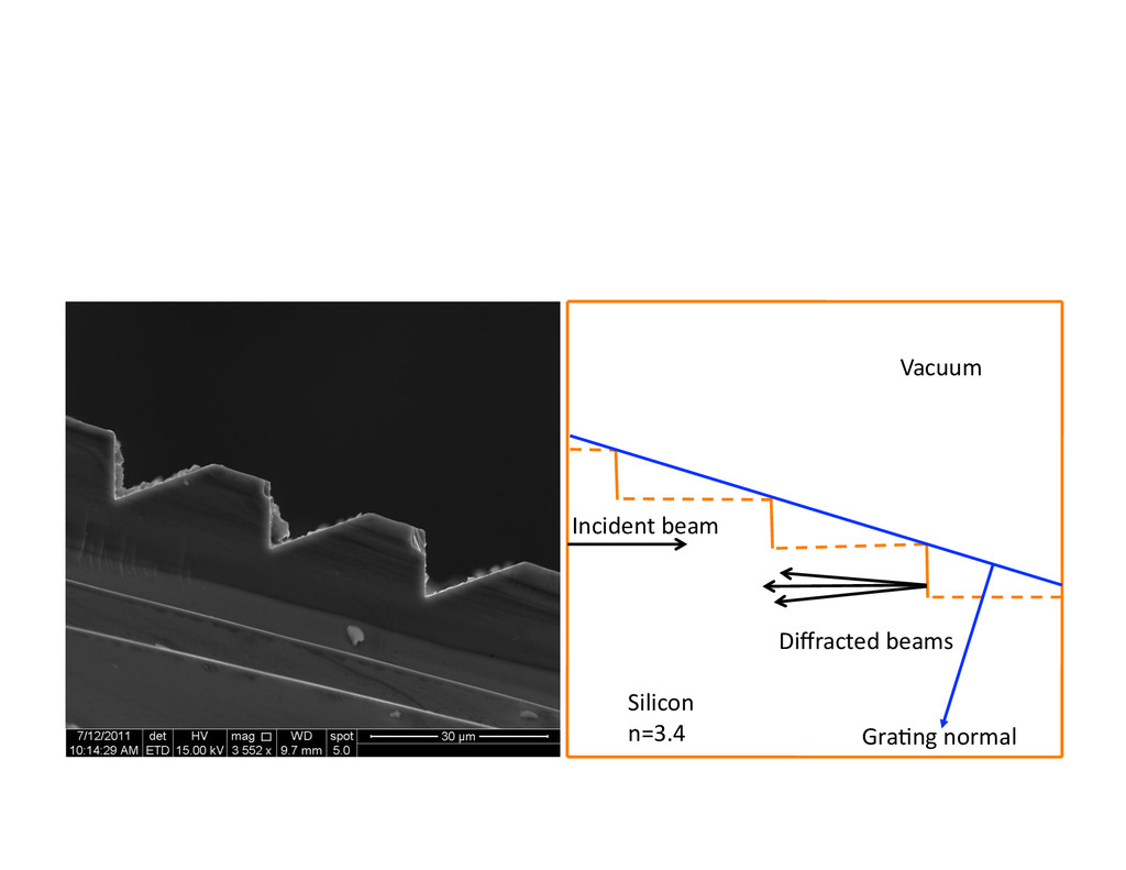
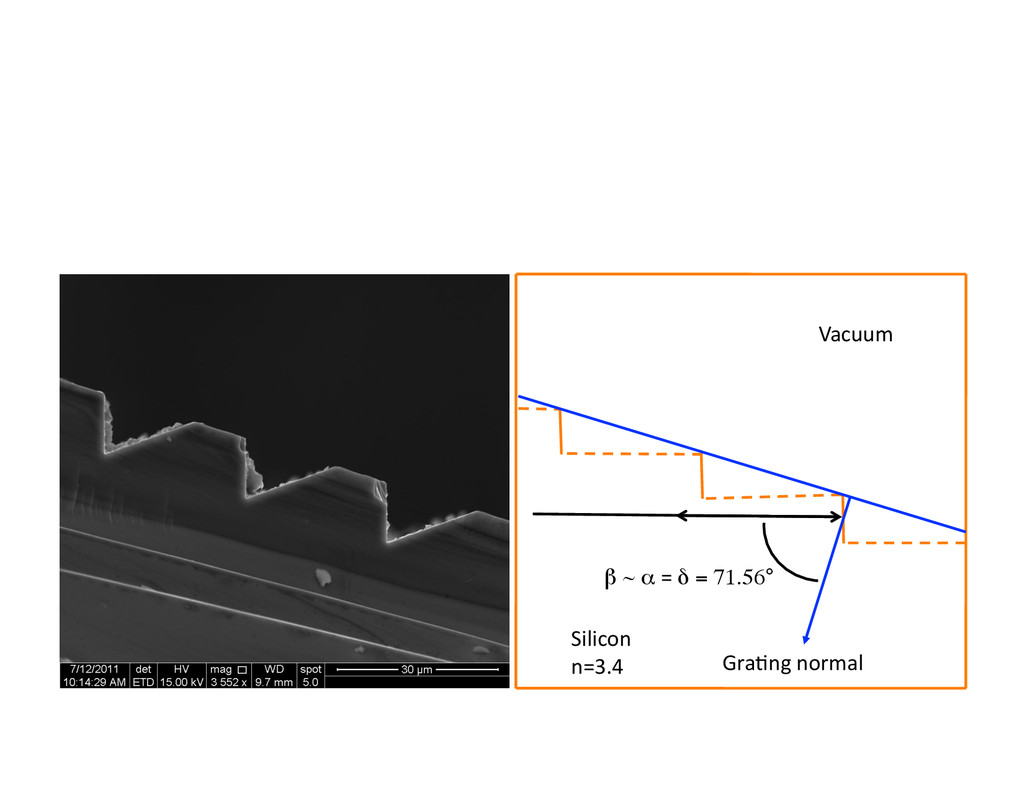
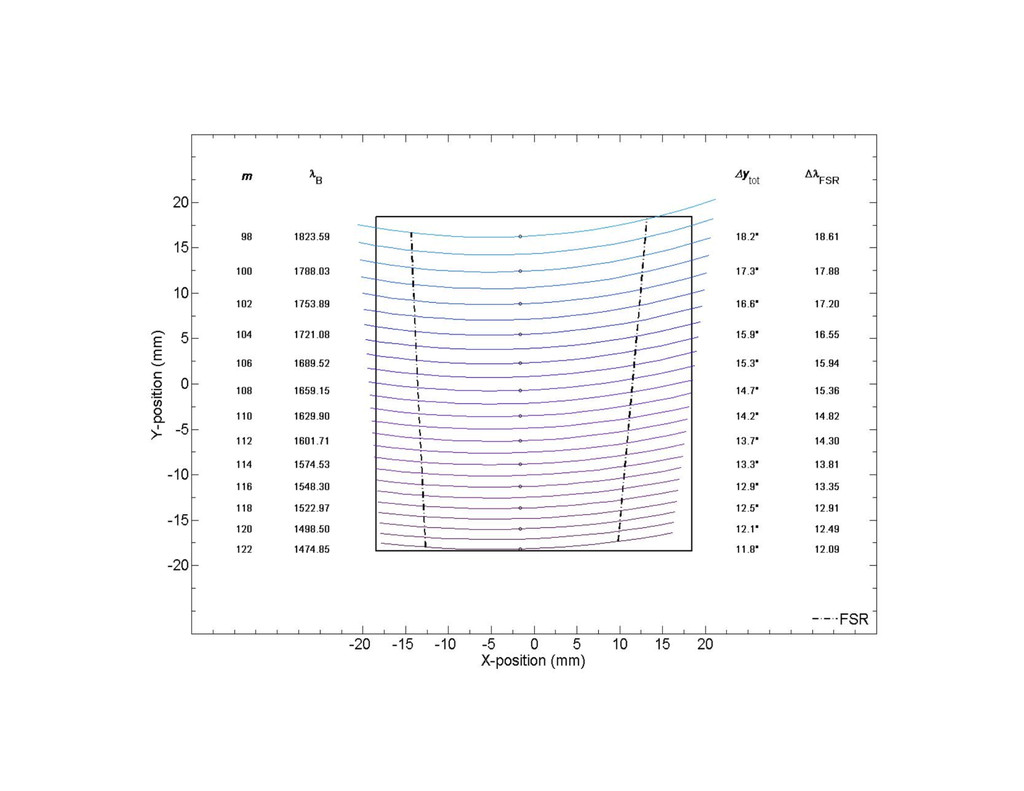
    blaze envelope angular width goes as Δθ = λ/w *The Free Spectral Range is the available bandwidth in a given order, it goes as Δλ = λ/ m On  the  next  slide  I  illustrate  how  diffracted  angles  depend  on  refrac0ve  index