Upgrade to Pro — share decks privately, control downloads, hide ads and more …

J601_lec02

 J601_lec02

5th Year, Integrated Technical Education Cluster AlAmeeria‎
lec#2, Electronic Principals (over twp weeks)

Ahmad El-Banna

October 26, 2014
Tweet

More Decks by Ahmad El-Banna

Other Decks in Education

Transcript

  1. Lecture #2 Diode Applications Instructor: Dr. Ahmad El-Banna October 2014

    J-601-1448 Electronic Principals Integrated Technical Education Cluster At AlAmeeria‎ © Ahmad El-Banna
  2. Agenda Load Line analysis Series, Parallel and Series-Parallel Configurations AND/OR

    Gates Half and Full-wave Rectification Clippers, Clampers and Zener Diodes Voltage-Multiplier Circuits Practical Applications 2 J-601-1448 , Lec#2 , Oct 2014 © Ahmad El-Banna
  3. Introduction • This lecture will develop a working knowledge of

    the diode in a variety of configurations using models appropriate for the area of application. • Once the basic behavior of a device is understood, its function and response in an infinite variety of configurations can be examined. • The analysis of electronic circuits can follow one of two paths: using the actual characteristics or applying an approximate model for the device. 3 J-601-1448 , Lec#2 , Oct 2014 © Ahmad El-Banna
  4. Load Line Analysis 5 J-601-1448 , Lec#2 , Oct 2014

    © Ahmad El-Banna • the load line is determined simply by the applied network, whereas the characteristics are defined by the chosen device. The intersections of the load line on the characteristics can be determined by first applying Kirchhoff’s voltage law in the clockwise direction • Solving for VD • Solving for ID
  5. Series Diode Configuration • It’s assumed that the forward resistance

    of the diode is usually so small compared to the other series elements of the network that it can be ignored. • In general, a diode is in the “on” state if the current established by the applied sources is such that its direction matches that of the arrow in the diode symbol, and VD ≥ 0.7V for silicon, VD ≥ 0.3V for germanium, and VD ≥ 1.2V for gallium arsenide. 8 J-601-1448 , Lec#2 , Oct 2014 © Ahmad El-Banna
  6. Parallel Configuration 10 J-601-1448 , Lec#2 , Oct 2014 ©

    Ahmad El-Banna What about blue LED? Design Problem
  7. AND/OR Gate • Positive logic: Logic 1 E volt ,

    Logic 0  0 volt 13 J-601-1448 , Lec#2 , Oct 2014 © Ahmad El-Banna Positive logic AND gate Positive logic OR gate Vi1 Vi2 Vo 0 0 0 0 1 1 1 0 1 1 1 1 Vi1 Vi2 Vo 0 0 0 0 1 0 1 0 0 1 1 1
  8. Half-wave Rectifier 15 J-601-1448 , Lec#2 , Oct 2014 ©

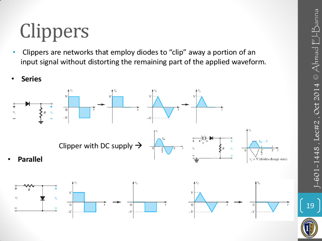
    Ahmad El-Banna • Effect of VK on half-wave rectified signal. Cross Over distortion The process of removing one-half the input signal to establish a dc level is called half-wave rectification.
  9. Center-tapped transformer full-wave rectifier 17 J-601-1448 , Lec#2 , Oct

    2014 © Ahmad El-Banna • Center-tapped transformer full-wave rectifier. Determining Vo max for diodes in the bridge configuration
  10. Clippers • Clippers are networks that employ diodes to “clip”

    away a portion of an input signal without distorting the remaining part of the applied waveform. 19 J-601-1448 , Lec#2 , Oct 2014 © Ahmad El-Banna • Series • Parallel Clipper with DC supply 
  11. Clampers 21 J-601-1448 , Lec#2 , Oct 2014 © Ahmad

    El-Banna Clamping network with a sinusoidal input. A clamper is a network constructed of a diode, a resistor, and a capacitor that shifts a waveform to a different dc level without changing the appearance of the applied signal.
  12. Networks with a Dc and AC sources • The response

    of any network with both an ac and a dc source can be found by finding the response to each source independently and then combining the results. 22 J-601-1448 , Lec#2 , Oct 2014 © Ahmad El-Banna Load Line
  13. Zener Diodes 23 J-601-1448 , Lec#2 , Oct 2014 ©

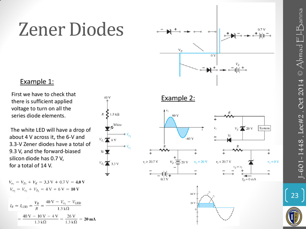
    Ahmad El-Banna Example 1: First we have to check that there is sufficient applied voltage to turn on all the series diode elements. The white LED will have a drop of about 4 V across it, the 6-V and 3.3-V Zener diodes have a total of 9.3 V, and the forward-biased silicon diode has 0.7 V, for a total of 14 V. Example 2:
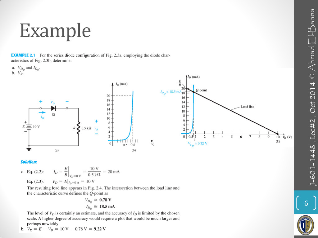
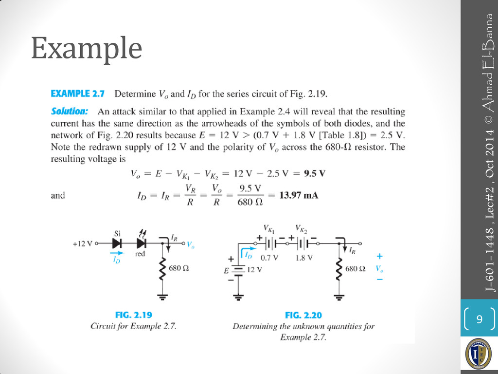
  14. Zener Diodes V i and R Fixed 24 J-601-1448 ,

    Lec#2 , Oct 2014 © Ahmad El-Banna 1. Determine the state of the Zener diode by removing it from the network and calculating the voltage across the resulting open circuit. 2. Substitute the appropriate equivalent circuit and solve for the desired unknowns.
  15. Zener Diodes Fixed V i , Variable R L 25

    J-601-1448 , Lec#2 , Oct 2014 © Ahmad El-Banna Example:
  16. Zener Diodes Fixed R L , Variable V i 26

    J-601-1448 , Lec#2 , Oct 2014 © Ahmad El-Banna
  17. Voltage Doubler 28 J-601-1448 , Lec#2 , Oct 2014 ©

    Ahmad El-Banna • Half wave voltage doubler • Full wave voltage doubler
  18. Display 36 J-601-1448 , Lec#2 , Oct 2014 © Ahmad

    El-Banna Settings Voltage Reference levels
  19. Establishing a Voltage Level Insensitive to the Load Current 37

    J-601-1448 , Lec#2 , Oct 2014 © Ahmad El-Banna
  20. • For more details, refer to: • Chapter 2, Electronic

    Devices and Circuits, Boylestad. • The lecture is available online at: • https://speakerdeck.com/ahmad_elbanna • For inquires, send to: • [email protected][email protected] 39 J-601-1448 , Lec#2 , Oct 2014 © Ahmad El-Banna