Upgrade to Pro — share decks privately, control downloads, hide ads and more …

Row Hammer - Papers We Love

Row Hammer - Papers We Love

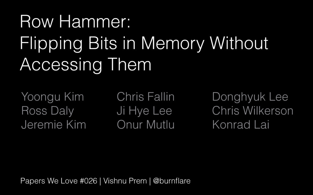
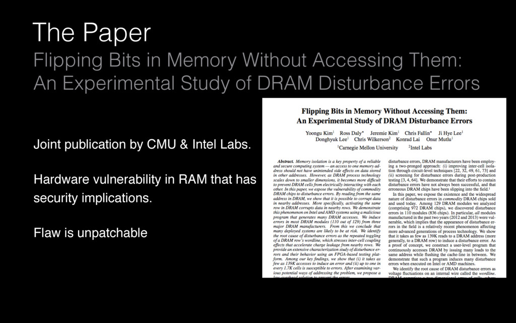
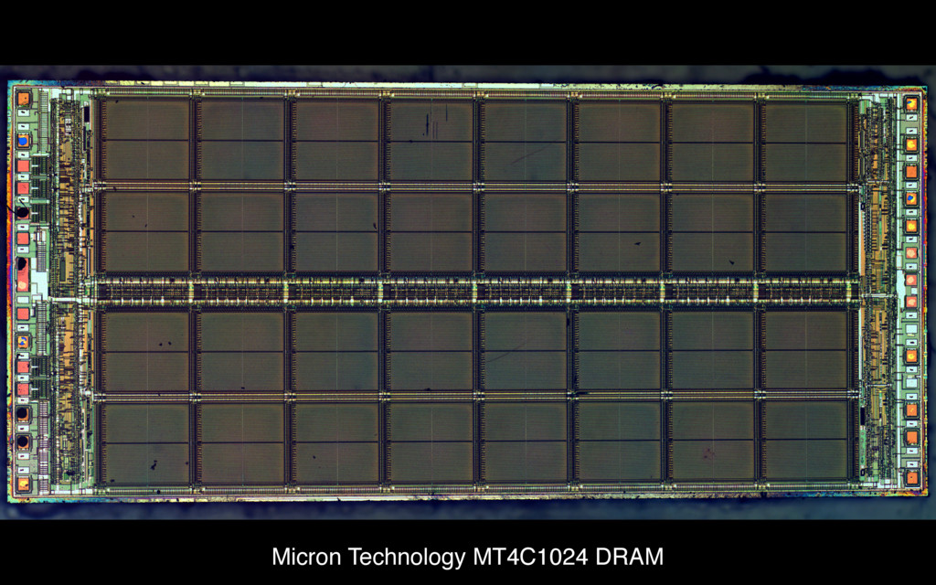
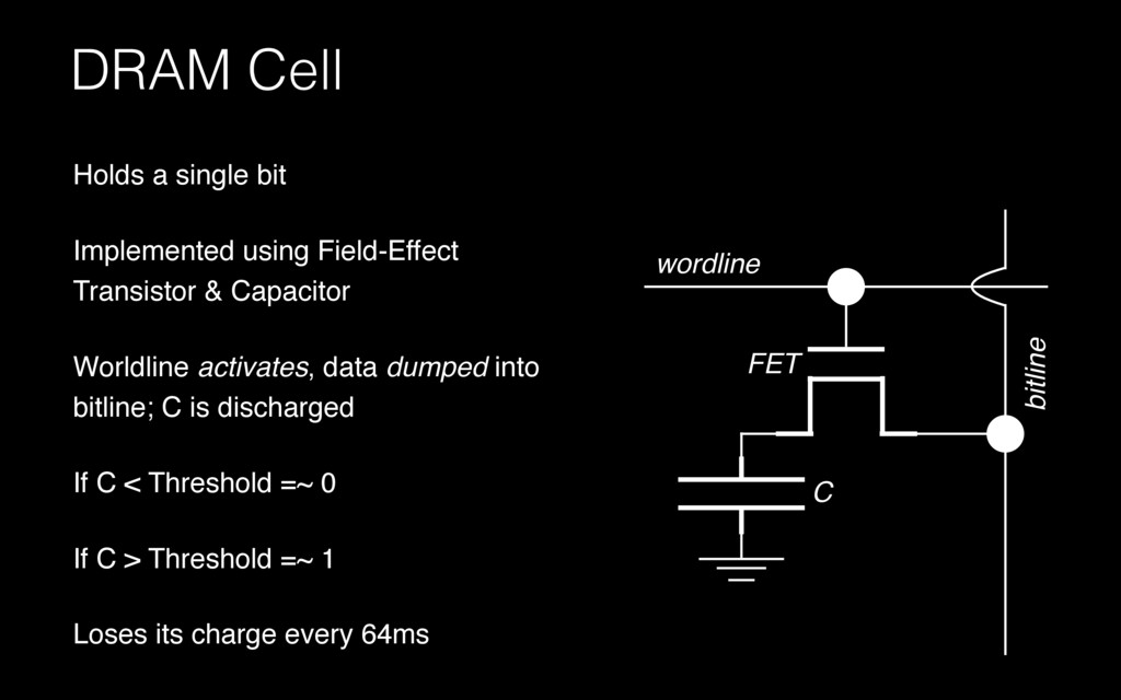
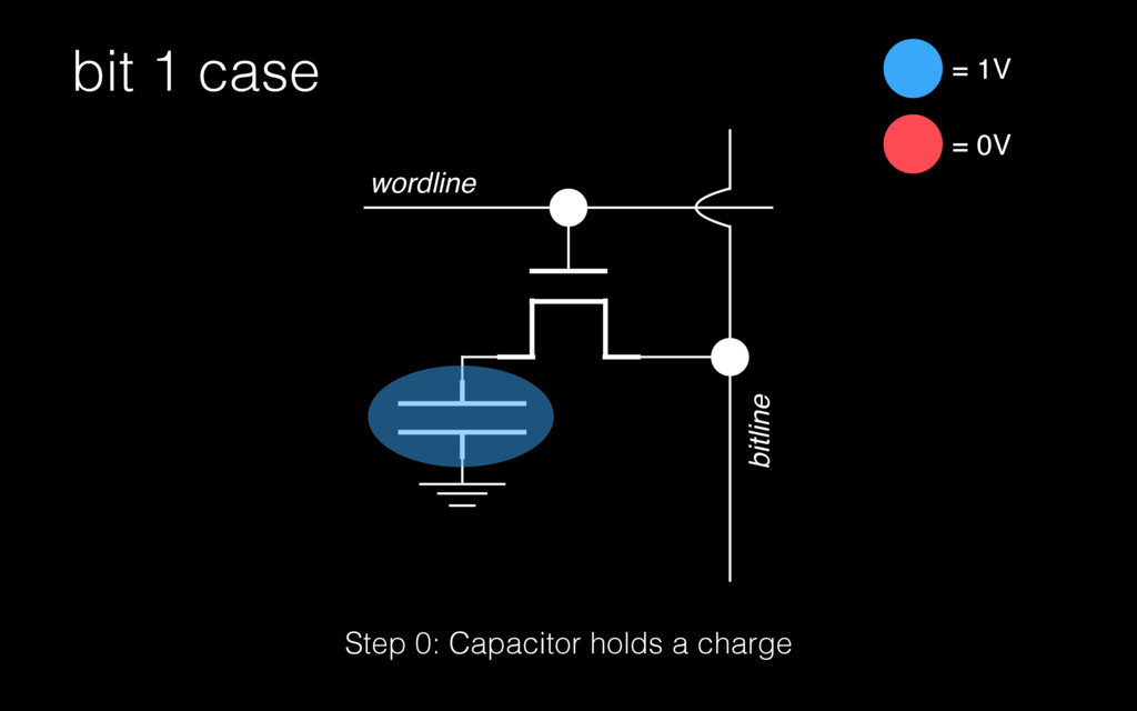
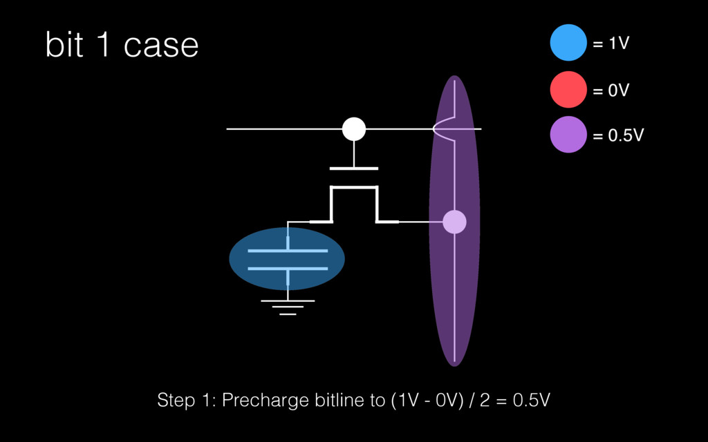
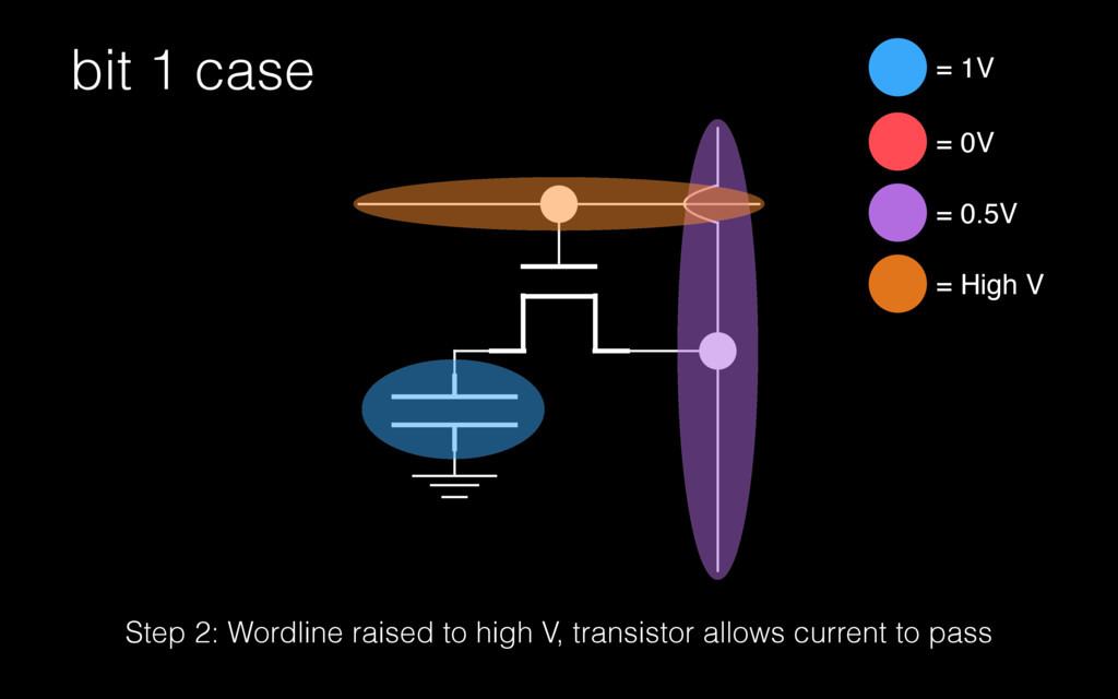
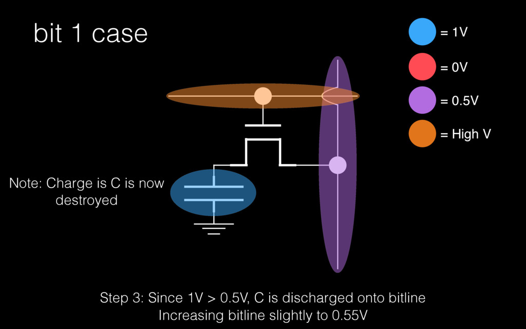
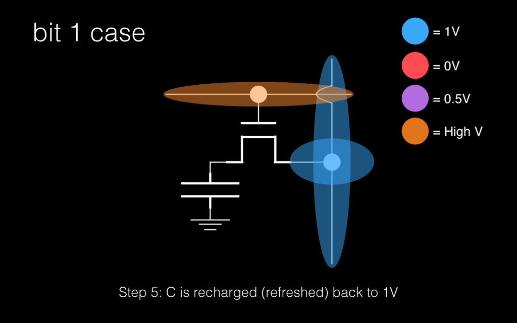
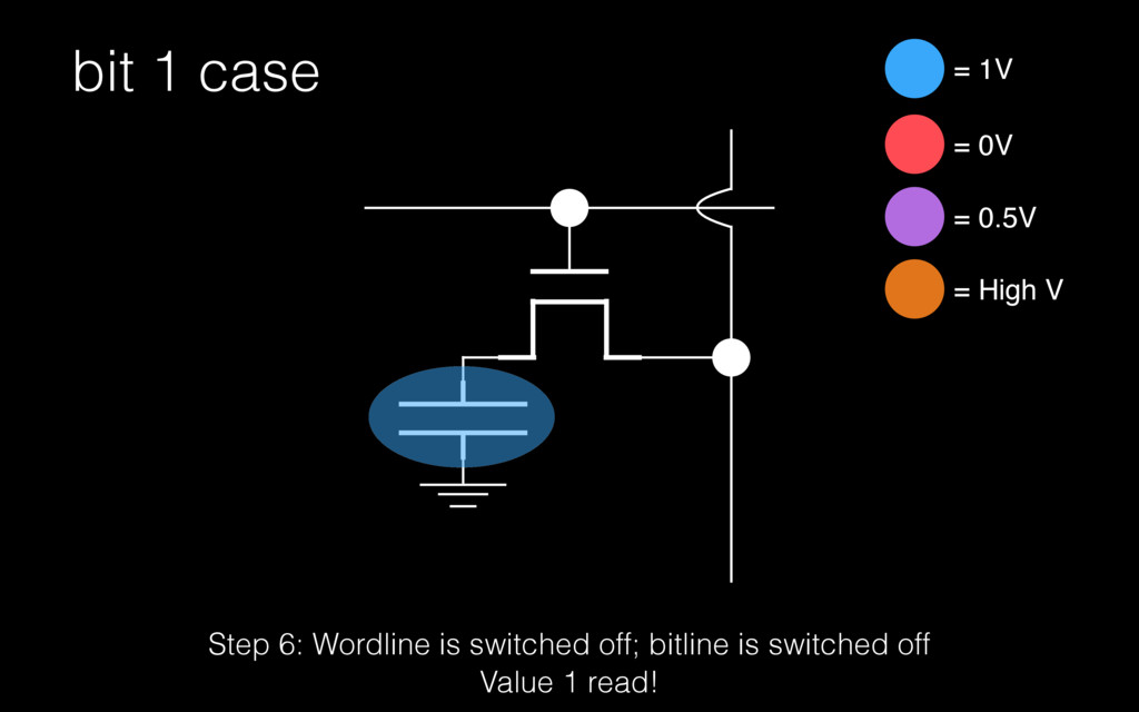
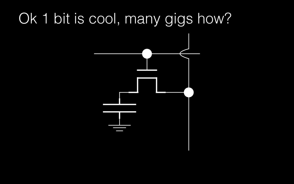
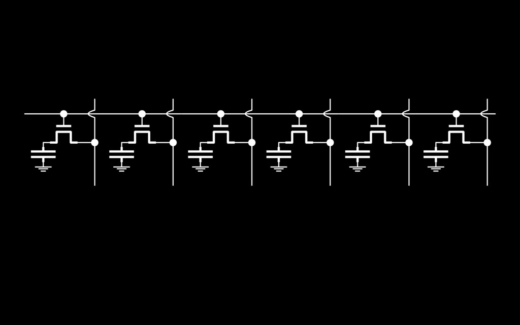
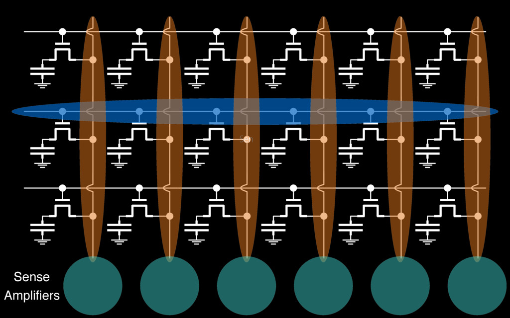
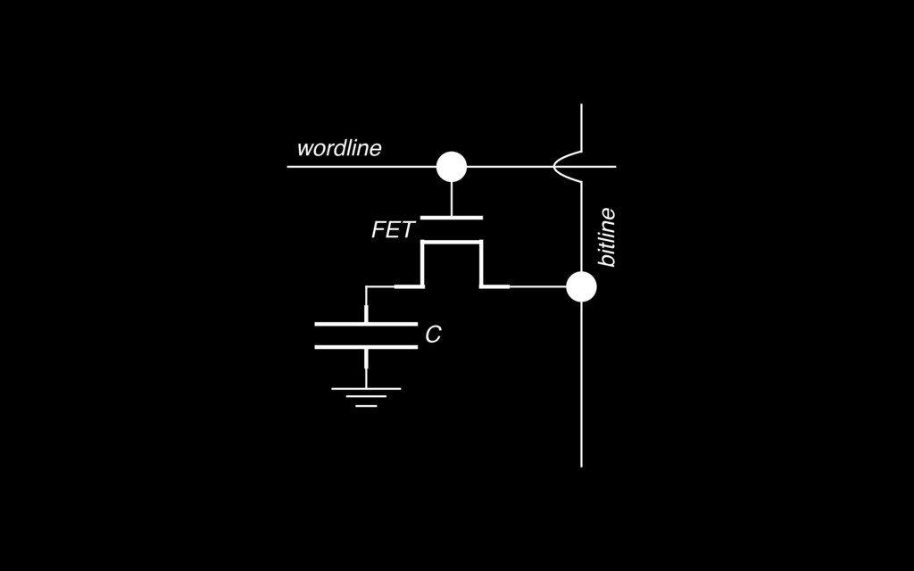
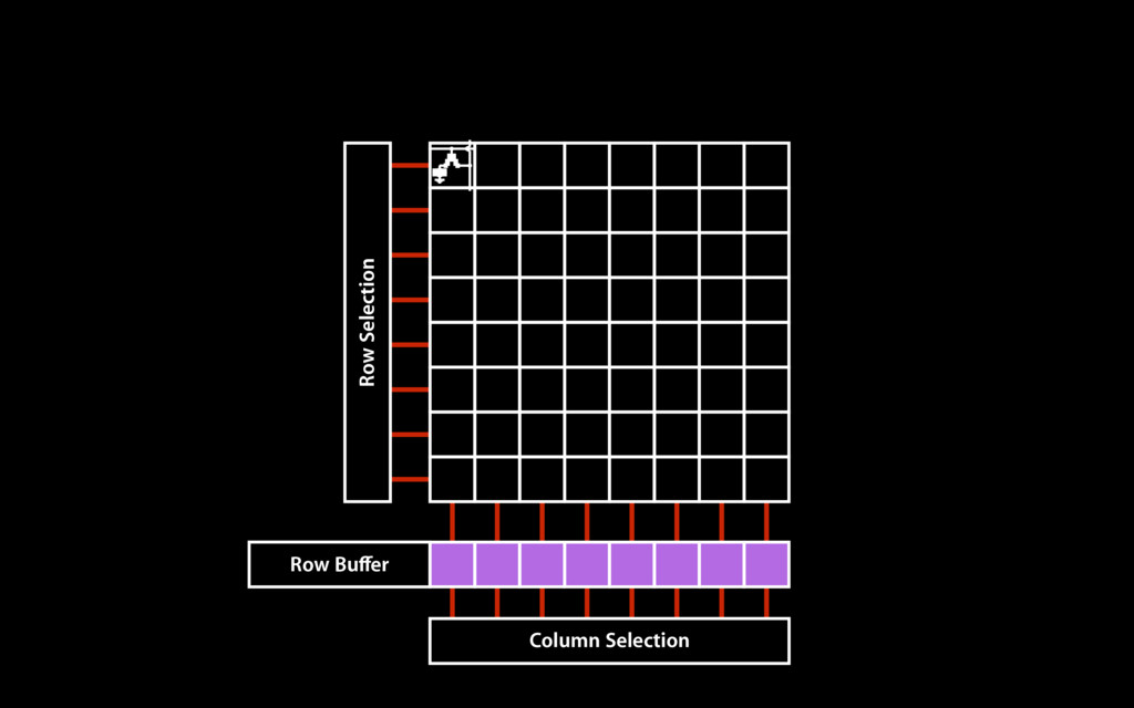
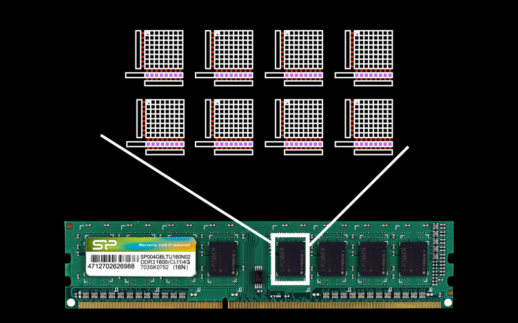
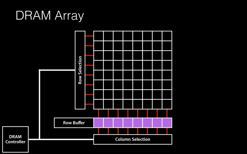
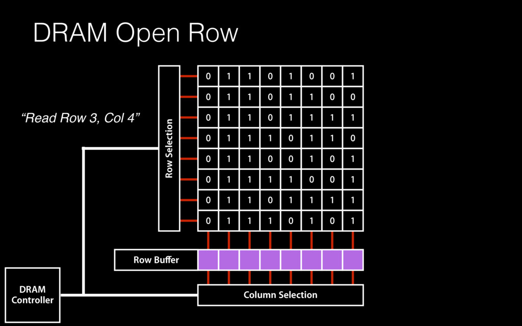
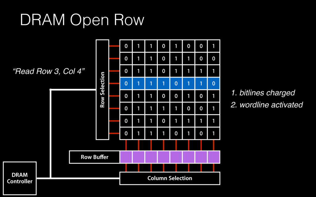
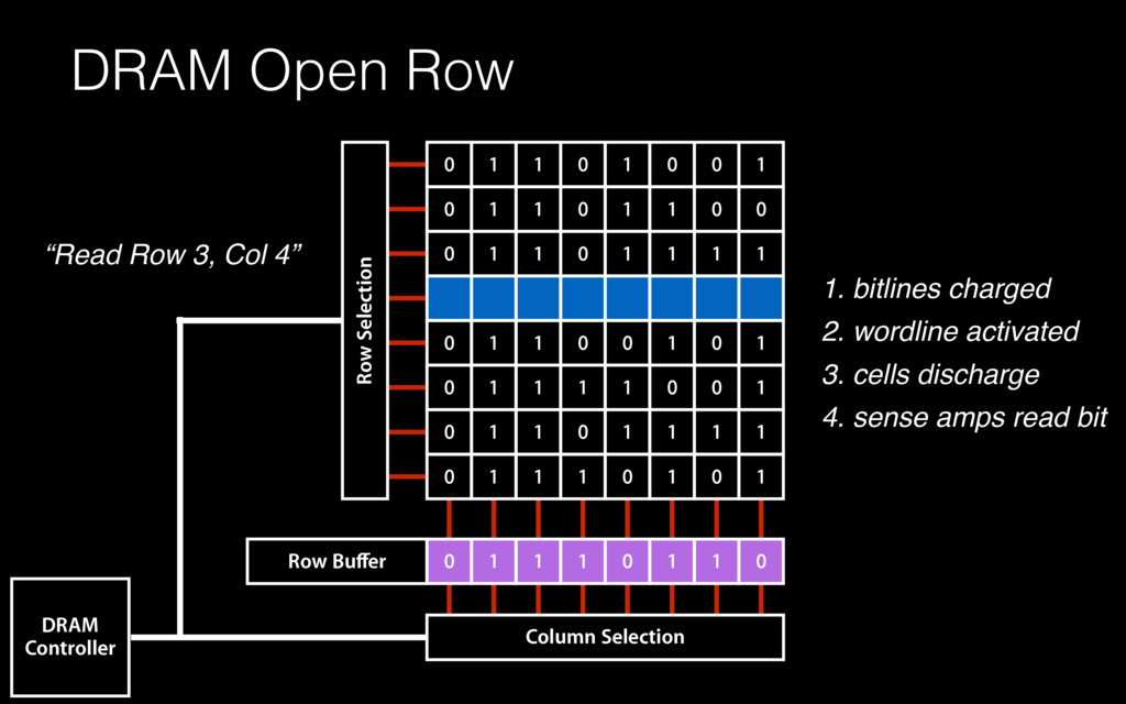
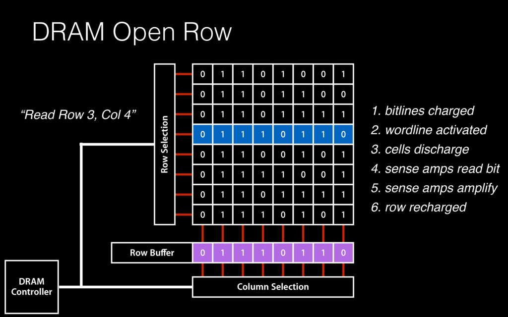
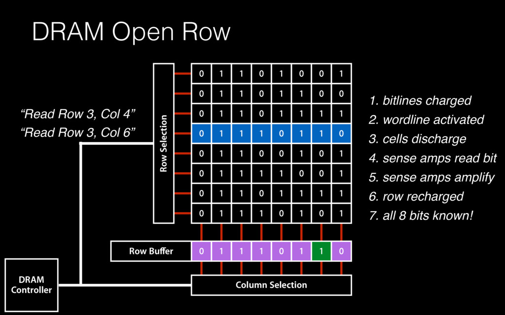
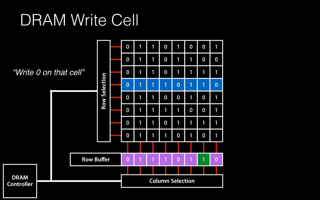
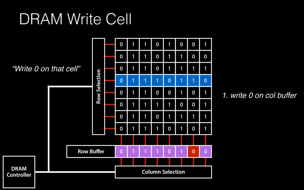
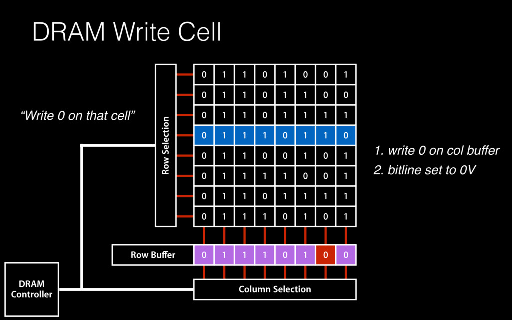
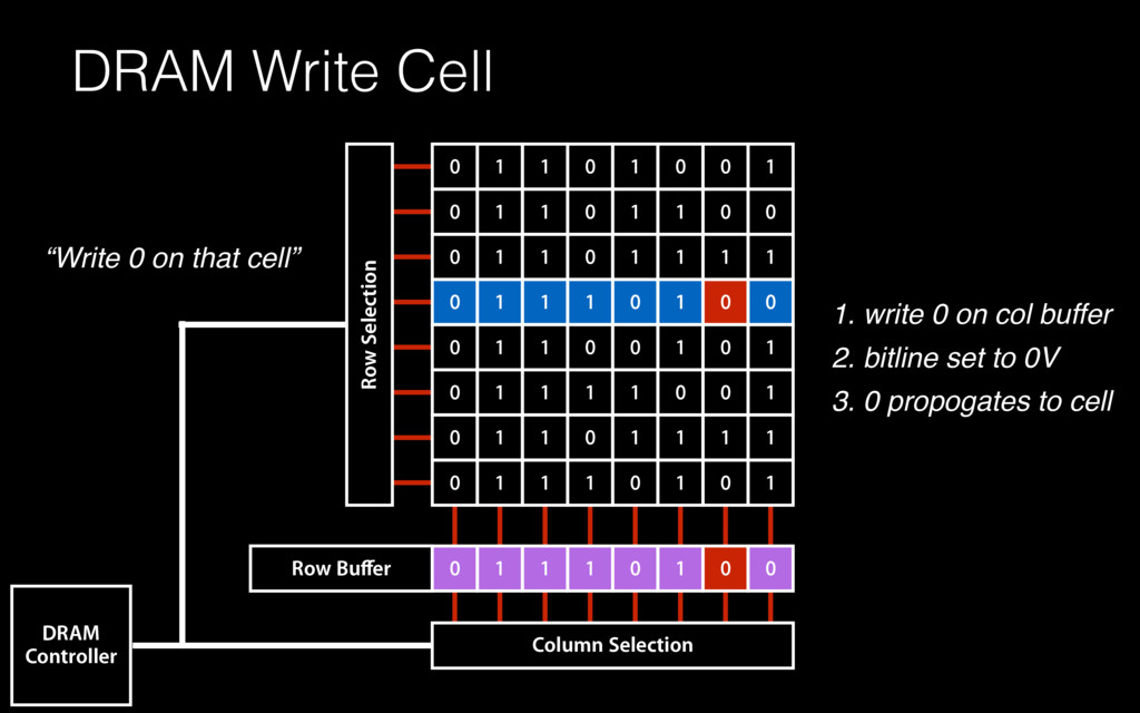
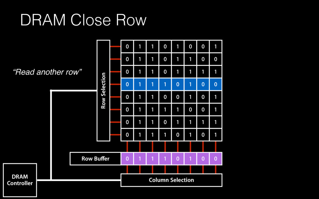
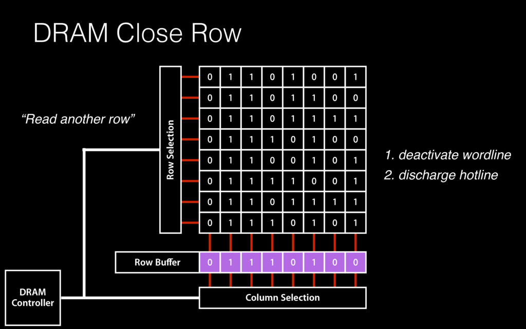
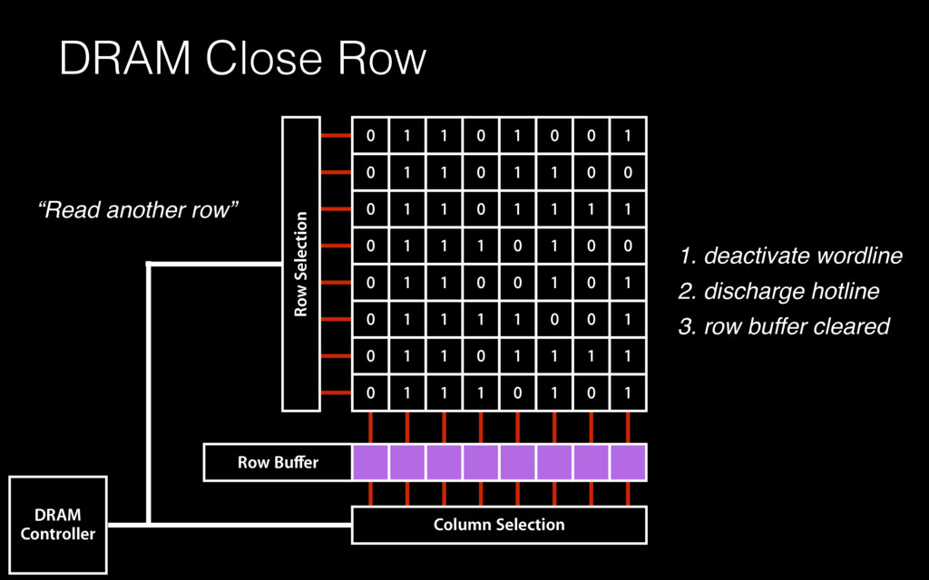
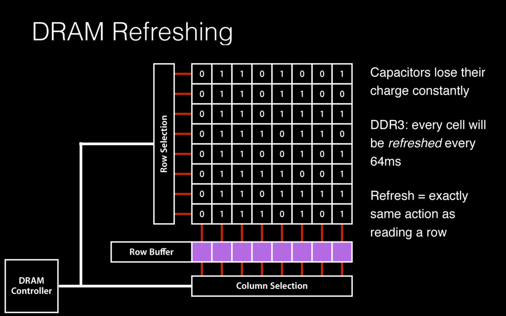
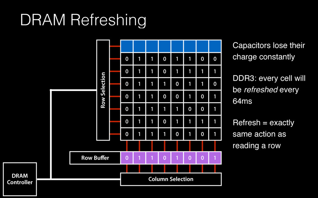
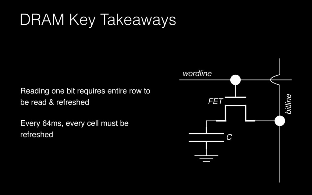
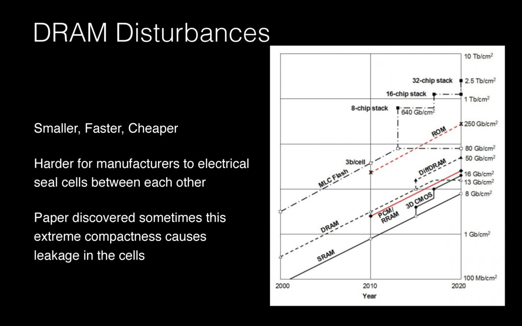
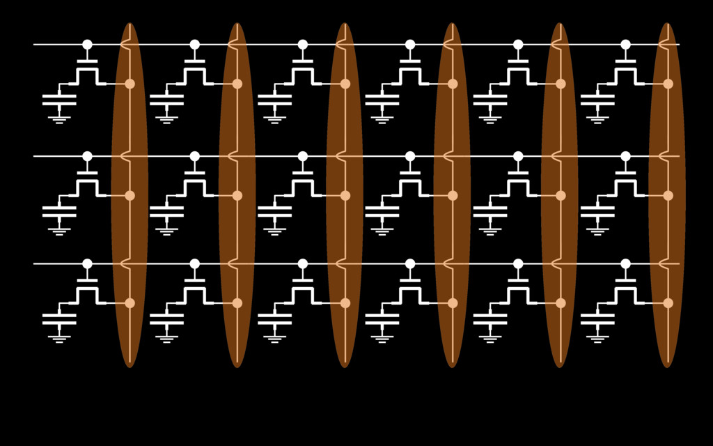
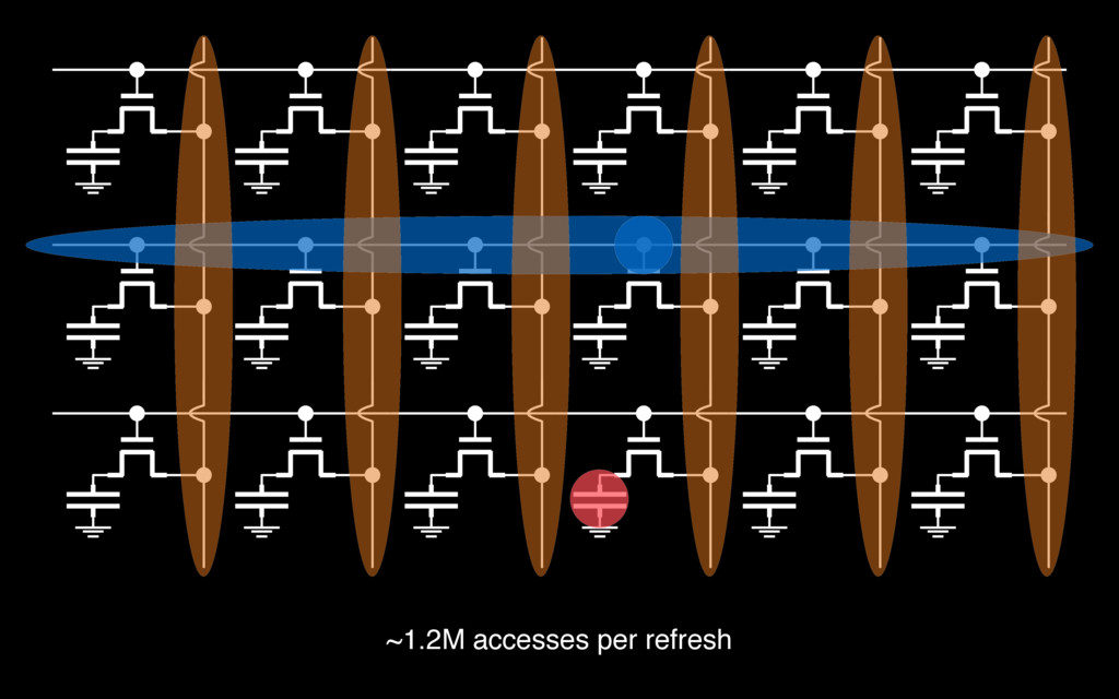
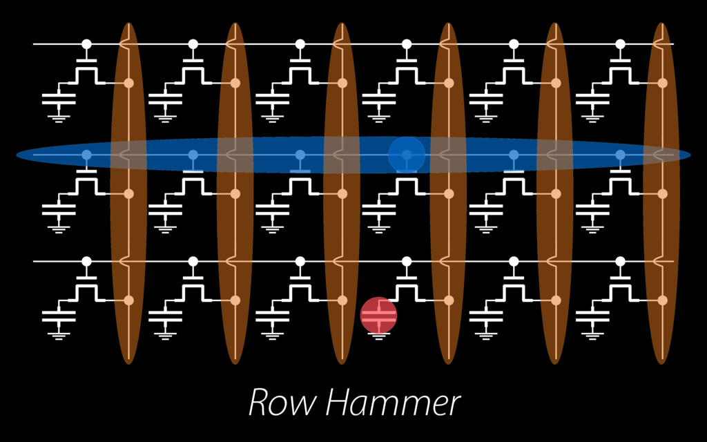
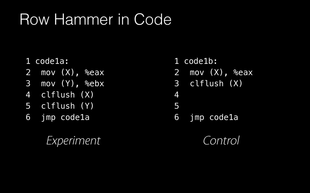
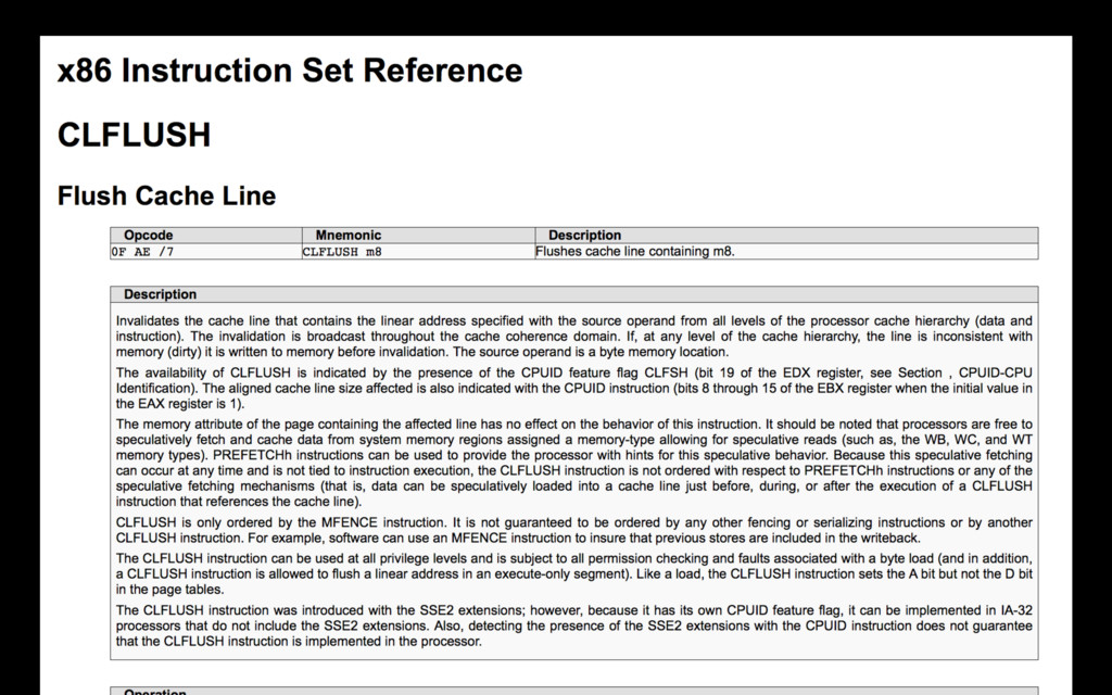
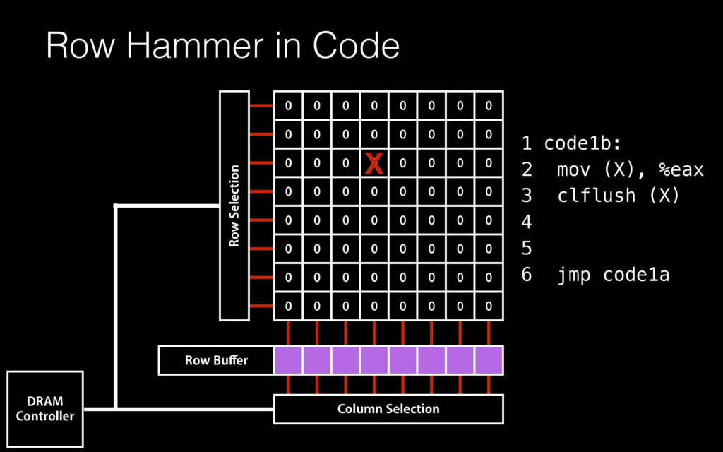
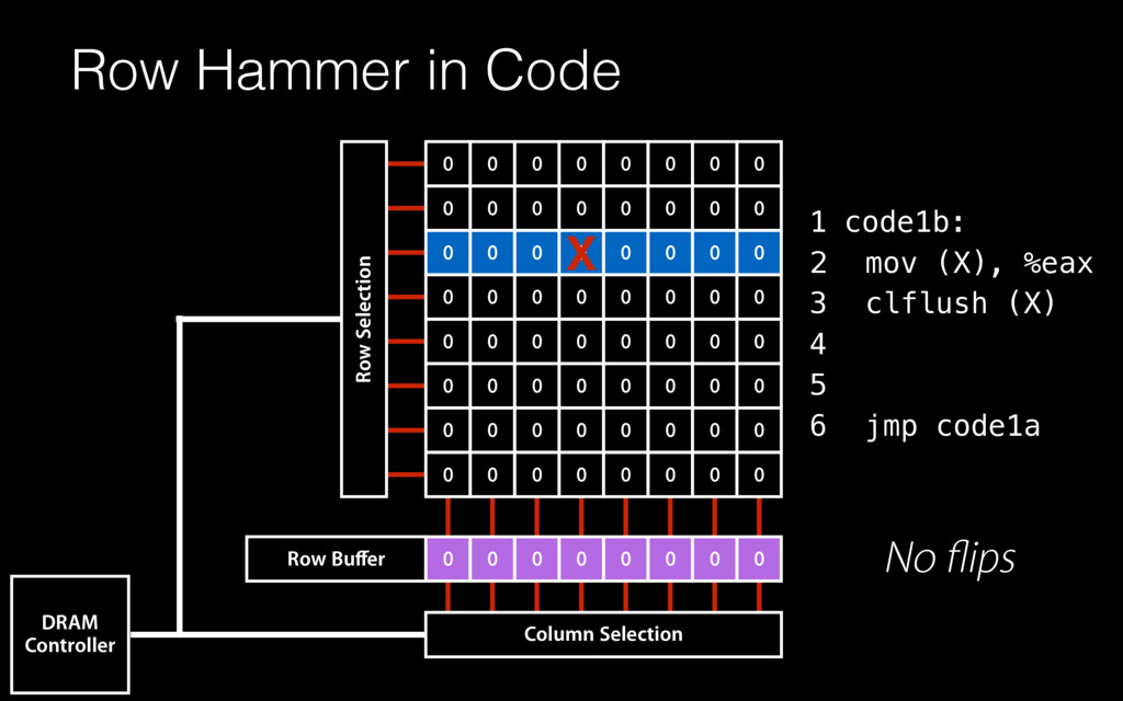
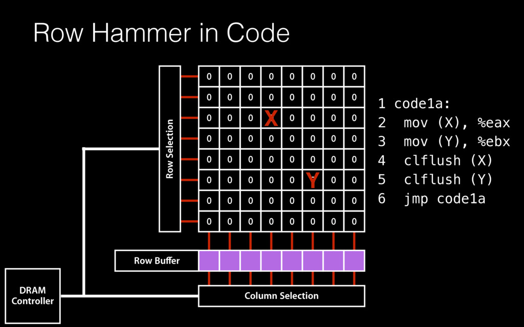
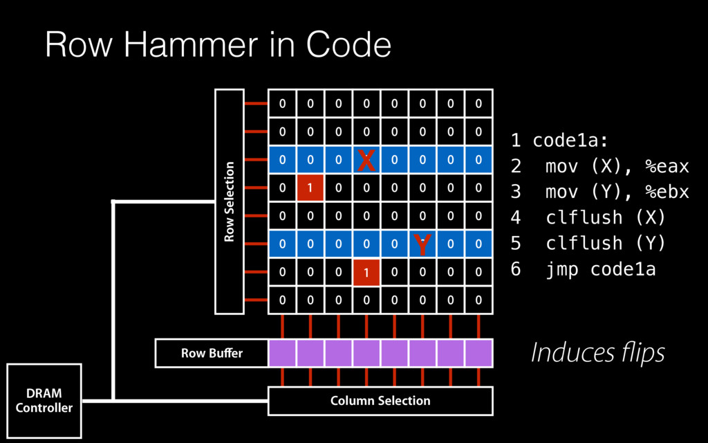
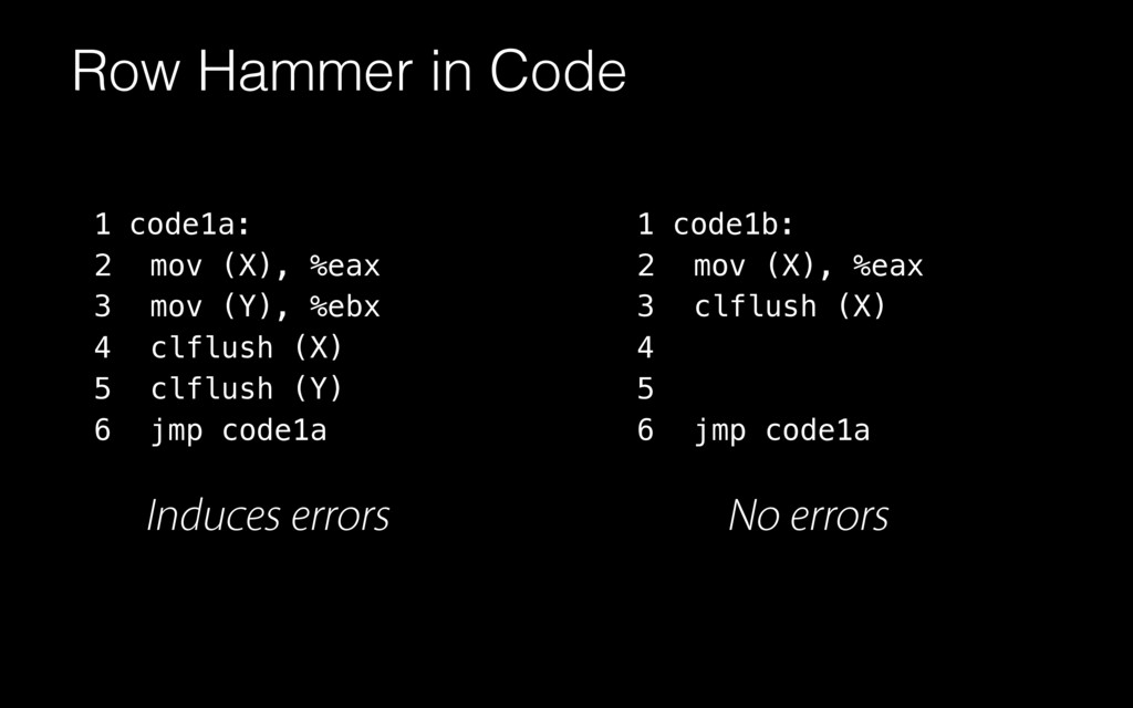
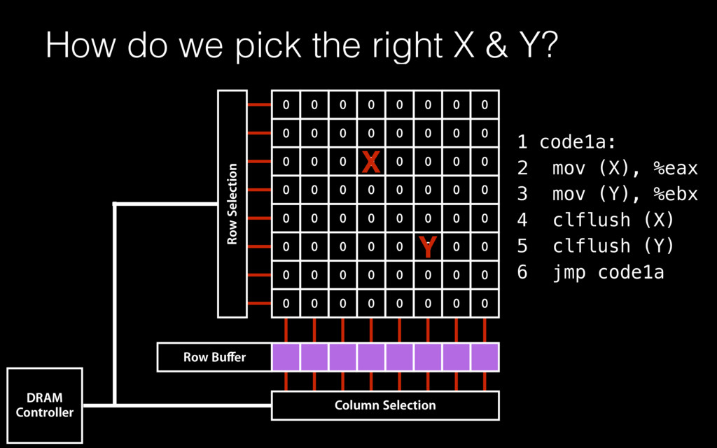
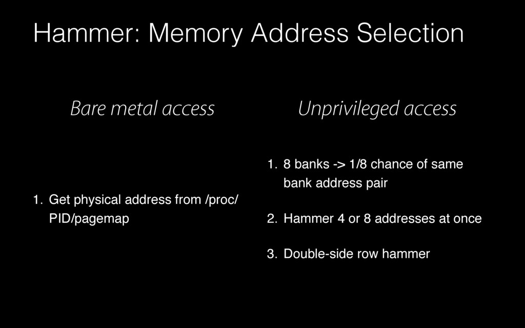
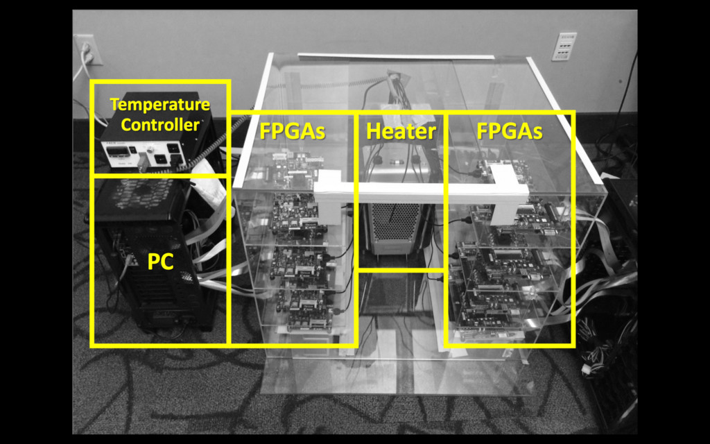
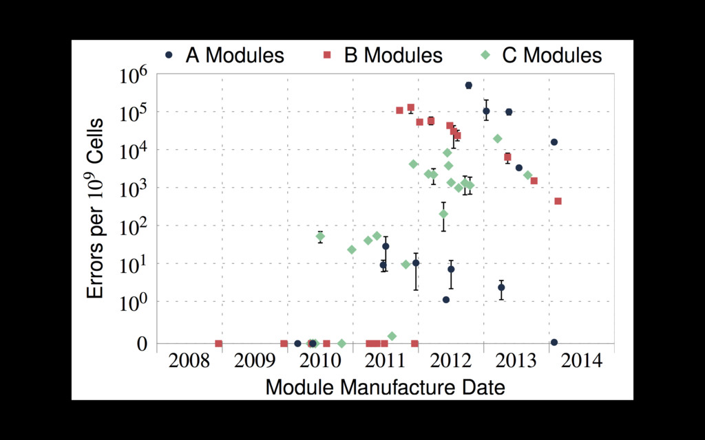
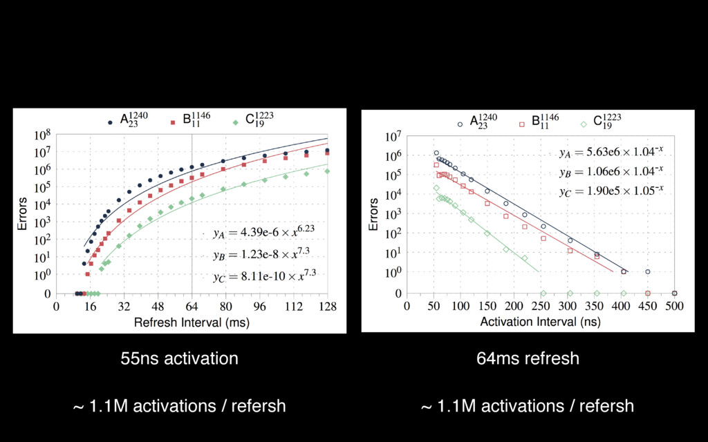
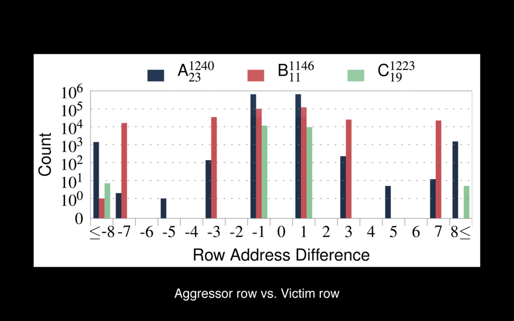
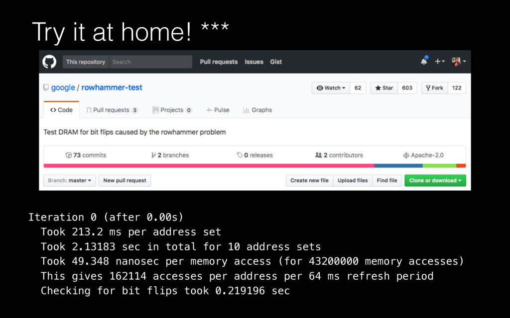
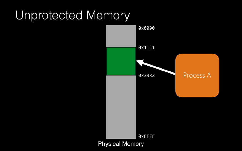
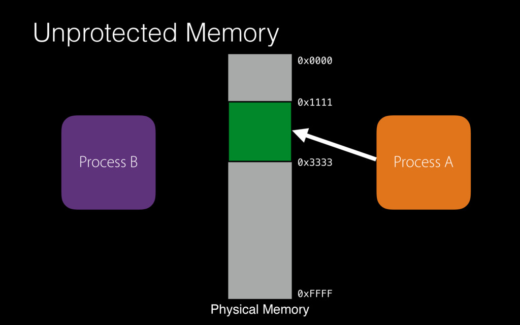
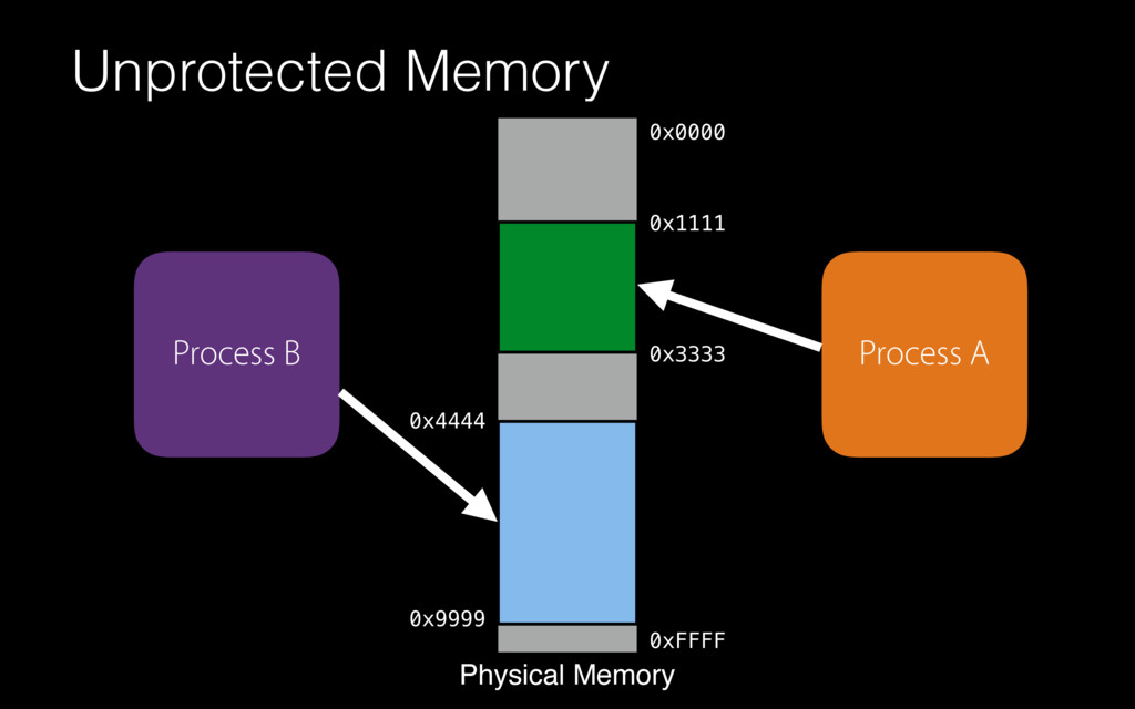
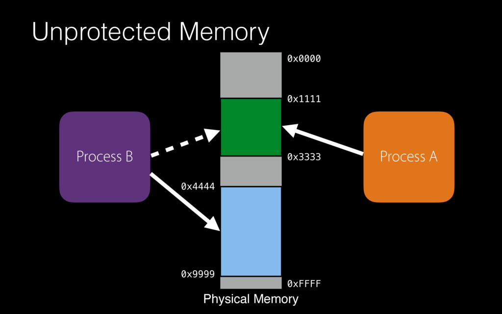
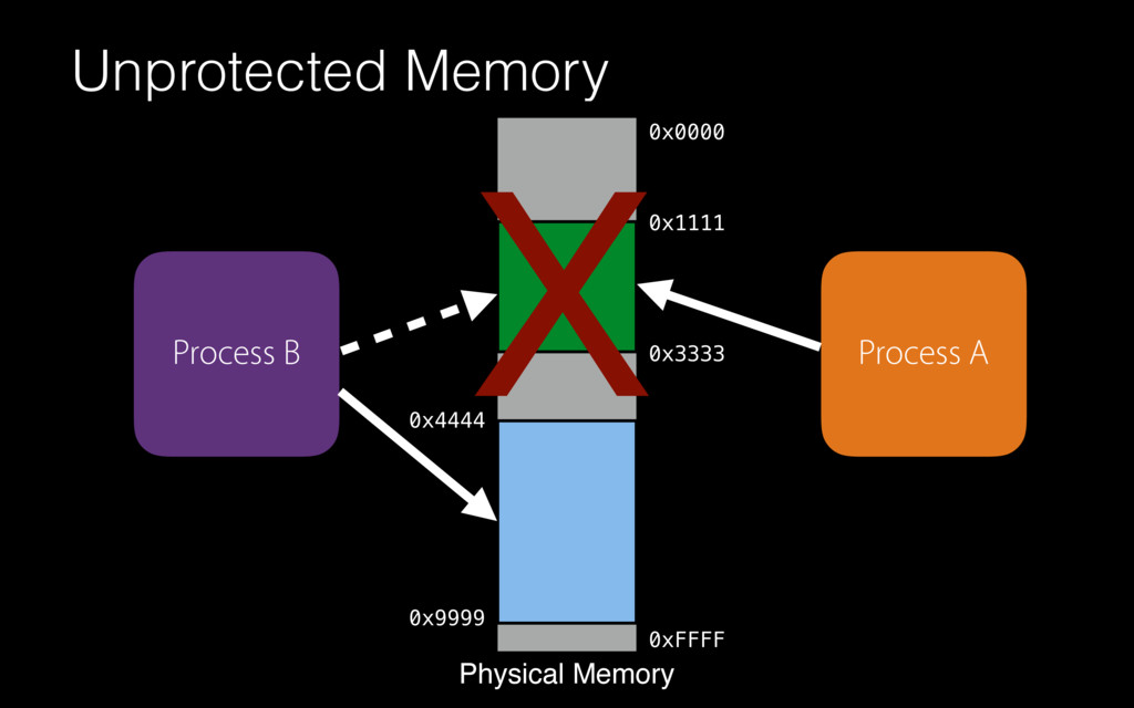
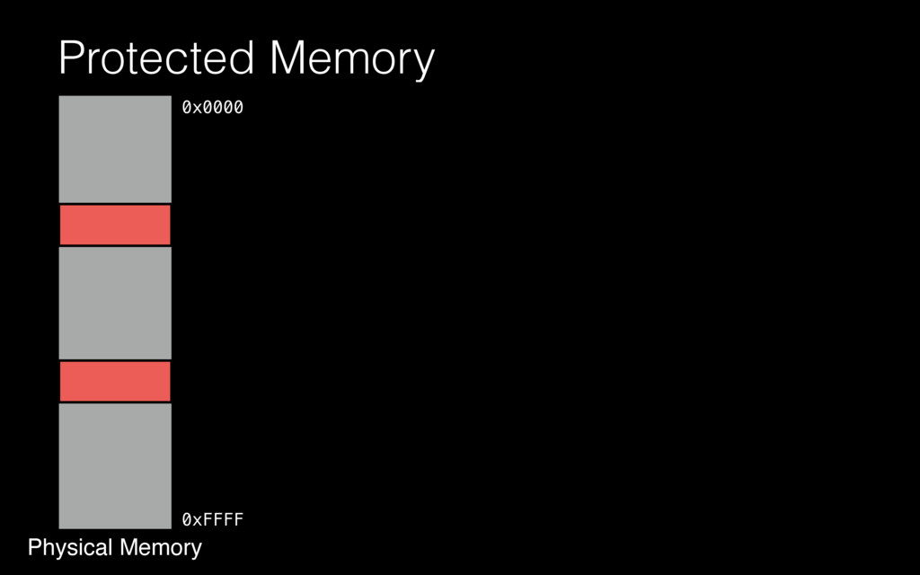
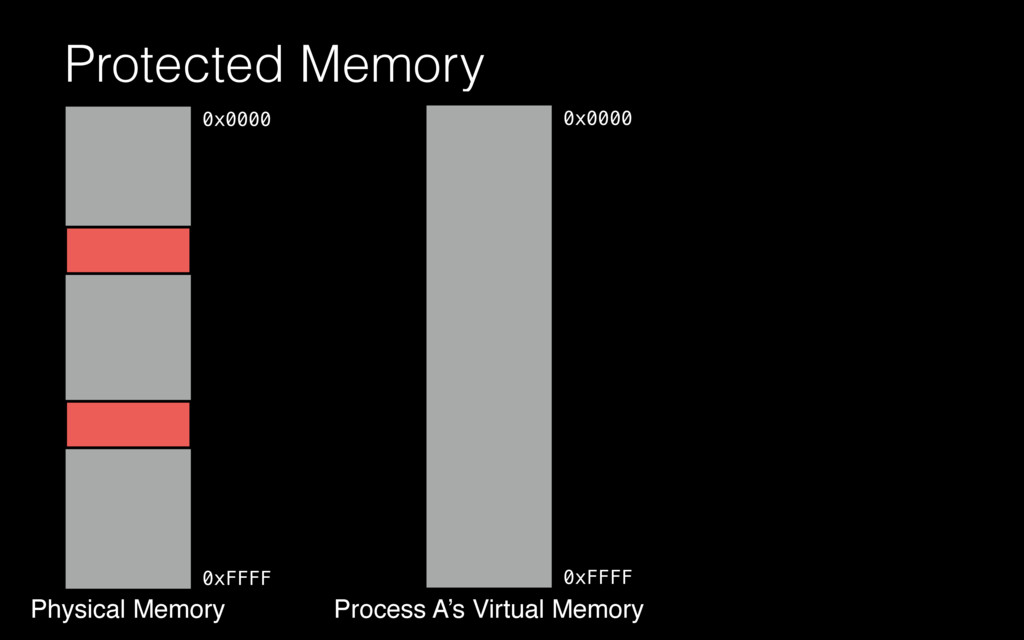
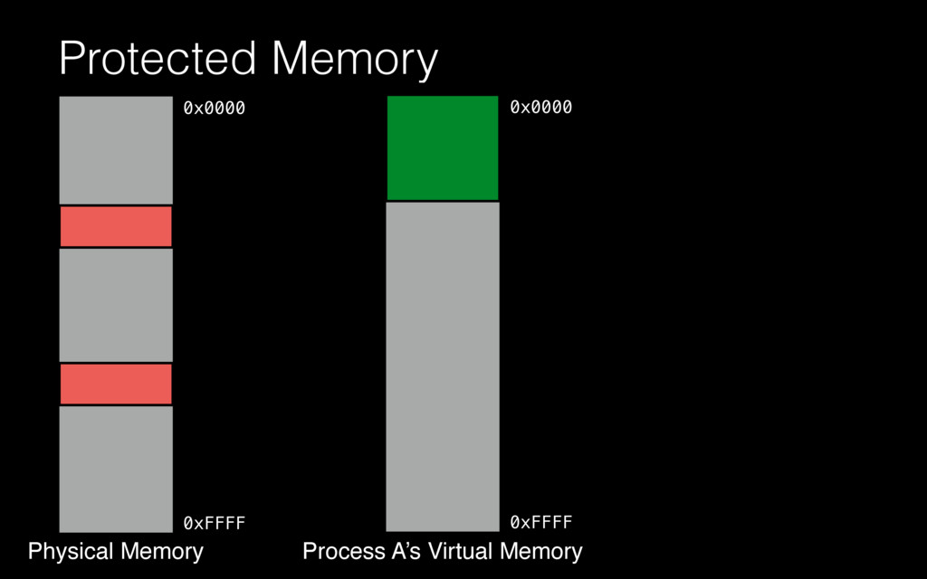
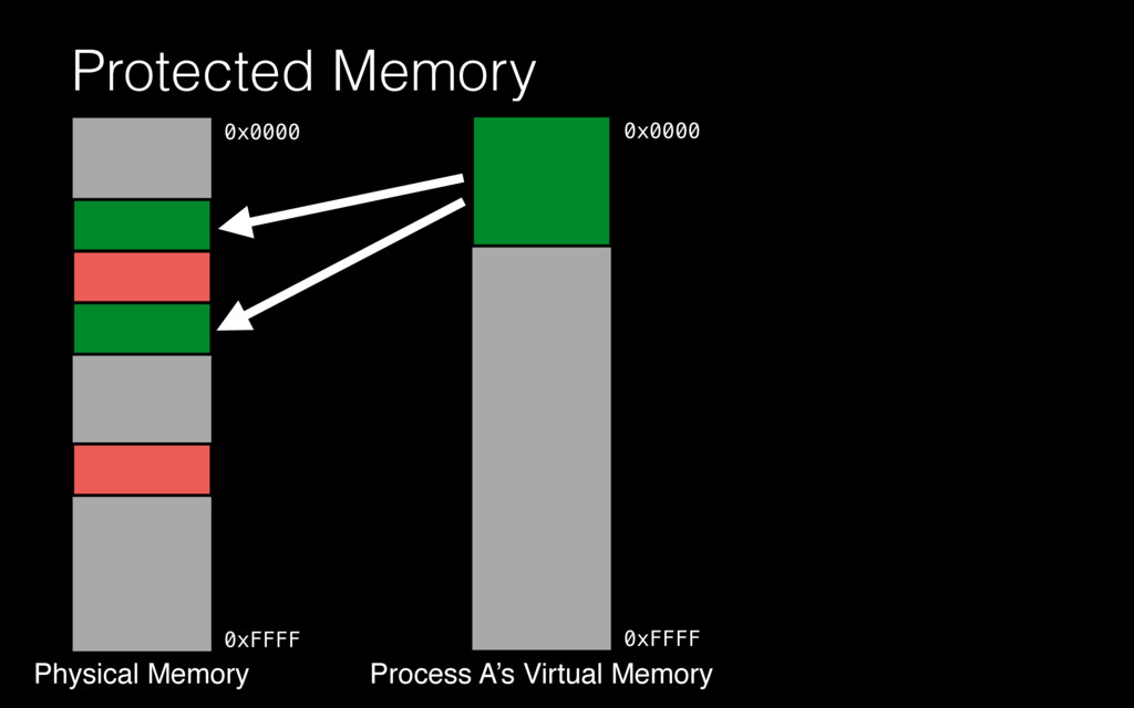
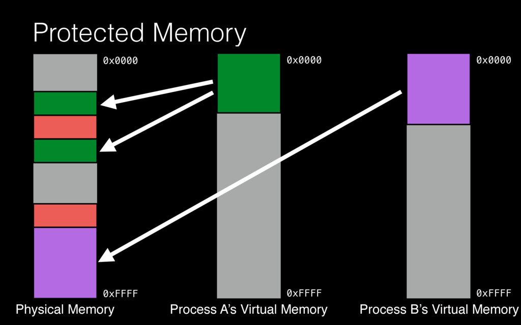
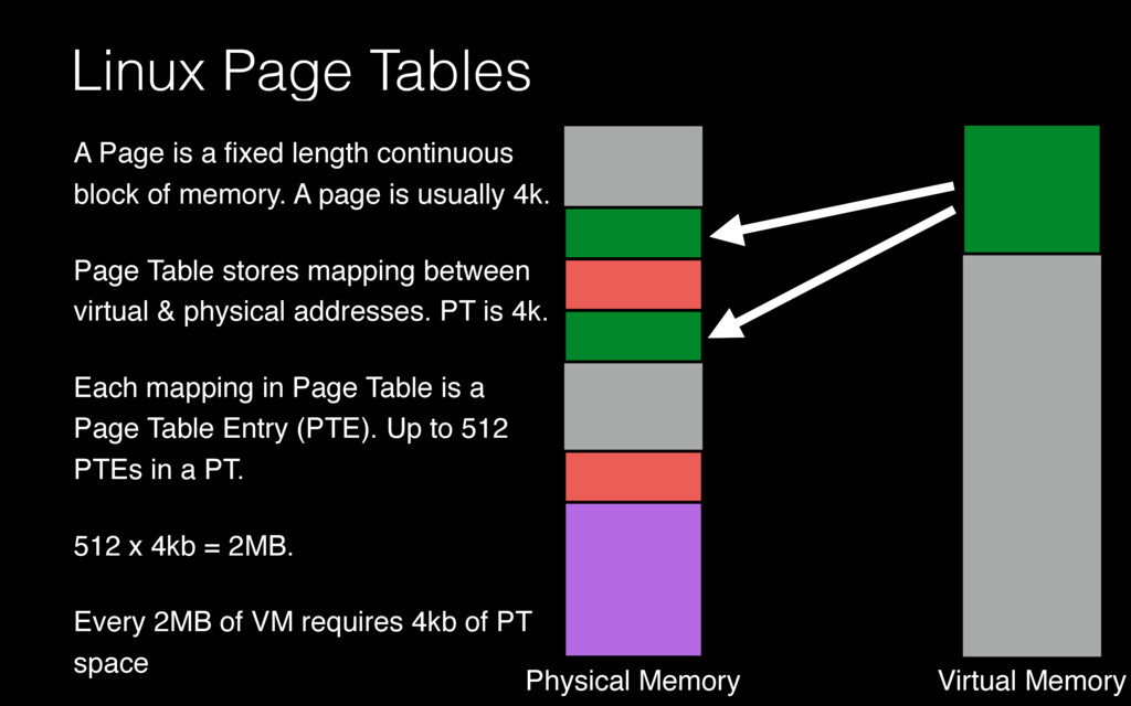
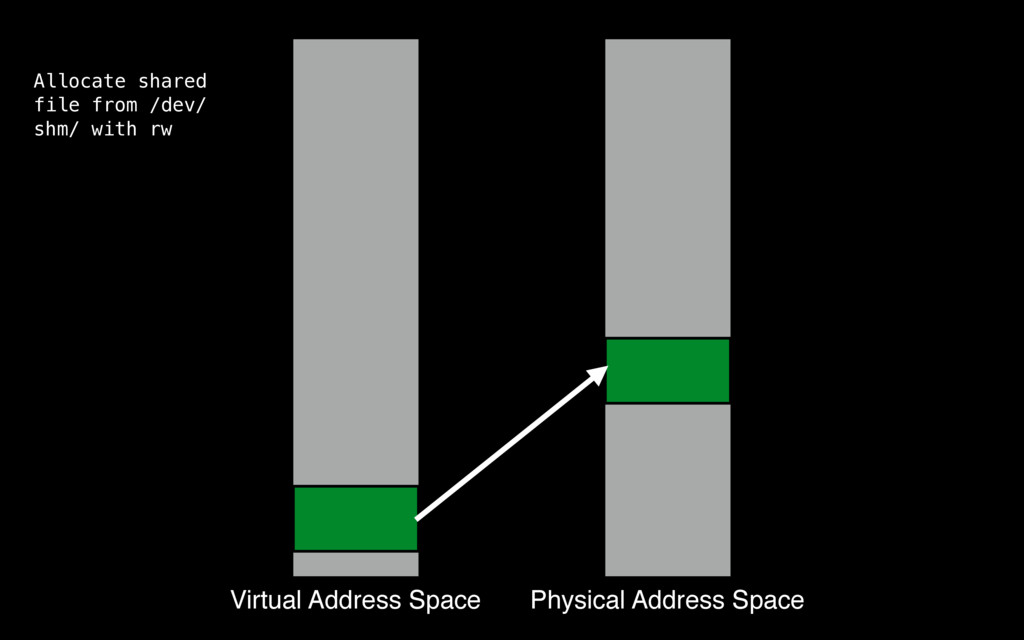
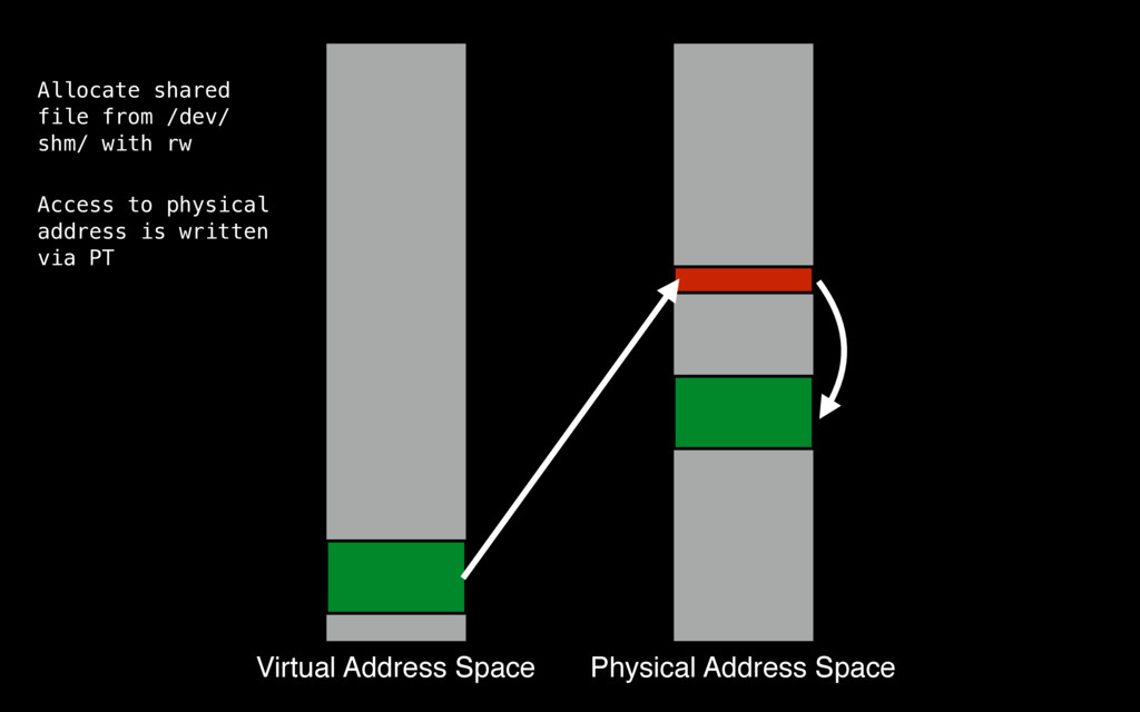
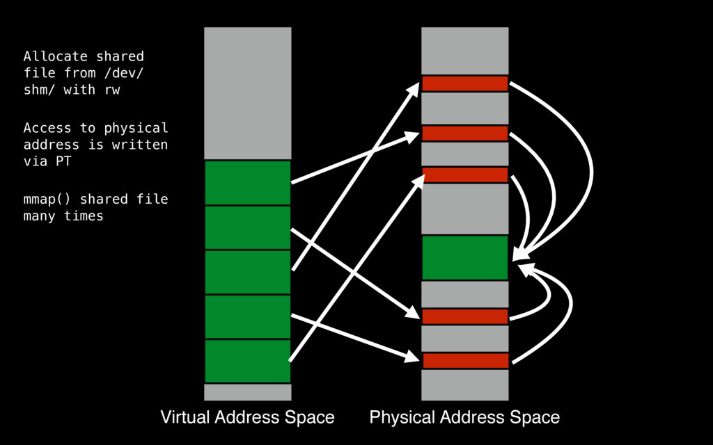
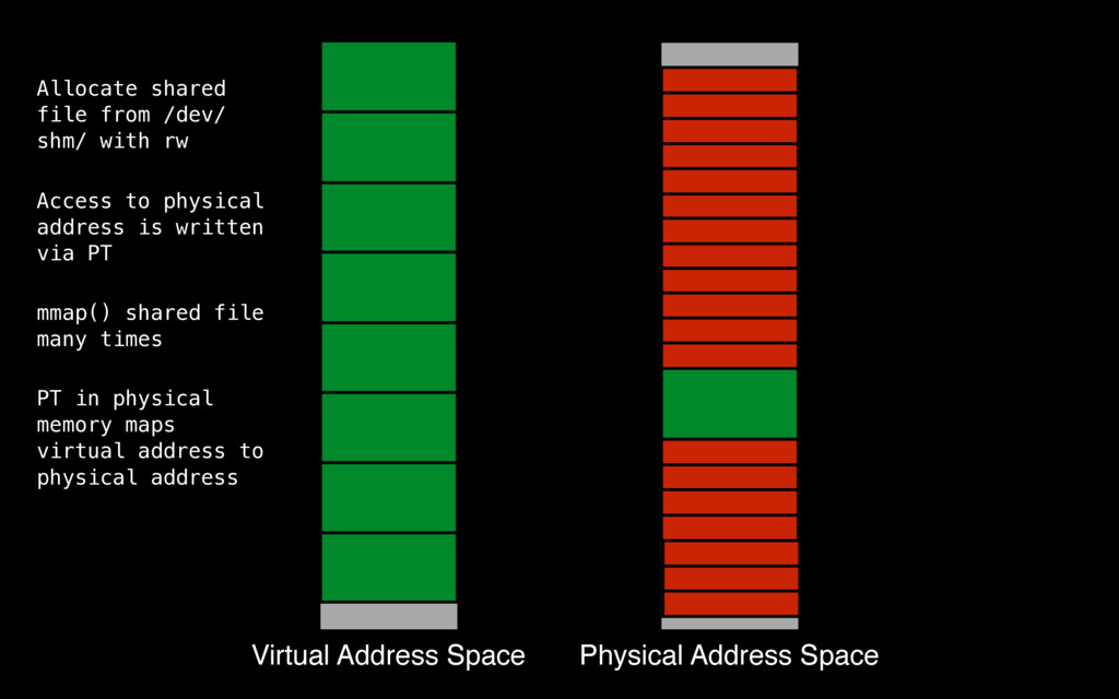
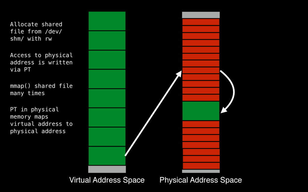
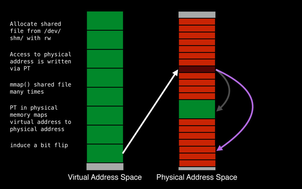
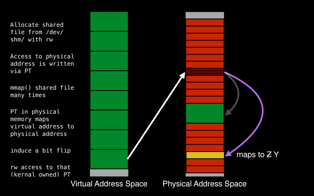
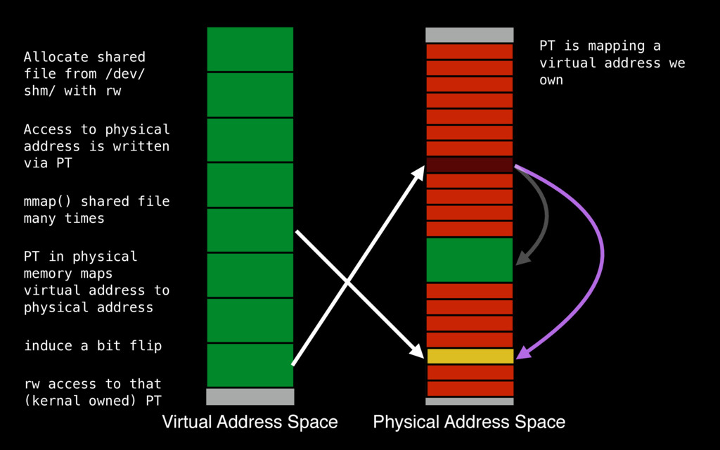
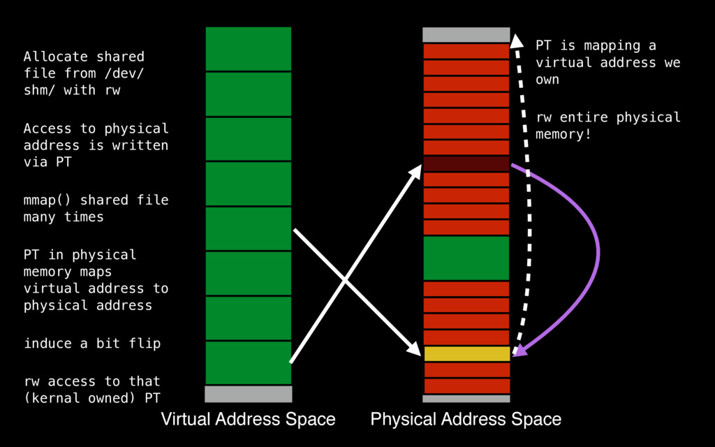
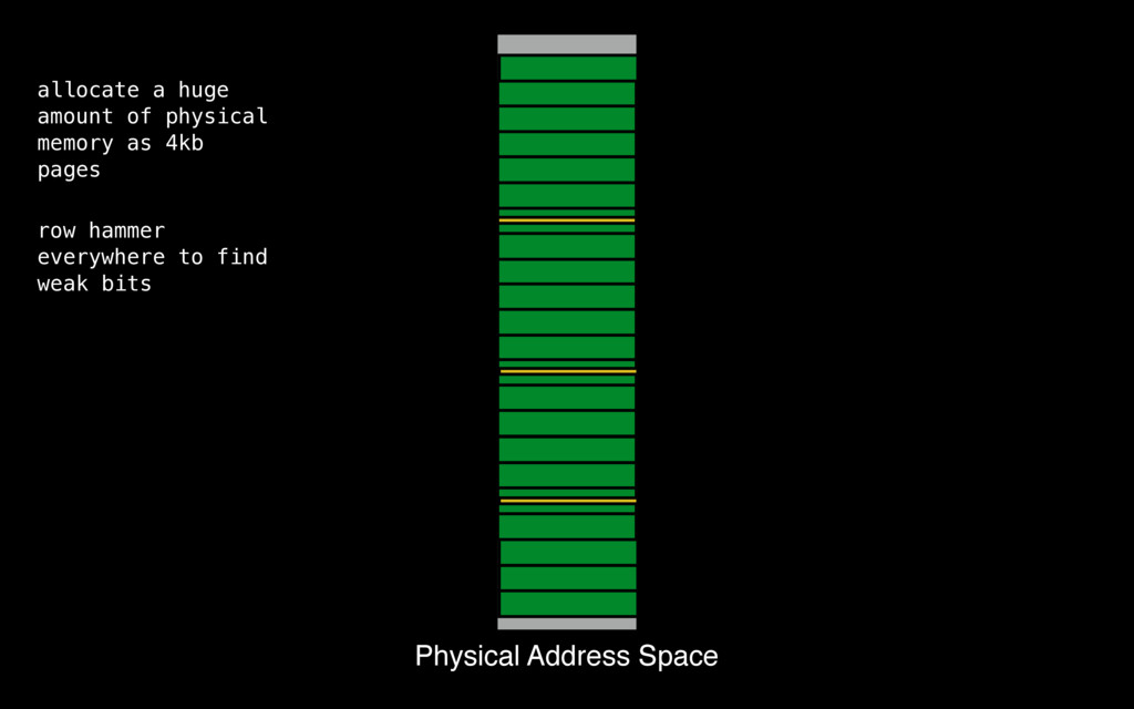
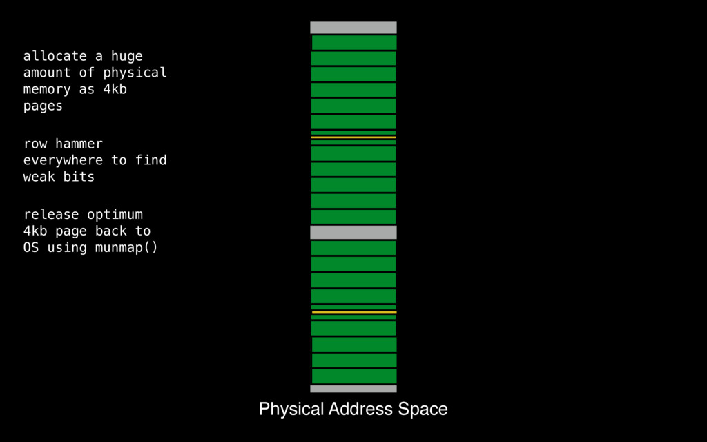
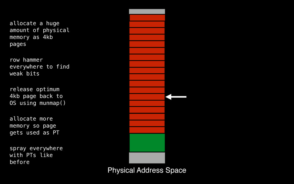
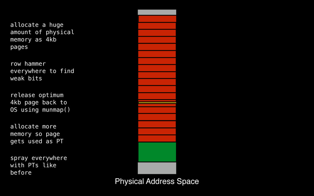
I gave a talk at Papers We Love Singapore about Row Hammer on March 6 2017. I spoke about how RAM works and how a simple capacitor charge leakage in modern DRAM can be turned into a privilege excalation attack.

Video link: https://engineers.sg/v/1447

Vishnu Prem

March 06, 2017
Tweet

More Decks by Vishnu Prem

Other Decks in Technology

Transcript

  1. Row Hammer:
    Flipping Bits in Memory Without
    Accessing Them
    Yoongu Kim
    Ross Daly
    Jeremie Kim
    Chris Fallin
    Ji Hye Lee
    Onur Mutlu
    Donghyuk Lee
    Chris Wilkerson
    Konrad Lai
    Papers We Love #026 | Vishnu Prem | @burnflare

    View Slide

  2. Hello!
    Vishnu Prem
    Y4 Computer Science @ NUS.
    NUS Hackers.
    This is my second Papers We Love.
    Presented Diffie-Hellman Key Exchange a year ago.

    View Slide

  3. The Paper
    Flipping Bits in Memory Without Accessing Them:
    An Experimental Study of DRAM Disturbance Errors
    Joint publication by CMU & Intel Labs.
    Hardware vulnerability in RAM that has
    security implications.
    Flaw is unpatchable

    View Slide

  4. What’s DRAM
    A trip down memory lane.

    View Slide

  5. Micron Technology MT4C1024 DRAM

    View Slide

  6. DRAM Cell
    Holds a single bit
    Implemented using Field-Effect
    Transistor & Capacitor
    Worldline activates, data dumped into
    bitline; C is discharged
    If C < Threshold =~ 0
    If C > Threshold =~ 1
    Loses its charge every 64ms
    wordline
    bitline
    FET
    C

    View Slide

  7. bit 1 case = 1V
    = 0V
    Step 0: Capacitor holds a charge
    wordline
    bitline

    View Slide

  8. bit 1 case = 1V
    = 0V
    Step 1: Precharge bitline to (1V - 0V) / 2 = 0.5V
    = 0.5V

    View Slide

  9. bit 1 case = 1V
    = 0V
    Step 2: Wordline raised to high V, transistor allows current to pass
    = 0.5V
    = High V

    View Slide

  10. bit 1 case = 1V
    = 0V
    Step 3: Since 1V > 0.5V, C is discharged onto bitline
    Increasing bitline slightly to 0.55V
    = 0.5V
    = High V
    Note: Charge is C is now
    destroyed

    View Slide

  11. bit 1 case = 1V
    = 0V
    Step 4: Sense Amplifiers detect slight change in bitline’s 0.55V = 1 bit
    They amplify bitline to 1V
    = 0.5V
    = High V

    View Slide

  12. bit 1 case = 1V
    = 0V
    Step 5: C is recharged (refreshed) back to 1V
    = 0.5V
    = High V

    View Slide

  13. bit 1 case = 1V
    = 0V
    Step 6: Wordline is switched off; bitline is switched off
    Value 1 read!
    = 0.5V
    = High V

    View Slide

  14. bit 0 case = 1V
    = 0V
    Step 0: Capacitor holds no charge

    View Slide

  15. bit 0 case = 1V
    = 0V
    Step 1: Precharge bitline to (1V - 0V) / 2 = 0.5V
    = 0.5V

    View Slide

  16. bit 0 case = 1V
    = 0V
    Step 2: Wordline raised to high V, transistor allows current to pass
    = 0.5V
    = High V

    View Slide

  17. bit 0 case = 1V
    = 0V
    Step 3: Since 0V < 0.5V, C is charged from bitline
    Decreasing bitline slightly to 0.45V
    = 0.5V
    = High V

    View Slide

  18. bit 0 case = 1V
    = 0V
    Step 4: Sense Amplifiers detect slight change in bitline’s 0.45V = 0 bit
    They amplify bitline to 0V
    = 0.5V
    = High V

    View Slide

  19. bit 0 case = 1V
    = 0V
    Step 5: C is discharged (refreshed) back to 0V
    = 0.5V
    = High V

    View Slide

  20. bit 0 case = 1V
    = 0V
    Step 6: Wordline is switched off; bitline is switched off
    Value 0 read!
    = 0.5V
    = High V

    View Slide

  21. Ok 1 bit is cool, many gigs how?

    View Slide

  22. View Slide

  23. View Slide

  24. Sen
    Sense
    Amplifiers

    View Slide

  25. wordline
    bitline
    FET
    C

    View Slide

  26. Row Selection
    Column Selection
    Row Buffer
    w
    b
    F
    C

    View Slide

  27. Row
    Colum
    Ro
    w
    b
    F
    C
    Row
    Colum
    Ro
    w
    b
    F
    C
    Row
    Colum
    Ro
    w
    b
    F
    C
    Row
    Colum
    Ro
    w
    b
    F
    C
    Row
    Colum
    Ro
    w
    b
    F
    C
    Row
    Colum
    Ro
    w
    b
    F
    C
    Row
    Colum
    Ro
    w
    b
    F
    C
    Row
    Colum
    Ro
    w
    b
    F
    C

    View Slide

  28. DRAM Array
    Row Selection
    Column Selection
    DRAM
    Controller
    Row Buffer

    View Slide

  29. DRAM Open Row
    0 1 1 0 1 0 0 1
    0 1 1 0 1 1 0 0
    0 1 1 0 1 1 1 1
    0 1 1 1 0 1 1 0
    0 1 1 0 0 1 0 1
    0 1 1 1 1 0 0 1
    0 1 1 0 1 1 1 1
    0 1 1 1 0 1 0 1
    Row Selection
    Column Selection
    DRAM
    Controller
    Row Buffer
    “Read Row 3, Col 4”

    View Slide

  30. DRAM Open Row
    0 1 1 0 1 0 0 1
    0 1 1 0 1 1 0 0
    0 1 1 0 1 1 1 1
    0 1 1 1 0 1 1 0
    0 1 1 0 0 1 0 1
    0 1 1 1 1 0 0 1
    0 1 1 0 1 1 1 1
    0 1 1 1 0 1 0 1
    Row Selection
    Column Selection
    DRAM
    Controller
    Row Buffer
    “Read Row 3, Col 4”
    1. bitlines charged
    2. wordline activated

    View Slide

  31. DRAM Open Row
    0 1 1 0 1 0 0 1
    0 1 1 0 1 1 0 0
    0 1 1 0 1 1 1 1
    0 1 1 0 0 1 0 1
    0 1 1 1 1 0 0 1
    0 1 1 0 1 1 1 1
    0 1 1 1 0 1 0 1
    0 1 1 1 0 1 1 0
    Row Selection
    Column Selection
    DRAM
    Controller
    Row Buffer
    “Read Row 3, Col 4”
    1. bitlines charged
    2. wordline activated
    3. cells discharge
    4. sense amps read bit

    View Slide

  32. DRAM Open Row
    0 1 1 0 1 0 0 1
    0 1 1 0 1 1 0 0
    0 1 1 0 1 1 1 1
    0 1 1 1 0 1 1 0
    0 1 1 0 0 1 0 1
    0 1 1 1 1 0 0 1
    0 1 1 0 1 1 1 1
    0 1 1 1 0 1 0 1
    0 1 1 1 0 1 1 0
    Row Selection
    Column Selection
    DRAM
    Controller
    Row Buffer
    “Read Row 3, Col 4” 1. bitlines charged
    2. wordline activated
    3. cells discharge
    4. sense amps read bit
    5. sense amps amplify
    6. row recharged

    View Slide

  33. DRAM Open Row
    0 1 1 0 1 0 0 1
    0 1 1 0 1 1 0 0
    0 1 1 0 1 1 1 1
    0 1 1 1 0 1 1 0
    0 1 1 0 0 1 0 1
    0 1 1 1 1 0 0 1
    0 1 1 0 1 1 1 1
    0 1 1 1 0 1 0 1
    0 1 1 1 0 1 1 0
    Row Selection
    Column Selection
    DRAM
    Controller
    Row Buffer
    “Read Row 3, Col 4”
    1. bitlines charged
    2. wordline activated
    3. cells discharge
    4. sense amps read bit
    5. sense amps amplify
    6. row recharged
    7. all 8 bits known!

    View Slide

  34. DRAM Open Row
    0 1 1 0 1 0 0 1
    0 1 1 0 1 1 0 0
    0 1 1 0 1 1 1 1
    0 1 1 1 0 1 1 0
    0 1 1 0 0 1 0 1
    0 1 1 1 1 0 0 1
    0 1 1 0 1 1 1 1
    0 1 1 1 0 1 0 1
    0 1 1 1 0 1 1 0
    Row Selection
    Column Selection
    DRAM
    Controller
    Row Buffer
    “Read Row 3, Col 4”
    1. bitlines charged
    2. wordline activated
    3. cells discharge
    4. sense amps read bit
    5. sense amps amplify
    6. row recharged
    7. all 8 bits known!
    “Read Row 3, Col 6”

    View Slide

  35. DRAM Write Cell
    0 1 1 0 1 0 0 1
    0 1 1 0 1 1 0 0
    0 1 1 0 1 1 1 1
    0 1 1 1 0 1 1 0
    0 1 1 0 0 1 0 1
    0 1 1 1 1 0 0 1
    0 1 1 0 1 1 1 1
    0 1 1 1 0 1 0 1
    0 1 1 1 0 1 1 0
    Row Selection
    Column Selection
    DRAM
    Controller
    Row Buffer
    “Write 0 on that cell”

    View Slide

  36. DRAM Write Cell
    0 1 1 0 1 0 0 1
    0 1 1 0 1 1 0 0
    0 1 1 0 1 1 1 1
    0 1 1 1 0 1 1 0
    0 1 1 0 0 1 0 1
    0 1 1 1 1 0 0 1
    0 1 1 0 1 1 1 1
    0 1 1 1 0 1 0 1
    0 1 1 1 0 1 0 0
    Row Selection
    Column Selection
    DRAM
    Controller
    Row Buffer
    “Write 0 on that cell”
    1. write 0 on col buffer

    View Slide

  37. DRAM Write Cell
    0 1 1 0 1 0 0 1
    0 1 1 0 1 1 0 0
    0 1 1 0 1 1 1 1
    0 1 1 1 0 1 1 0
    0 1 1 0 0 1 0 1
    0 1 1 1 1 0 0 1
    0 1 1 0 1 1 1 1
    0 1 1 1 0 1 0 1
    0 1 1 1 0 1 0 0
    Row Selection
    Column Selection
    DRAM
    Controller
    Row Buffer
    “Write 0 on that cell”
    1. write 0 on col buffer
    2. bitline set to 0V

    View Slide

  38. DRAM Write Cell
    0 1 1 0 1 0 0 1
    0 1 1 0 1 1 0 0
    0 1 1 0 1 1 1 1
    0 1 1 1 0 1 0 0
    0 1 1 0 0 1 0 1
    0 1 1 1 1 0 0 1
    0 1 1 0 1 1 1 1
    0 1 1 1 0 1 0 1
    0 1 1 1 0 1 0 0
    Row Selection
    Column Selection
    DRAM
    Controller
    Row Buffer
    “Write 0 on that cell”
    1. write 0 on col buffer
    2. bitline set to 0V
    3. 0 propogates to cell

    View Slide

  39. DRAM Close Row
    0 1 1 0 1 0 0 1
    0 1 1 0 1 1 0 0
    0 1 1 0 1 1 1 1
    0 1 1 1 0 1 0 0
    0 1 1 0 0 1 0 1
    0 1 1 1 1 0 0 1
    0 1 1 0 1 1 1 1
    0 1 1 1 0 1 0 1
    0 1 1 1 0 1 0 0
    Row Selection
    Column Selection
    DRAM
    Controller
    Row Buffer
    “Read another row”

    View Slide

  40. DRAM Close Row
    0 1 1 0 1 0 0 1
    0 1 1 0 1 1 0 0
    0 1 1 0 1 1 1 1
    0 1 1 1 0 1 0 0
    0 1 1 0 0 1 0 1
    0 1 1 1 1 0 0 1
    0 1 1 0 1 1 1 1
    0 1 1 1 0 1 0 1
    0 1 1 1 0 1 0 0
    Row Selection
    Column Selection
    DRAM
    Controller
    Row Buffer
    “Read another row”
    1. deactivate wordline
    2. discharge hotline

    View Slide

  41. DRAM Close Row
    0 1 1 0 1 0 0 1
    0 1 1 0 1 1 0 0
    0 1 1 0 1 1 1 1
    0 1 1 1 0 1 0 0
    0 1 1 0 0 1 0 1
    0 1 1 1 1 0 0 1
    0 1 1 0 1 1 1 1
    0 1 1 1 0 1 0 1
    Row Selection
    Column Selection
    DRAM
    Controller
    Row Buffer
    “Read another row”
    1. deactivate wordline
    2. discharge hotline
    3. row buffer cleared

    View Slide

  42. DRAM Refreshing
    0 1 1 0 1 0 0 1
    0 1 1 0 1 1 0 0
    0 1 1 0 1 1 1 1
    0 1 1 1 0 1 1 0
    0 1 1 0 0 1 0 1
    0 1 1 1 1 0 0 1
    0 1 1 0 1 1 1 1
    0 1 1 1 0 1 0 1
    Row Selection
    Column Selection
    DRAM
    Controller
    Row Buffer
    Capacitors lose their
    charge constantly
    DDR3: every cell will
    be refreshed every
    64ms
    Refresh = exactly
    same action as
    reading a row

    View Slide

  43. DRAM Refreshing
    0 1 1 0 1 0 0 1
    0 1 1 0 1 1 0 0
    0 1 1 0 1 1 1 1
    0 1 1 1 0 1 1 0
    0 1 1 0 0 1 0 1
    0 1 1 1 1 0 0 1
    0 1 1 0 1 1 1 1
    0 1 1 1 0 1 0 1
    Row Selection
    Column Selection
    DRAM
    Controller
    Row Buffer
    Capacitors lose their
    charge constantly
    DDR3: every cell will
    be refreshed every
    64ms
    Refresh = exactly
    same action as
    reading a row

    View Slide

  44. DRAM Refreshing
    0 1 1 0 1 0 0 1
    0 1 1 0 1 1 0 0
    0 1 1 0 1 1 1 1
    0 1 1 1 0 1 1 0
    0 1 1 0 0 1 0 1
    0 1 1 1 1 0 0 1
    0 1 1 0 1 1 1 1
    0 1 1 1 0 1 0 1
    Row Selection
    Column Selection
    DRAM
    Controller
    Row Buffer
    Capacitors lose their
    charge constantly
    DDR3: every cell will
    be refreshed every
    64ms
    Refresh = exactly
    same action as
    reading a row

    View Slide

  45. DRAM Refreshing
    0 1 1 0 1 1 0 0
    0 1 1 0 1 1 1 1
    0 1 1 1 0 1 1 0
    0 1 1 0 0 1 0 1
    0 1 1 1 1 0 0 1
    0 1 1 0 1 1 1 1
    0 1 1 1 0 1 0 1
    0 1 1 0 1 0 0 1
    Row Selection
    Column Selection
    DRAM
    Controller
    Row Buffer
    Capacitors lose their
    charge constantly
    DDR3: every cell will
    be refreshed every
    64ms
    Refresh = exactly
    same action as
    reading a row

    View Slide

  46. DRAM Refreshing
    0 1 1 0 1 0 0 1
    0 1 1 0 1 1 0 0
    0 1 1 0 1 1 1 1
    0 1 1 1 0 1 1 0
    0 1 1 0 0 1 0 1
    0 1 1 1 1 0 0 1
    0 1 1 0 1 1 1 1
    0 1 1 1 0 1 0 1
    Row Selection
    Column Selection
    DRAM
    Controller
    Row Buffer
    Capacitors lose their
    charge constantly
    DDR3: every cell will
    be refreshed every
    64ms
    Refresh = exactly
    same action as
    reading a row

    View Slide

  47. DRAM Key Takeaways
    Reading one bit requires entire row to
    be read & refreshed
    Every 64ms, every cell must be
    refreshed
    wordline
    bitline
    FET
    C

    View Slide

  48. DRAM Disturbances
    A tale of 0s & 1s.

    View Slide

  49. DRAM Disturbances
    Smaller, Faster, Cheaper
    Harder for manufacturers to electrical
    seal cells between each other
    Paper discovered sometimes this
    extreme compactness causes
    leakage in the cells

    View Slide

  50. View Slide

  51. View Slide

  52. ~1.2M accesses per refresh

    View Slide

  53. Row Hammer

    View Slide

  54. Row Hammer in Code
    code1a:
    mov (X), %eax
    mov (Y), %ebx
    clflush (X)
    clflush (Y)
    jmp code1a
    1
    2
    3
    4
    5
    6
    1
    2
    3
    4
    5
    6
    code1b:
    mov (X), %eax
    clflush (X)
    jmp code1a
    Experiment Control

    View Slide

  55. View Slide

  56. Row Hammer in Code
    0 0 0 0 0 0 0 0
    0 0 0 0 0 0 0 0
    0 0 0 0 0 0 0 0
    0 0 0 0 0 0 0 0
    0 0 0 0 0 0 0 0
    0 0 0 0 0 0 0 0
    0 0 0 0 0 0 0 0
    0 0 0 0 0 0 0 0
    Row Selection
    Column Selection
    DRAM
    Controller
    Row Buffer
    code1b:
    mov (X), %eax
    clflush (X)
    jmp code1a
    1
    2
    3
    4
    5
    6
    X

    View Slide

  57. Row Hammer in Code
    0 0 0 0 0 0 0 0
    0 0 0 0 0 0 0 0
    0 0 0 0 0 0 0 0
    0 0 0 0 0 0 0 0
    0 0 0 0 0 0 0 0
    0 0 0 0 0 0 0 0
    0 0 0 0 0 0 0 0
    0 0 0 0 0 0 0 0
    Row Selection
    Column Selection
    DRAM
    Controller
    Row Buffer
    code1b:
    mov (X), %eax
    clflush (X)
    jmp code1a
    1
    2
    3
    4
    5
    6
    X

    View Slide

  58. Row Hammer in Code
    0 0 0 0 0 0 0 0
    0 0 0 0 0 0 0 0
    0 0 0 0 0 0 0 0
    0 0 0 0 0 0 0 0
    0 0 0 0 0 0 0 0
    0 0 0 0 0 0 0 0
    0 0 0 0 0 0 0 0
    0 0 0 0 0 0 0 0
    0 0 0 0 0 0 0 0
    Row Selection
    Column Selection
    DRAM
    Controller
    Row Buffer
    code1b:
    mov (X), %eax
    clflush (X)
    jmp code1a
    1
    2
    3
    4
    5
    6
    X
    No flips

    View Slide

  59. Row Hammer in Code
    0 0 0 0 0 0 0 0
    0 0 0 0 0 0 0 0
    0 0 0 0 0 0 0 0
    0 0 0 0 0 0 0 0
    0 0 0 0 0 0 0 0
    0 0 0 0 0 0 0 0
    0 0 0 0 0 0 0 0
    0 0 0 0 0 0 0 0
    Row Selection
    Column Selection
    DRAM
    Controller
    Row Buffer
    code1a:
    mov (X), %eax
    mov (Y), %ebx
    clflush (X)
    clflush (Y)
    jmp code1a
    1
    2
    3
    4
    5
    6
    X
    Y

    View Slide

  60. Row Hammer in Code
    0 0 0 0 0 0 0 0
    0 0 0 0 0 0 0 0
    0 0 0 0 0 0 0 0
    0 0 0 0 0 0 0 0
    0 0 0 0 0 0 0 0
    0 0 0 0 0 0 0 0
    0 0 0 0 0 0 0 0
    0 0 0 0 0 0 0 0
    Row Selection
    Column Selection
    DRAM
    Controller
    Row Buffer
    code1a:
    mov (X), %eax
    mov (Y), %ebx
    clflush (X)
    clflush (Y)
    jmp code1a
    1
    2
    3
    4
    5
    6
    X
    Y
    Induces flips
    1
    1

    View Slide

  61. Row Hammer in Code
    code1a:
    mov (X), %eax
    mov (Y), %ebx
    clflush (X)
    clflush (Y)
    jmp code1a
    1
    2
    3
    4
    5
    6
    1
    2
    3
    4
    5
    6
    code1b:
    mov (X), %eax
    clflush (X)
    jmp code1a
    Induces errors No errors

    View Slide

  62. How do we pick the right X & Y?
    code1a:
    mov (X), %eax
    mov (Y), %ebx
    clflush (X)
    clflush (Y)
    jmp code1a
    0 0 0 0 0 0 0 0
    0 0 0 0 0 0 0 0
    0 0 0 0 0 0 0 0
    0 0 0 0 0 0 0 0
    0 0 0 0 0 0 0 0
    0 0 0 0 0 0 0 0
    0 0 0 0 0 0 0 0
    0 0 0 0 0 0 0 0
    Row Selection
    Column Selection
    DRAM
    Controller
    Row Buffer
    1
    2
    3
    4
    5
    6
    X
    Y

    View Slide

  63. Hammer: Memory Address Selection
    1. 8 banks -> 1/8 chance of same
    bank address pair
    2. Hammer 4 or 8 addresses at once
    3. Double-side row hammer
    Bare metal access Unprivileged access
    1. Get physical address from /proc/
    PID/pagemap

    View Slide

  64. View Slide

  65. View Slide

  66. 55ns activation
    ~ 1.1M activations / refersh
    64ms refresh
    ~ 1.1M activations / refersh

    View Slide

  67. Aggressor row vs. Victim row

    View Slide

  68. Try it at home! ***
    Iteration 0 (after 0.00s)
    Took 213.2 ms per address set
    Took 2.13183 sec in total for 10 address sets
    Took 49.348 nanosec per memory access (for 43200000 memory accesses)
    This gives 162114 accesses per address per 64 ms refresh period
    Checking for bit flips took 0.219196 sec

    View Slide

  69. Exploiting Row Hammer
    Cool stuff, Why should I be afraid?

    View Slide

  70. What’s Memory Protection?
    Unprotected vs. Protected Memory

    View Slide

  71. Unprotected Memory
    Physical Memory
    0x0000
    0xFFFF

    View Slide

  72. Unprotected Memory
    Physical Memory
    0x0000
    0xFFFF
    Process A

    View Slide

  73. Unprotected Memory
    Physical Memory
    0x0000
    0xFFFF
    Process A
    0x1111
    0x3333

    View Slide

  74. Unprotected Memory
    Physical Memory
    0x0000
    0xFFFF
    Process A
    Process B
    0x1111
    0x3333

    View Slide

  75. Unprotected Memory
    Physical Memory
    0x0000
    0xFFFF
    Process A
    Process B
    0x1111
    0x3333
    0x4444
    0x9999

    View Slide

  76. Unprotected Memory
    Physical Memory
    0x0000
    0xFFFF
    Process A
    Process B
    0x1111
    0x3333
    0x4444
    0x9999

    View Slide

  77. Unprotected Memory
    Physical Memory
    0x0000
    0xFFFF
    Process A
    Process B
    0x1111
    0x3333
    0x4444
    0x9999
    X

    View Slide

  78. Protected Memory
    Physical Memory
    0x0000
    0xFFFF

    View Slide

  79. Protected Memory
    Physical Memory
    0x0000
    0xFFFF
    Process A’s Virtual Memory
    0x0000
    0xFFFF

    View Slide

  80. Protected Memory
    Physical Memory
    0x0000
    0xFFFF
    Process A’s Virtual Memory
    0x0000
    0xFFFF

    View Slide

  81. Protected Memory
    Physical Memory
    0x0000
    0xFFFF
    Process A’s Virtual Memory
    0x0000
    0xFFFF

    View Slide

  82. Protected Memory
    Physical Memory
    0x0000
    0xFFFF
    Process A’s Virtual Memory
    0x0000
    0xFFFF
    Process B’s Virtual Memory
    0x0000
    0xFFFF

    View Slide

  83. Linux Page Tables
    A Page is a fixed length continuous
    block of memory. A page is usually 4k.
    Page Table stores mapping between
    virtual & physical addresses. PT is 4k.
    Each mapping in Page Table is a
    Page Table Entry (PTE). Up to 512
    PTEs in a PT.
    512 x 4kb = 2MB.
    Every 2MB of VM requires 4kb of PT
    space
    Physical Memory Virtual Memory

    View Slide

  84. Virtual Address Space Physical Address Space

    View Slide

  85. Virtual Address Space Physical Address Space
    Allocate shared
    file from /dev/
    shm/ with rw

    View Slide

  86. Virtual Address Space Physical Address Space
    Allocate shared
    file from /dev/
    shm/ with rw
    Access to physical
    address is written
    via PT

    View Slide

  87. Virtual Address Space Physical Address Space
    Allocate shared
    file from /dev/
    shm/ with rw
    Access to physical
    address is written
    via PT
    mmap() shared file
    many times

    View Slide

  88. Virtual Address Space Physical Address Space
    Allocate shared
    file from /dev/
    shm/ with rw
    Access to physical
    address is written
    via PT
    mmap() shared file
    many times
    PT in physical
    memory maps
    virtual address to
    physical address

    View Slide

  89. Virtual Address Space Physical Address Space
    Allocate shared
    file from /dev/
    shm/ with rw
    Access to physical
    address is written
    via PT
    mmap() shared file
    many times
    PT in physical
    memory maps
    virtual address to
    physical address

    View Slide

  90. Virtual Address Space Physical Address Space
    Allocate shared
    file from /dev/
    shm/ with rw
    Access to physical
    address is written
    via PT
    mmap() shared file
    many times
    PT in physical
    memory maps
    virtual address to
    physical address
    induce a bit flip

    View Slide

  91. x86-64 Page Table Entries
    Page Table contains array of 512 PTEs
    Each PTE is 64bit, looks like this:
    20 bits on 4GB system → 31% chance

    View Slide

  92. Virtual Address Space Physical Address Space
    Allocate shared
    file from /dev/
    shm/ with rw
    Access to physical
    address is written
    via PT
    mmap() shared file
    many times
    PT in physical
    memory maps
    virtual address to
    physical address
    induce a bit flip

    View Slide

  93. Virtual Address Space Physical Address Space
    Allocate shared
    file from /dev/
    shm/ with rw
    Access to physical
    address is written
    via PT
    mmap() shared file
    many times
    PT in physical
    memory maps
    virtual address to
    physical address
    induce a bit flip
    rw access to that
    (kernal owned) PT
    maps to Z Y

    View Slide

  94. PT is mapping a
    virtual address we
    own
    Virtual Address Space Physical Address Space
    Allocate shared
    file from /dev/
    shm/ with rw
    Access to physical
    address is written
    via PT
    mmap() shared file
    many times
    PT in physical
    memory maps
    virtual address to
    physical address
    induce a bit flip
    rw access to that
    (kernal owned) PT

    View Slide

  95. PT is mapping a
    virtual address we
    own
    rw entire physical
    memory!
    Virtual Address Space Physical Address Space
    Allocate shared
    file from /dev/
    shm/ with rw
    Access to physical
    address is written
    via PT
    mmap() shared file
    many times
    PT in physical
    memory maps
    virtual address to
    physical address
    induce a bit flip
    rw access to that
    (kernal owned) PT

    View Slide

  96. Exploiting Write Access to PTE
    Modify SUID (Set User ID upon execution) executables such as /bin/ping
    Overwriting entry point to run shell code
    Our shell code now runs as root!

    View Slide

  97. Page Reuse
    Previous exploit requires us to be lucky
    We can increase our chances using PT reuse and create our own luck
    We know weak cells in a particular DRAM are repeatable

    View Slide

  98. Physical Address Space
    allocate a huge
    amount of physical
    memory as 4kb
    pages

    View Slide

  99. Physical Address Space
    allocate a huge
    amount of physical
    memory as 4kb
    pages
    row hammer
    everywhere to find
    weak bits

    View Slide

  100. Physical Address Space
    allocate a huge
    amount of physical
    memory as 4kb
    pages
    row hammer
    everywhere to find
    weak bits
    release optimum
    4kb page back to
    OS using munmap()

    View Slide

  101. Physical Address Space
    allocate a huge
    amount of physical
    memory as 4kb
    pages
    row hammer
    everywhere to find
    weak bits
    release optimum
    4kb page back to
    OS using munmap()
    allocate more
    memory so page
    gets used as PT

    View Slide

  102. Physical Address Space
    allocate a huge
    amount of physical
    memory as 4kb
    pages
    row hammer
    everywhere to find
    weak bits
    release optimum
    4kb page back to
    OS using munmap()
    allocate more
    memory so page
    gets used as PT
    spray everywhere
    with PTs like
    before

    View Slide

  103. Physical Address Space
    allocate a huge
    amount of physical
    memory as 4kb
    pages
    row hammer
    everywhere to find
    weak bits
    release optimum
    4kb page back to
    OS using munmap()
    allocate more
    memory so page
    gets used as PT
    spray everywhere
    with PTs like
    before

    View Slide

  104. bitflip target bit
    via row hammer
    Physical Address Space
    allocate a huge
    amount of physical
    memory as 4kb
    pages
    row hammer
    everywhere to find
    weak bits
    release optimum
    4kb page back to
    OS using munmap()
    allocate more
    memory so page
    gets used as PT
    spray everywhere
    with PTs like
    before

    View Slide

  105. bitflip target bit
    via row hammer
    rw entire physical
    memory!
    Physical Address Space
    allocate a huge
    amount of physical
    memory as 4kb
    pages
    row hammer
    everywhere to find
    weak bits
    release optimum
    4kb page back to
    OS using munmap()
    allocate more
    memory so page
    gets used as PT
    spray everywhere
    with PTs like
    before

    View Slide

  106. More Row Hammer Exploits
    NaCl - Google Native Client
    Flip Feng Shui - Compromise OpenSSH & apt-get
    Drammer - Android POC

    View Slide

  107. Mitigations
    Stopping this.

    View Slide

  108. View Slide

  109. Solutions Proposed
    Make better chips
    Self correction (ECC DRAM)
    Increase refresh rate
    Targeted row refresh
    Probabilistic Adjacent Row Activation

    View Slide

  110. Targeted Row Refresh
    Identify “hot” rows and refresh neighbours
    Count activations for a row
    Refresh neighbours when counter reaches threshold
    LPDDR4 has this in spec

    View Slide

  111. Probabilistic Adjacent Row Activation
    Proposal in the paper
    Every time a row is opened or closed, refresh an adjacent row with very low
    probability
    Statistically, adjacent rows will be refreshed if one row is hammered

    View Slide

  112. References & Links
    Thank you!
    The paper
    Google Project Zero blogpost
    Blackhat presentation
    Drammer Android POC

    View Slide

  113. Row Hammer:
    Flipping Bits in Memory Without
    Accessing Them
    Yoongu Kim
    Ross Daly
    Jeremie Kim
    Chris Fallin
    Ji Hye Lee
    Onur Mutlu
    Donghyuk Lee
    Chris Wilkerson
    Konrad Lai
    Papers We Love #026 | Vishnu Prem | @burnflare

    View Slide