Upgrade to Pro — share decks privately, control downloads, hide ads and more …

CVIM_2022_01

KK
February 27, 2022

 CVIM_2022_01

Computational imaging based on multi-tap CMOS image sensors and multi-aperture optics

KK

February 27, 2022
Tweet

Other Decks in Research

Transcript

  1. Computational imaging based on multi- tap CMOS image sensors and

    multi- aperture optics Keiichiro Kagawa Research Institute of Electronics, Shizuoka University
  2.  B.Eng. & M.Eng. degrees from Osaka University, Japan, in

    1996 and 1998, respectively  Ph.D. degree from Osaka University, Japan, in 2001  Was with Nara Institute of Science and Technology, Japan, 2001-2007  Was with Osaka University, Japan, 2007-2011  Have been with Shizuoka University, Japan, since 2011  My interests are in applications and development of CMOS image sensors for biomedical imaging and computational imaging  Email: [email protected] Self Introduction
  3. Outline  Low-level processing in the charge domain ◼ Compressive

    sensing ◼ Multi-tap CMOS pixels  Ultra-high-speed filming ◼ Single-shot ◼ Multi-exposure for time-of-flight range imaging
  4. Contemporary CMOS image sensor CMOS VLSI analog/digital circuits CCD’s legacy

    pinned photodiode + High performance Gain amplifier ADC High frame rate High pixel count High photosensitivity Low noise Low dark current
  5. How to Implement Functions in Camera Systems Ordinary pixel array

    + Rich digital signal processing circuits Pixel array with in-pixel rich processing circuits Low-level focal-plane processing without in- pixel circuits Simple and small pixel Complicated and large pixel Post-processing Reduced data Results Results Results Conventional Charge-domain signal processing Smart pixel
  6.  Position: x, y, z  Direction: kx, ky, kz

     Time: t  Wavelength: λ  Polarization: S0 , S1 , S2 , S3 (Stokes parameters)  … Compression of Optical Signals
  7. Compressive Sensing (CS) More sampling points are reproduced from less

    samplings a Observation matrix Measured signal Original signal b (K-sparse)
  8. Mathematical Formulation a b (K-sparse) Observation matrix Measured signal Original

    signal min𝑥 = ෍ 𝑖 𝐷𝑖 𝒙 1 1, s. t. 𝐴𝒙 = 𝒚 min𝑥 = ෍ 𝑖 𝐷𝑖 𝒙 1 1 + 1 2 𝐴𝒙 − 𝒚 2 2, s. t. 𝐴𝒙 = 𝒚 Total variation (TV) is used
  9. Fundamental Operation: Inner Product Operation a Observation matrix Measured signal

    Original signal 𝑦𝑖 = 𝒂𝑖 ∙ 𝒙 Inner product (or correlation) b (K-sparse)
  10.  Single-pixel imaging Single detector  Compressive video Narrower bandwidth

     Hyper-spectrum camera A lot of wavelength spectral bands  Lensless camera Ultra-thin  X-ray CT Lower X-ray exposure or shorter acquisition time  … Examples of CS applications
  11. 4T active pixel  Pinned photodiode (Buried and fully depleted)

     Complete charge transfer  Floating diffusion amplifier  Low dark current  Noiseless charge handling  High conversion gain p n n + Depletion region p + SiO2
  12. Charge Modulators Sort Drain + = Used in time-of-flight depth

    image sensors and computational image sensors Temporal shutter a Time x a
  13. Inner Product Operation by Charge Modulators Sort Drain + =

    Temporal shutter a Time x a 𝑦𝑖 = 𝒂𝑖 ∙ 𝒙 Temporal inner product (or correlation)
  14.  Noiseless operation ◼ By complete charge transfer with pinned

    photo diodes  No processing circuit is necessary ◼ Low-level signal processing is done in the charge domain Benefits of Charge Modulators
  15. Related Work: Compressive Video [Hitomi et al. (2011)] [Sonoda et

    al. (2016)] Add the address line +High sensitivity High resolution - Temporal constraint Share the control line +High sensitivity High resolution -Spatial constraint [Luo et al. (2019)] In-pixel shutter memory +No constraint -Lower sensitivity Lower resolution
  16. Ultra-High-Speed Image Sensors Crack propagation Shock-wave propagation Plasma emission Crash

    test Continuous readout Burst readout Frame rate 1kfps 10kfps 10Mfps 100Mfps 1Gfps 20Mfps 16.7Mfps For example 3.5kfps High-speed ADC Column memory CMOS In-pixel memory CCD In-pixel memory CMOS Our method: in-pixel CS CMOS 303Mfps 125Mfps
  17. Bottleneck: In-Pixel Memory CCD Multi-stage charge transfer - High gate

    voltages for high transfer efficiency - High power consumption Bottleneck
  18. Bottleneck: Column Memory CMOS Long shared readout line - Parasitic

    resistance and capacitance Bottleneck High current density - Electromigration
  19.  DO NOT use analog amplification circuits  To reduce

    the number of memory elements operated at the same time Key to Realize Ultra-Fast Frame Rates
  20. Our Work: Multi-Aperture and Macro-Pixel CS Multi-aperture Macro pixel Shutter

    pattern Per aperture Per subpixel Disparity Yes No Lens Special lens array Ordinary lenses Macro pixel Subpixels Apertures
  21. Architecture Comparison Pixel array Multi-frame buffer Conventional Output Readout PD

    CDS Memory Pixel Focal-plane shutter controller Our multi-aperture CS Pixel array Pixel array Pixel array Output Readout Sub image sensors Post-processing
  22. Comparison of Time-Window Functions Multi-aperture framing A1 A2 A3 A4

    Observation period Multi-aperture compressive A1 A2 A3 A4 Observation period Conventional burst readout Observation period F1 F2 F3 F4 Time Efficient sampling
  23.  Only the speed of one-step charge transfer determines the

    maximum frame rate.  More frames or extended depth range is obtained in single-shot filming and time-of-flight depth imaging, respectively. Benefits of CS in Ultra-High-Speed Filming
  24. Compressive Sensing (CS) More sampling points are reproduced from less

    samplings. a Observation matrix Measured signal Original signal b (K-sparse)
  25. Multi-Aperture CS a apertures b frames (sparse with TV) =

    x A y Observation matrix Measured signal Original signal Time Time
  26. Comparison Pixel array Multi-frame buffer Noise reduction & Signal transfer

    causes a pause ↓ Limited frame rate Conventional Single-aperture Output Readout Multi-aperture CS Solving an inverse problem Focal plane time-coded multiple exposure Multi-aperture Pixel array Pixel array Pixel array Output Pixel array itself works as a frame buffer No pause Higher frame rate Noise reduction & readout
  27. Considerations on pixel design  No barriers and dips 

    Fringing electric field p n n + SiO 2 n+ Fringing electric field Depth p n n + Depletion region p + SiO 2 Dip Barrier Diffusion Drift
  28. Examples of Multi-tap LEFMs  Multiple charge storage diodes per

    pixel  Low noise by true CDS  High-speed charge modulation
  29. 200Mfps Multi-Aperture CS Camera SPI Vertical scanner LVDS AP controller

    PLL Clock tree Bias circuit OB 5×3 APs Read circuit 5x3 lens array
  30. Demonstration of single-shot UHS video capturing Focused laser beam Air

    break down plasma Camera APD Stop trigger FPGA CAPTURE_START • 15 apertures • 32-bit shutter pattern • 200Mfps capturing • Capturing is stopped by “Stop trigger”
  31. Results (Single shot) Compressed 15 images Time resolved 32 images

    (comp. ratio ~ 47%) Chengbo Li, http://www.caam.rice.edu/~optimization/L1/TVAL3/ #18 Frame #12 5ns Time Applied shutter patterns Solving inverse problem by TVAL3 Ideal pattern Impulse response Minimum pulse width = Time resolution
  32. Our Macro-Pixel CS camera: 303Mfps Object Time Macropixel Convolution with

    spatial PSF Temporally compressed images Reproduced images PD 1 2 3 4 PD 1 2 3 4 PD 1 2 3 4 PD 1 2 3 4 * Temporal coded shutter Subpixel (SP)-1 SP-3 SP-2 SP-4 Tap Single-aperture imaging lens Temporally compressive CMOS image sensor Time
  33. Example of Temporal Coded Shutter Time Tap SP 1 2

    3 4 Bit 1 2 3 4 5 6 7 8 9 10 11 12 13 14 15 16 17 18 19 20 21 22 23 24 25 26 27 28 29 30 31 32 1 2 3 4 1 2 3 4 1 2 3 4 1 2 3 4 Macropixel PD 1 2 3 4 PD 1 2 3 4 PD 1 2 3 4 PD 1 2 3 4 Tap
  34. Simulation of compression and reproduction 32 original images Time Captured

    compressed images @compression ratio of 800% 32 reproduced images @PSNR=34.1dB
  35. PSF and shutters ISSCC 2022 - Forum X.Y: <Presentation Title>

    40 of 70 bit 1 2 3 4 5 6 7 8 9 10 11 12 13 14 15 16 17 18 19 20 21 22 23 24 25 26 27 28 29 30 31 32 sp1G1 sp1G2 sp1G3 sp1G4 sp2G1 sp2G2 sp2G3 sp2G4 sp3G1 sp3G2 sp3G3 sp3G4 sp4G1 sp4G2 sp4G3 sp4G4
  36. Sensor Architecture PLL Registers SPI-2 SPI-1 Shutter controller (SC) Charge

    modulator drivers Macropixel array Column amplifiers and A/D converters Readout circuit Capture start/end and shutter pattern readout controller Shutter pattern memory (8b×32×16ch) Shift register array (8b×16ch) Drain controller CLK FETCH ADR[4:0] 16b 8b×16ch GSP1[4:1], GSP2[4:1], GSP3[4:1], GSP4[4:1] 16b TRG RDY SYNC SHLN[5:0] ENDRN SHLN[5:0] ENDRN Vertical scanner Horizontal scanner Digital image output CLK CLK High-speed part
  37. Timing Chart for Single-Shot CLK TRG RDY SYNC ADR[4:0] FETCH

    GSP1[1] GSP2[2] End of capturing Cycle Start End 0 1 0 0 1st byte 2nd byte Standby Image capturing Standby
  38. Chip Microphotograph Macropixel array Shutter controller Charge modulator drivers SPI-2

    & registers Vertical scanner PLL Column amplifiers, A/D converters, readout circuit, and horizontal scanner
  39. Specifications Comparison This work ISSCC’15 MDPI Sensors MDPI Sensors ISSCC’12

    Technology 0.11μm CMOS FSI 0.11μm CMOS FSI 0.18μm CMOS FSI 0.13μm CMOS/CCD BSI 0.18μm CMOS FSI Chip size 7.0mmH× 9.3mmV 7.0mmH× 9.3mmV 4.8mmH× 4.8mmV - 15mmH× 24mmV (Macro)pixel size 22.4μmH× 22.4μmV 11.2μmH× 5.6μmV 70μmH×35μmV 12.73μmH×12.7 3μmV 32μmH× 32μmV Effective (sub)pixel count 212H×188V 320H×324V 50H×108V 576H×512V 400H×250V (Sub)pixel count per macro pixel/aperture 2H×2V 5H×3V - - - Tap count per (sub)pixel/aperture 4 1 + drain - - - Maximum shutter length 256b 128b - - - Number of frames in burst operation 12@1x, 32@2x 15@1x, 30@2x 368 (in-pixel), 184 (off-pixel) 10 248 Maximum burst frame rate 303Mfps 200Mfps 100Mfps (in-pixel), 125Mfps(off-pixel) 100Mfps 20Mfps Image readout frame rate 21fps 22fps N/A - 15kfps Power consumption 2.8W 1.62W N/A - 24W Multiple exposure Yes Yes No No No Compatibility with normal optics Yes No Yes Yes Yes
  40. Experimental Setup for Single-Shot Filming Microscope (5x) Microscope (5x) RGB

    camera Developed CMOS image sensor PD for stop trigger 10x objective lens Pulse laser (λ=1064nm) Specimen (SPCC) Plasma image by the RGB camera Motorized stage
  41. Shutter for Non-Compression bit 1 2 3 4 5 6

    7 8 9 10 11 12 1 2 3 4 5 6 sp1G1 sp1G2 sp1G3 sp1G4 sp2G1 sp2G2 sp2G3 sp2G4 sp3G1 sp3G2 sp3G3 sp3G4 sp4G1 sp4G2 sp4G3 sp4G4 Drain 3.29 ns
  42. Shutter for 2x Compression 3.29 ns bit 1 2 3

    4 5 6 7 8 9 101112131415161718192021 2 2 23242526272829303132 sp1G1 sp1G2 sp1G3 sp1G4 sp2G1 sp2G2 sp2G3 sp2G4 sp3G1 sp3G2 sp3G3 sp3G4 sp4G1 sp4G2 sp4G3 sp4G4
  43. Tap SP 3 4 1 2 3 4 1 2

    3 4 Measured Impulse Response: 2x Compression Tap SP 1 2 1 2 3 4 1 2 3 4
  44. Experimental Setup for Light Reflection Filming Pulsed laser (λ=660nm, pulse

    width of 7ns) Mirror Developed CMOS image sensor Aperture Light source and camera Captured scene Panel (13.0m) Doll (8.0m) Pylon (6.0m) Pillar (4.0m) Lens Diffuser
  45. Decomposing Dual Path in TOF Pulsed laser (660 nm) Developed

    camera Mirror Letters “SU” Weak diffuser 3.30 m Diffuser Letters
  46. One-Pass Image Reproduction with DNN Courtesy of Prof. Nagahara, Osaka

    Univ. Compressed image Reproduced images by DNN
  47. Motion Recognition from a Compressed Image 1/2 Courtesy of Prof.

    Nagahara, Osaka Univ. Scene Reconstructed video Decoder Reconstruction Action label Hand Waving CNN Action recognition Coded exposure image Capture
  48. Motion Recognition from a Compressed Image 2/2 Video Coded Covering

    something with something Moving something down Real Input Model Top 1 Top 3 Top 5 Video (upper bound) C3D 71.0 88.0 88.0 Single image Coded exposure (Proposed) SVC2D 72.0 84.0 88.0 Long exposure C2D 20.0 40.0 52.0 Short exposure C2D 21.0 47.0 60.0 Courtesy of Prof. Nagahara, Osaka Univ. Video Compressed Covering something with something Moving something down
  49.  Inner-product (or correlation) operation as low-level charge- domain signal

    processing is introduced to compress temporal optical signals.  Temporally compressive ultra-high-speed CMOS image sensor based on the inner-product operation has been fabricated.  Single-shot filming and multi-exposure-based transient imaging have been demonstrated at a burst frame rate of 303Mfps.  Extended depth range and separation of dual-path components have been demonstrated.  Applications of DNN such as one-path image reproduction and motion recognition from a compressed image were introduced. Summary
  50. References 1/2  (CS) E. J. Cades and M. B.

    Wakin, “An introduction to compressive sampling,” IEEE Signal Processing Magazine, Vol. 25, pp. 21-30 (2008).  (compressive video1) Y. Hitomi, J. Gu, M. Gupta, T. Mitsunaga, and S. K. Nayar, “Video from a single coded exposure photograph using a learned over-complete dictionary,” ICCV (2011).  (compressive video2) T. Sonoda, H. Nagahara, K. Endo, Y. Sugiyama, and R. Taniguchi, “High-speed imaging using CMOS image sensor with quasi pixel-wise exposure,” ICCP (2016).  (compressive video3) Y. Luo, J. Jiang, M. Cai, and S. Mirabbasi, “CMOS computational camera with a two-tap coded exposure image sensor for single-shot spatial-temporal compressive sensing,” Optics Express, Vol. 27, pp. 31475-31489 (2019).  (spatial CS) Y. Oike and A. E. Gamal, “A 256x256 CMOS image sensors with ΔΣ-based single-shot compressed sensing,” IEEE ISSCC Dig. Tech. Papers, pp. 386-387(2012).  (UHS1) T. Arai, J. Yonai, T. Hayashida, H. Ohtake, H. van Kujik, and T. G. Etoh, “A 252-V/lux・s, 16.7-million- frames-per-second 312-kpixel back-side-illuminated ultrahigh-speed charge-coupled device,” IEEE Electron Devices, Vol. 60, pp. 3450-3458(2013).  (UHS2) Y. Tochigi, et al., “A global-shutter CMOS image sensor with readout speed of 1Tpixel/s burst and 780Mpixel/s continuous,” ISSCC Dig. Tech. Papers, pp. 382-383 (2012).  (UHS3) M. Suzuki, et al., “Over 100 Million Frames per Second 368 Frames Global Shutter Burst CMOS Image Sensor with In-Pixel Trench Capacitor Memory Array,” Proc. IISW, pp. 266-269 (2019).  (UHS4) T. Etoh, T. Okinaka, Y. Takano, K. Takehara, H. Nakano, K. Shimonomura, T. Ando, N. Ngo, Y. Kamakura, V. Dao, A. Nguyen, E. Charbon, C. Zhang, P. Moor, P. Goeschalckx, and L. Haspeslagh, “Light-in- flight imaging by a silicon image sensor: toward the theoretical highest frame rate,” MDPI Sensors, Vol. 19, Article 2247 (2019).
  51. References 2/2  (LEFM1) S. Kawahito, G. Baek, Z. Li,

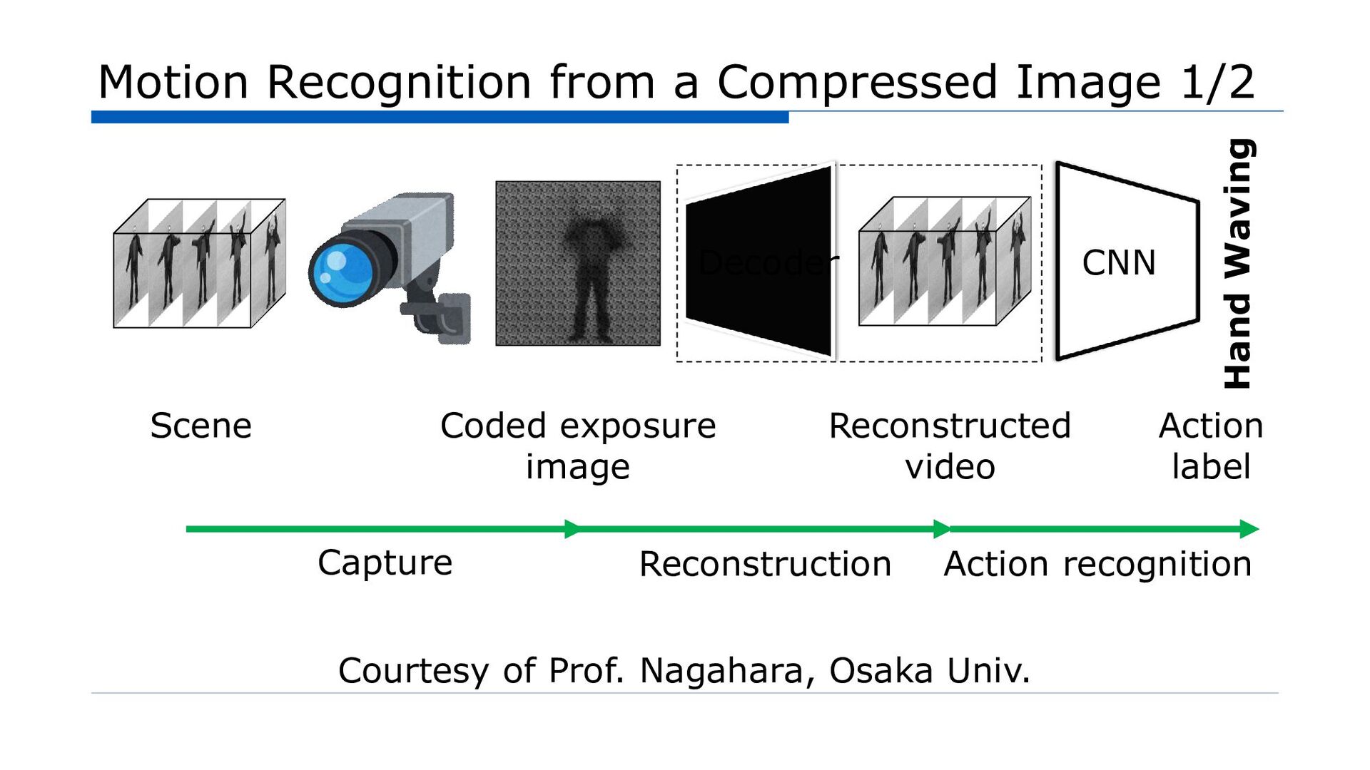
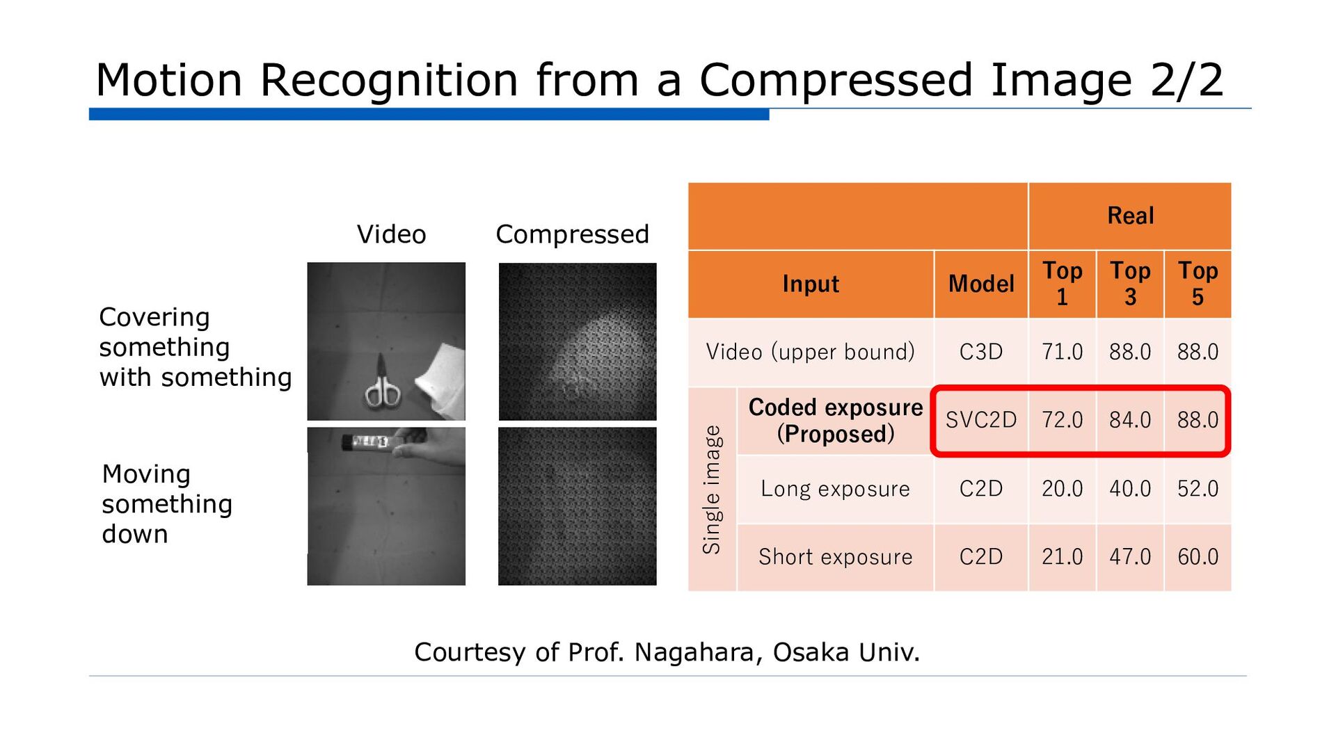
    S. Han, M. Seo, K. Yasutomi, and K. Kagawa, “CMOS lock-in pixel image sensors with lateral electric field control for time-resolved imaging,” Int'l Image Sensor Workshop, pp. 361-364 (2013).  (LEFM2) M. Seo, K. Kagawa, K. Yasutomi, T. Takasawa, Y. Kawata, N. Teranishi, Z. Li, I.A. Halin, and S. Kawahito, “10.8ps-time-resolution 256x512 image sensor with 2-tap true-CDS lock-in pixels for fluorescence lifetime imaging,” IEEE ISSCC Dig. Tech. Papers, pp. 198-199 (2015).  (LEFM3) M. Seo, Y. Shirakawa, Y. Masuda, Y. Kawata, K. Kagawa, K. Yasutomi, S. Kawahito, “A programmable sub-nanosecond time-gated 4-tap lock-in pixel CMOS image sensor for real-time fluorescence lifetime imaging microscopy,” ISSCC Dig. Tech. Papers, pp. 70-71 (2017).  (LEFM4) Y. Shirakawa, K. Yasutomi, K. Kagawa, S. Aoyama, and S. Kawahito, “An 8-tap CMOS lock-in pixel image sensor for short-pulse time-of-flight measurements,” MDPI Sensors, Vol. 20, Article 1040 (2020).  (Our work1) F. Mochizuki, K. Kagawa, S. Okihara, M. Seo, Z. Bo, T. Takasawa, K. Yasutomi, and S. Kawahito, “Single-shot 200Mfps 5x3-aperture compressive CMOS imager,” IEEE ISSCC Dig. Tech. Papers, pp. 116- 117(2015).  (Our work2) K. Kagawa, T. Kokado, Y. Sato, F. Mochizuki, H. Nagahara, T. Takasawa, K. Yasutomi, and S. Kawahito, “Multi-tap Macro-Pixel Based Compressive Ultra-High-Speed CMOS Image Sensor,” Proc. IISW, pp. 270-273 (2019).  (CS action recognition) T. Okawara, M. Yoshida, H. Nagahara, and Y. Yagi, “Action recognition from a single coded image,” ICCP (2020).  (DNN compressive video) M. Yoshida, A. Torii, M. Okutomi, K. Endo, Y. Sugiyama, R. Taniguchi, and H. Nagahara, “Joint optimization for compressive video sensing and reconstruction under hardware constraints,” ECCV (2018).