Upgrade to Pro — share decks privately, control downloads, hide ads and more …

Earth-abundant materials for next-generation photovoltaics

PaleBlueSam
November 28, 2019

Earth-abundant materials for next-generation photovoltaics

Energy Futures Lab seminar on new technologies being used in photovoltaics.

PaleBlueSam

November 28, 2019
Tweet

Other Decks in Science

Transcript

  1. Samantha Hood Computational design of earth-abundant thin film solar cells

    Materials Deign Group, Department of Materials @PaleBlueSam
  2. • Materials Design Group • Towards terawatt scale PV •

    STARCELL project • Predicting defect limited efficiencies • Emerging thin-film material: CZTS and Sb2 Se3 Outline Panda Solar Farm in Datong, China
  3. Materials Design Group Computational design of materials for clean energy:

    • Thin-film solar cells • Solar fuels • Batteries • Metal-organic frameworks http://wmd-group.github.io
  4. Our tools Multi-Scale Simulation Toolbox Density Functional Th Source: F.

    Bechstedt – Many-body Approac Hohenberg-Kohn (1964); Quantum Mechanics ˆ HΨ = EΨ Kinetic and Potential Energy Op ˆ H = ˆ T + ˆ V Non Relativistic Relativist Schrödinger (1887, Vienna) Dirac (1902, Bristo Extra terms scalar relativis spin-orbit coup Density Functional Theory (DFT) Source: F. Bechstedt – Many-body Approach to Electronic Excitations (2015) Hohenberg-Kohn (1964); Kohn-Sham (1965) Density Functional Theory (DFT) Many-body Approach to Electronic Excitations (2015 Hohenberg-Kohn (1964); Kohn-Sham (1965) Many-body perspective
  5. Materials Modelling with DFT Materials Modelling with DFT Input Chemical

    Structure or Composition Output Total Energy + Electronic Structure Structure atomic forces equilibrium coordinates atomic vibrations phonons elastic constants Thermodynamics internal energy (U) enthalpy (H) free energy (G) activation energies (ΔE) Electron Energies density of states band structure effective mass tensors electron distribution magnetism Excitations transition intensities absorption spectra dielectric functions spectroscopy https://speakerdeck.com/aronwalsh/from-atoms-to-devices-materials-design-for-new-energy-technologies?slide=61
  6. Materials Modelling with DFT Materials Modelling with DFT Input Chemical

    Structure or Composition Output Total Energy + Electronic Structure Structure atomic forces equilibrium coordinates atomic vibrations phonons elastic constants Thermodynamics internal energy (U) enthalpy (H) free energy (G) activation energies (ΔE) Electron Energies density of states band structure effective mass tensors electron distribution magnetism Excitations transition intensities absorption spectra dielectric functions spectroscopy  Z T Y 6 R U X  Y −6 −4 −2 0 2 4 6 (neUgy (eV) https://speakerdeck.com/aronwalsh/from-atoms-to-devices-materials-design-for-new-energy-technologies?slide=61
  7. Chem. Mater. 2019, 31, 7221−7230 High throughput and machine learning

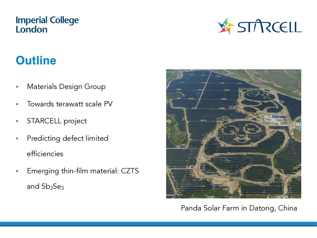
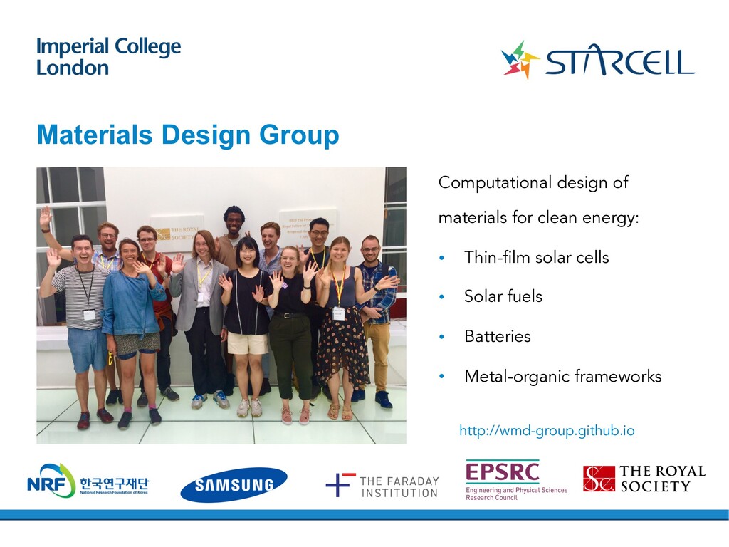
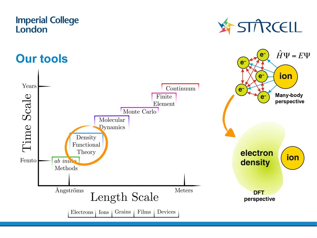
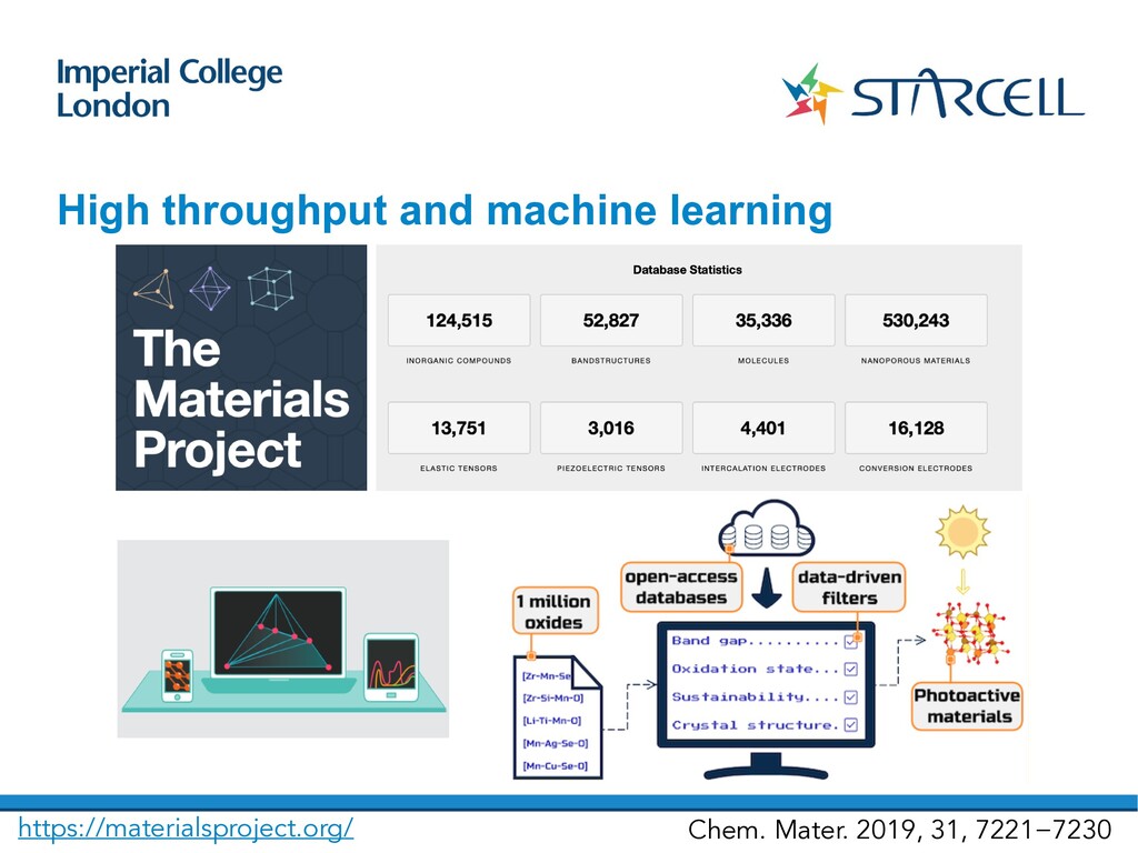
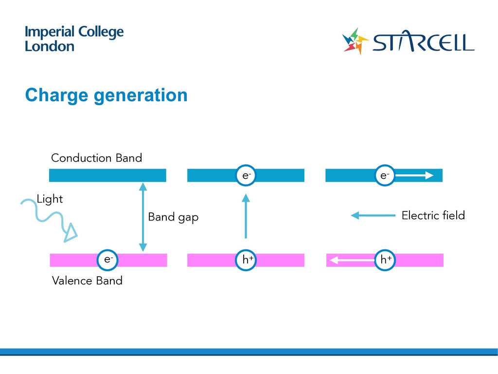
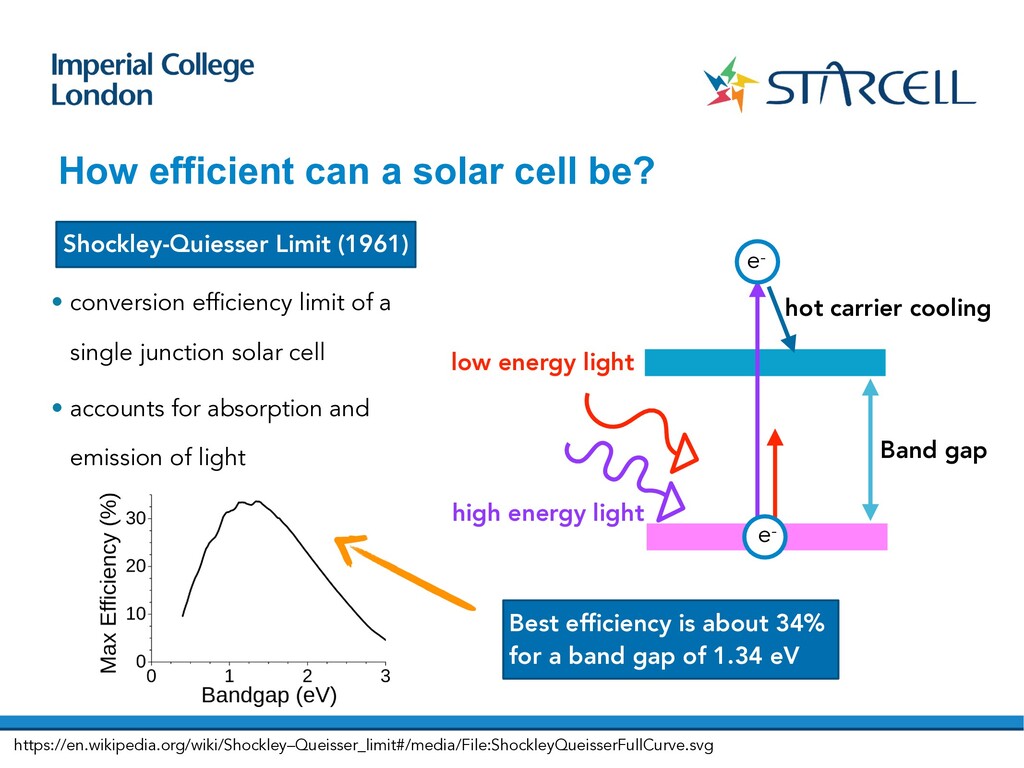
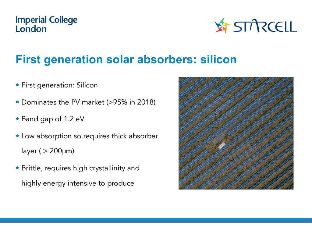
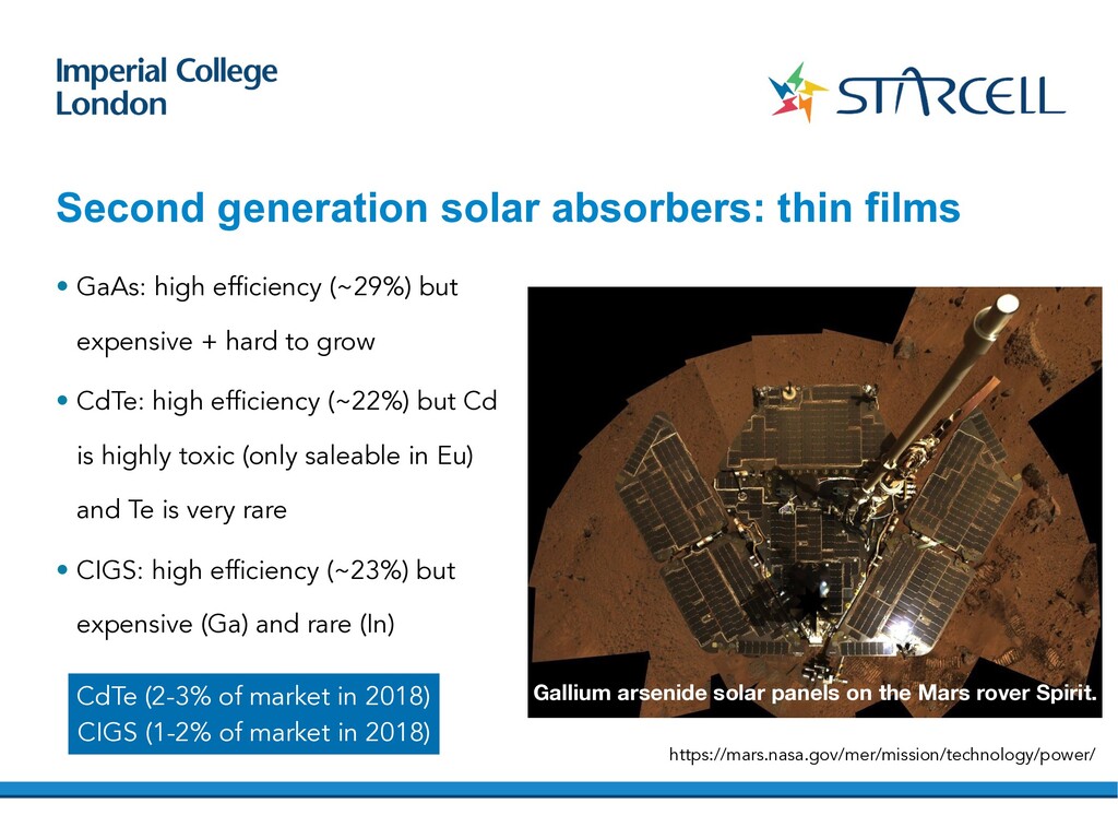
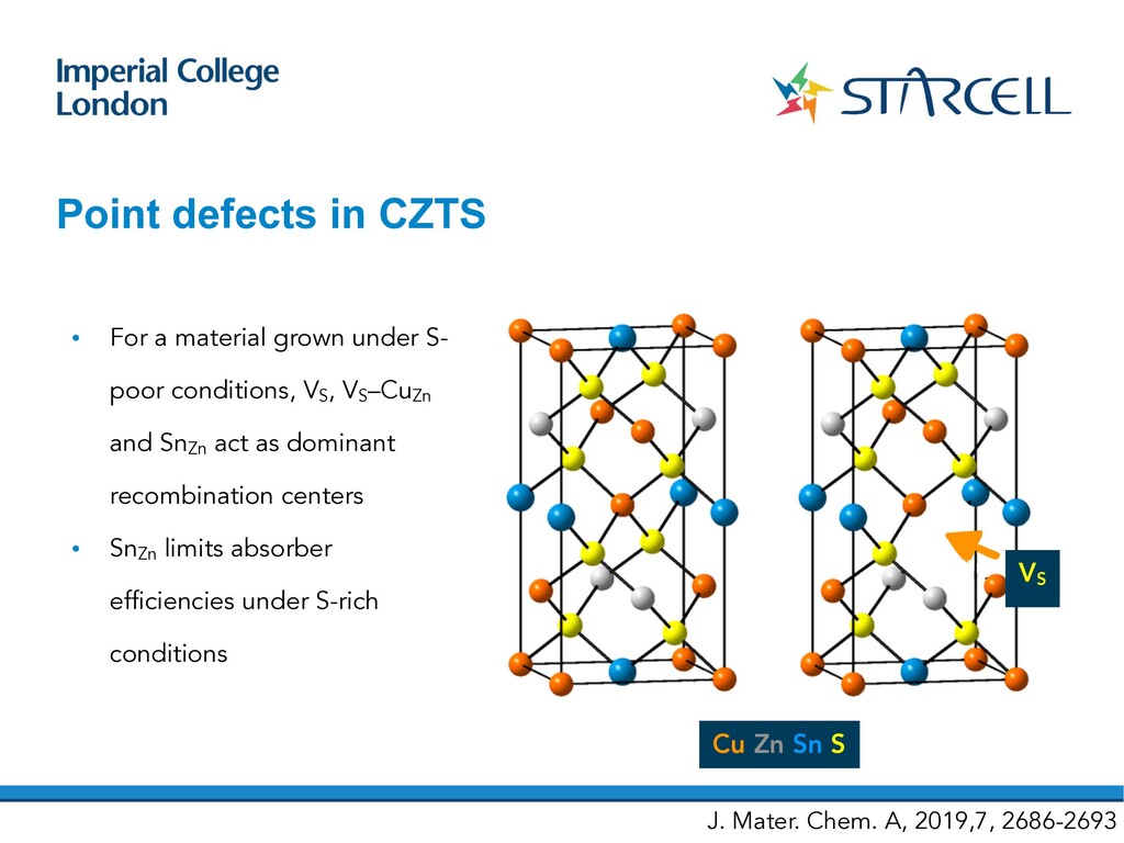
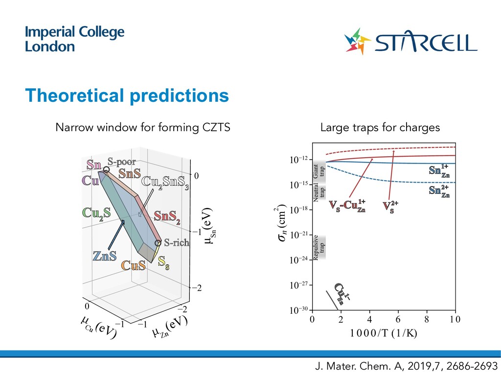
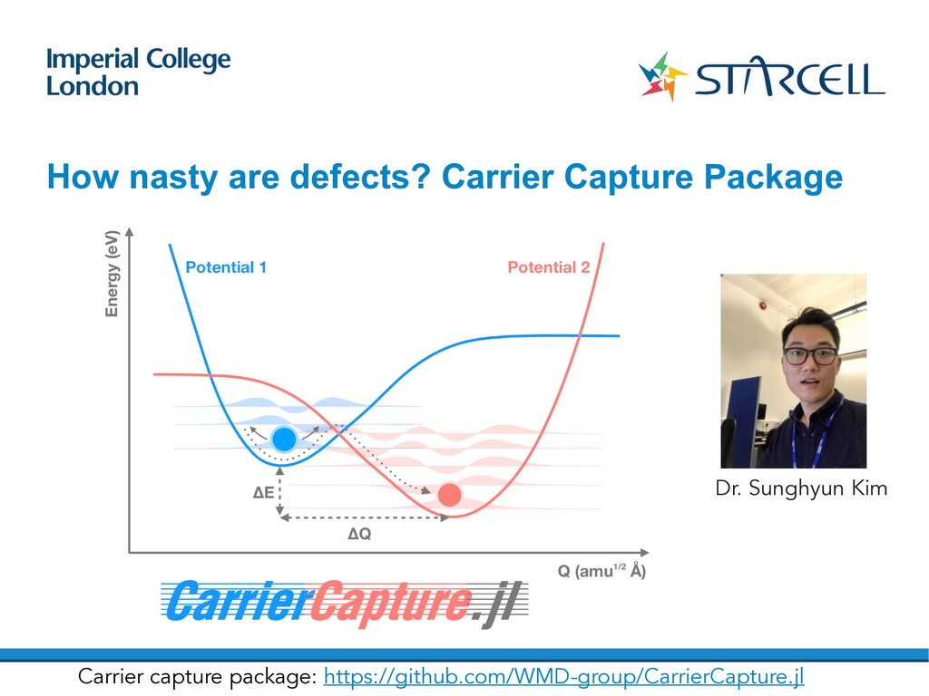
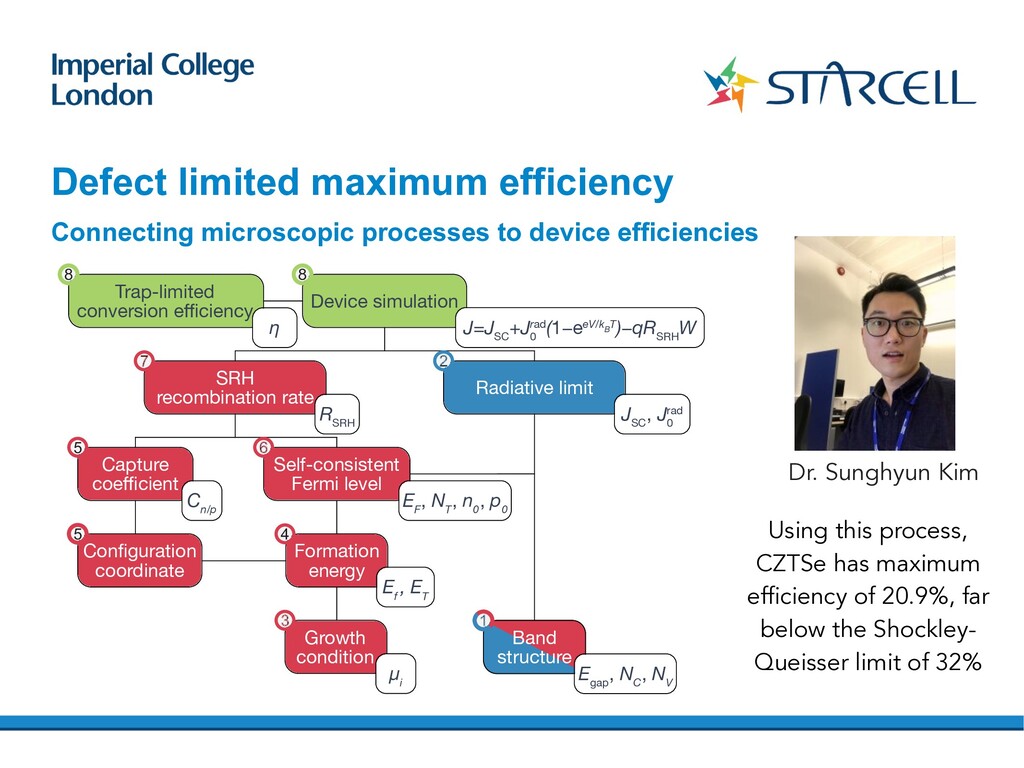
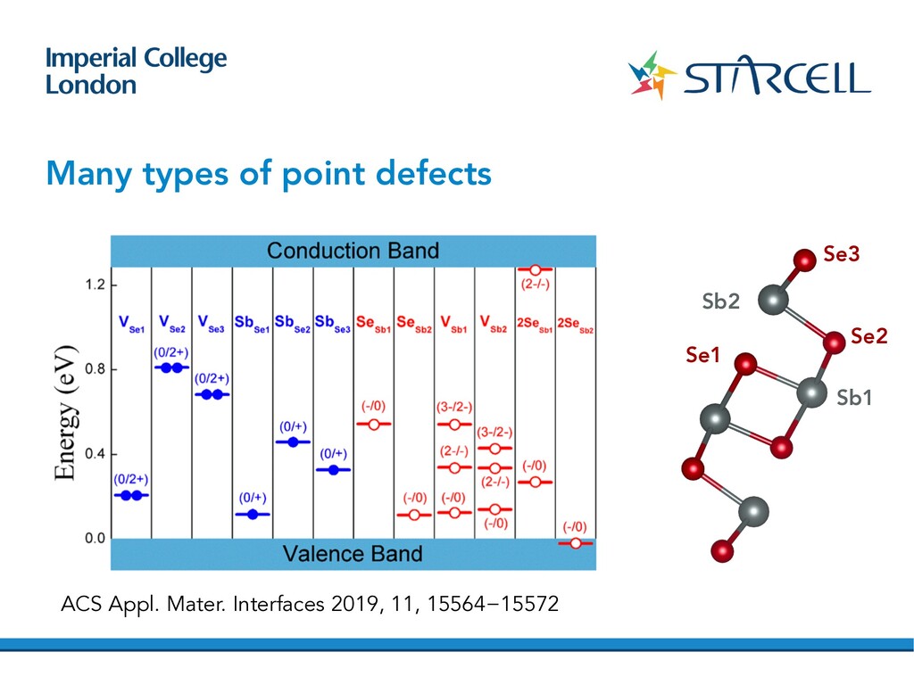
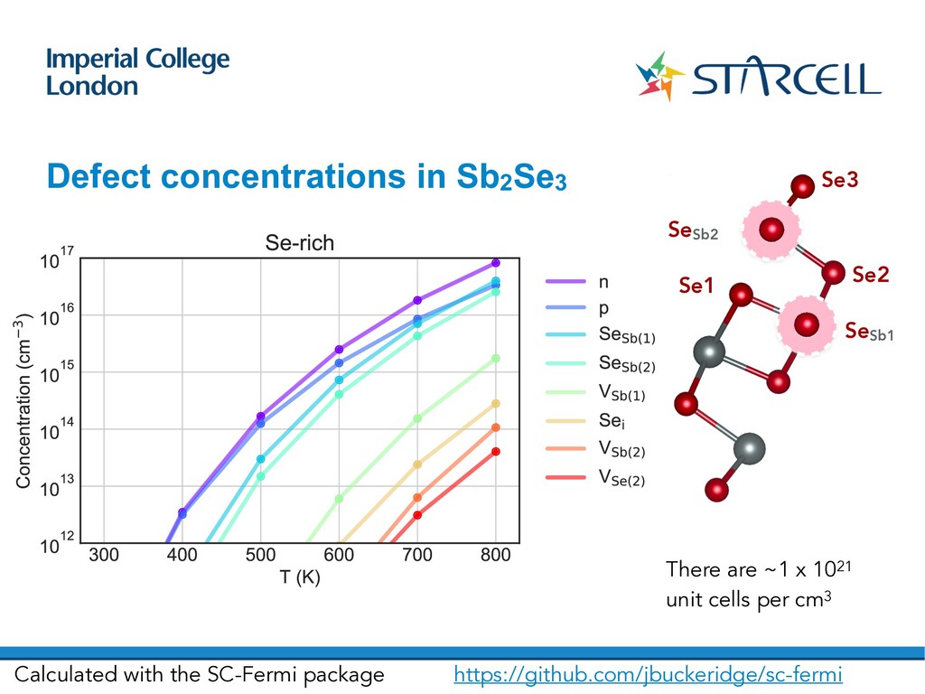
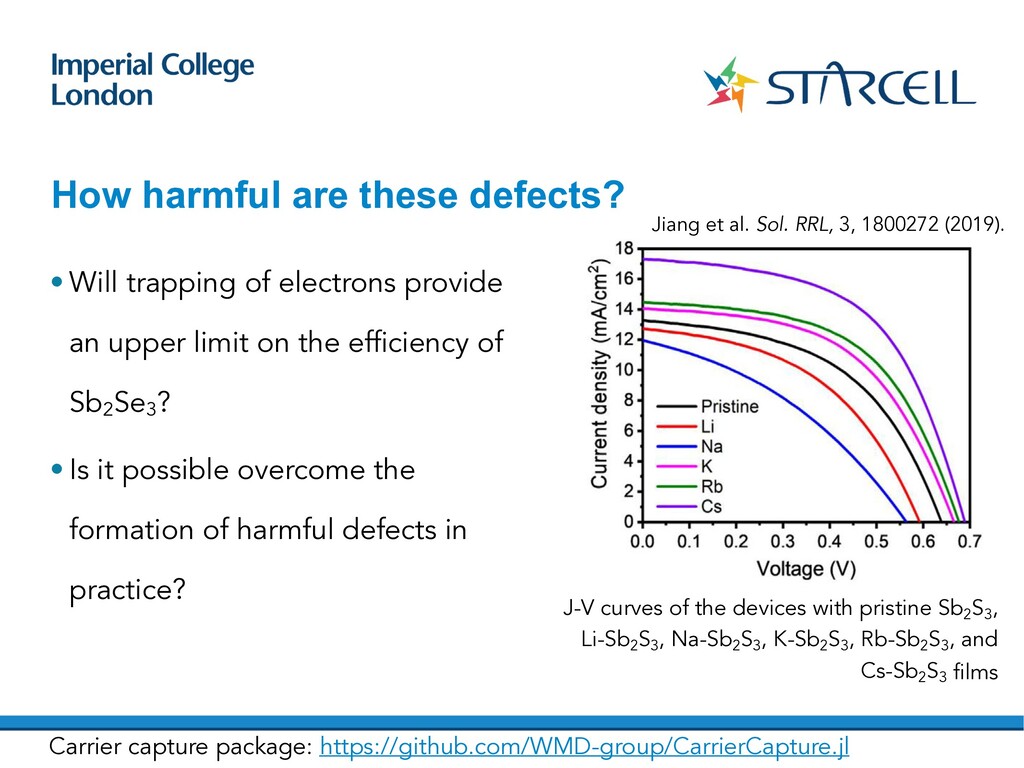
    https://materialsproject.org/ ta-Driven Discovery of Photoactive Quaternary Oxides Using st-Principles Machine Learning iel W. Davies,† Keith T. Butler,‡ and Aron Walsh*,†,§ artment of Materials, Imperial College London, Exhibition Road, London SW7 2AZ, U.K. ML, Scientific Computing Division, Rutherford Appleton Laboratory, Harwell Oxford, Didcot, Oxfordshire OX11 0QX, U.K. bal E3 Institute and Department of Materials Science and Engineering, Yonsei University, Seoul 120-749, Korea Supporting Information BSTRACT: We present a low-cost, virtual high-throughput terials design workflow and use it to identify earth- undant materials for solar energy applications from the aternary oxide chemical space. A statistical model that edicts bandgap from chemical composition is built using pervised machine learning. The trained model forms the t in a hierarchy of screening steps. An ionic substitution orithm is used to assign crystal structures, and an oxidation te probability model is used to discard unlikely chemistries. e demonstrate the utility of this process for screening over 1 llion oxide compositions. We find that, despite the fficulties inherent to identifying stable multicomponent organic materials, several compounds produced by our rkflow are calculated to be thermodynamically stable or metastable and have desirable optoelectronic properties according to t-principles calculations. The predicted oxides are Li2 MnSiO5 , MnAg(SeO3 )2 , and two polymorphs of MnCdGe2 O6 , all four Article pubs.acs.org/cm Cite This: Chem. Mater. 2019, 31, 7221−7230
  8. M A Green Prog. Energy 1 (2019) 013001 Martin A

    Green, Prog. Energy 1 013001 (2019)
  9. • Electricity and transport create 25 billions tonnes of CO2

    annually • 1 TW of PV can displace emissions of 1.5 billion tonnes per year [1] • If we could install 1 TW of PV per year in the next 16 years, we eliminate emissions from these sectors
 Terawatt scale photovoltaics (PV) [1] Martin A Green, Prog. Energy 1 013001 (2019) 1.5 GW Tengger Desert Solar Park, NASA Earth Observatory
  10. Terawatt scale PV predictions PERSPECTIVE NATURE ENERGY Real capacity WBGU

    Greenpeace LIMITS and AMPERE 33rd–66th percentile LIMITS and AMPERE 5th–95th percentile Historic highest/lowest growth rates IEA Real capacity a c b WBGU Greenpeace IEA Installed capacity (GW p ) Installed capacity (GW p ) Growth (%) 103 102 101 100 103 102 104 101 100 1995 2000 2005 Year 2010 2015 2020 2025 2030 Year 2035 2040 2045 2050 2015 1995 100 75 50 25 0 2000 2005 2010 2015 gure 1 | Growth in PV capacity and scenario projections. a, Year-to-year increase of PV capacity as a percentage of the previously installed capacity. , Comparison of historic cumulative installed PV capacity with scenarios from the IEA, Greenpeace and WBGU. c, Scenarios of future cumulative PV RSPECTIVE NATURE ENE Real capacity WBGU Greenpeace LIMITS and AMPERE 33rd–66th percentile LIMITS and AMPERE 5th–95th percentile Historic highest/lowest growth rates IEA Real capacity c WBGU Greenpeace IEA Installed capacity (GW p ) Installed capacity (GW p ) Growth (%) 103 102 101 100 103 102 104 101 100 1995 2000 2005 Year 2010 2015 2020 2025 2030 Year 2035 2040 2045 20 2015 1995 100 75 50 25 0 2000 2005 2010 2015 | Growth in PV capacity and scenario projections. a, Year-to-year increase of PV capacity as a percentage of the previously installed capac parison of historic cumulative installed PV capacity with scenarios from the IEA, Greenpeace and WBGU. c, Scenarios of future cumulative P Creutzig et al. Nature Energy, 2. 17140 (2017)
  11. Terawatt scale PV + thin film absorbers Martin A Green,

    Prog. Energy 1 013001 (2019) • Improving a efficiencies of silicon solar panels by a few percent can greatly accelerate TW scale PV • Adding a thin-film layer on top of silicon to increase absorption could boost efficiencies by ~40% • By mid-century, thin-films may eventually phase out silicon altogether

  12. How does a solar absorber work? Represents average annual spectrum

    for mid latitude locations (AM1.5) Want a material that absorbs sunlight (between 1 to 2 eV) https://www.visionlearning.com/en/library/Earth-Science/6/Factors-that-Control-Earths-Temperature/234
  13. • Absorption of light depends on the band gap and

    absorption strength of the material • Antireflective coatings, solar concentrators Solar absorbers are semiconducting materials https://upload.wikimedia.org/wikipedia/commons/thumb/0/0b/Band_gap_comparison.svg/2000px-Band_gap_comparison.svg.png We want a band gap from 1 to 2 eV
  14. How efficient can a solar cell be? • conversion efficiency

    limit of a single junction solar cell • accounts for absorption and emission of light Shockley-Quiesser Limit (1961) Best efficiency is about 34% for a band gap of 1.34 eV Band gap high energy light e- e- https://en.wikipedia.org/wiki/Shockley–Queisser_limit#/media/File:ShockleyQueisserFullCurve.svg hot carrier cooling low energy light
  15. First generation solar absorbers: silicon • First generation: Silicon •

    Dominates the PV market (>95% in 2018) • Band gap of 1.2 eV • Low absorption so requires thick absorber layer ( > 200μm) • Brittle, requires high crystallinity and highly energy intensive to produce
  16. Second generation solar absorbers: thin films • GaAs: high efficiency

    (~29%) but expensive + hard to grow • CdTe: high efficiency (~22%) but Cd is highly toxic (only saleable in Eu) and Te is very rare • CIGS: high efficiency (~23%) but expensive (Ga) and rare (In) Gallium arsenide solar panels on the Mars rover Spirit. CdTe (2-3% of market in 2018) CIGS (1-2% of market in 2018) https://mars.nasa.gov/mer/mission/technology/power/
  17. How could we use thin film PV? a https://www.inspiredcamping.com/solar-powered-tent/ b

    https://www.alibaba.com/product-detail/Factory-40-Transparent-Amorphous- Silicon-Solar_60732252010.html c https://rotterdam.materialdistrict.com/thin-film-solar-cells/ d https://www.cnet.com/news/tommy-hilfiger-launches-solar-power-jackets-to- charge-your-phone/ e https://www.kickstarter.com/projects/blackhawk-tech/thin-film-solar-charger a) b) d) e) c)
  18. lti Junction Solar Cell How could we use thin films?

    https://www.oxfordpv.com/perovskite-silicon-tandem Tandem solar cells to improve absorption
  19. STARCELL STARCELL aims to develop a cost effective material to

    substitute critical raw materials in PV technologies, based on earth abundant elements with very low toxicity.
  20. Serious threat in the next 100 years Rising threat from

    increased use Limited availability, future risk to supply Synthetic From conflict minerals Elements used in a smart phone Plentiful Supply The 90 natural elements that make up everything How much is there? Is that enough? Read more and play the video game http://bit.ly/euchems-pt This work is licensed under the Creative Commons Attribution-NoDerivs CC-BY-ND H O C Na Mg AI B N F Ca P S CI Si K As Fe Sb Br Pb Rb Be Sr Ba Cs Ra Y Pd Ni Cu Zn Ag Sn Bi Au I Pt W Po At Te Se Hg He Ne Ar Kr Xe Rn GaGe Cd In TI Co Rh Ru Mo Ir Os Re Mn V Ti Zr Nb Hf Fr Th Ac U Pa Sc Ta La Eu Tb Dy Ho Li Cr Gd Er Tm Yb Lu Pr Nd Pm Sm Tc Ce
  21. CZTS solar absorbers • Kesterites are made of low toxicity

    metals (Cu, Sn, and Zn) abundant in the earth's crust. • Kesterite technology is also fully compatible with current CIGS production lines • Current record is 12.6% [2] 11% efficient CZTS, UNSW Cu Zn Sn S [2] Wang et al. Adv. Energy Mater. 4, 1301465 (2014) https://en.wikipedia.org/wiki/CZTS#/media/File:Kristallstruktur_Kesterit.png
  22. Low efficiency due to open circuit voltage (Voc) losses Cu

    Zn Sn S Wang et al. Adv. Energy Mater. 4, 1301465 (2014) ideally, this would be about 820mV Charges are recombining in the absorber material before being extracted
  23. Recombination mechanisms CBM VBM Generation Radiative recombination Auger recombination Hole

    trap Electron trap Recombination centre Non-radiative recombination My aim is to understand non-radiative capture by defects
  24. Point defects in CZTS Cu Zn Sn S Cu Zn

    Sn S VS • For a material grown under S- poor conditions, VS , VS –CuZn and SnZn act as dominant recombination centers • SnZn limits absorber efficiencies under S-rich conditions J. Mater. Chem. A, 2019,7, 2686-2693
  25. Theoretical predictions 0 −1 −1 −2 0 −1 −2 Sn

    ZnS Cu 2 SnS 3 SnS 2 Cu 2 S Cu S 8 SnS CuS μ Zn (eV) μ Cu (eV) μ Sn (eV) S-poor S-rich Sn Cu Zn (b) 2 1 0 1 Energy (eV) 200 ϵ(2 ϵ(1 Neutral trap Repulsive trap Giant trap V S -Cu Zn 1+ V S 2+ Sn Zn 1+ Sn Zn 2+ Cu Sn 1− 1000/T (1/K) σn (cm2) 0 2 4 6 8 10 10−30 10−27 10−24 10−21 10−18 10−15 10−12 (a ) (b) FIG. 6. (a) Electron capture cross-sections of V , V -Cu J. Mater. Chem. A, 2019,7, 2686-2693 Narrow window for forming CZTS Large traps for charges
  26. How nasty are defects? Carrier Capture Package Carrier capture package:

    https://github.com/WMD-group/CarrierCapture.jl Dr. Sunghyun Kim
  27. Defect limited maximum efficiency B n n 0 +Δn N

    J SC J 0 rad(eqV/k B T−1) qR SRH W η max Band structure E gap , N C , N V Growth condition μ i Formation energy E f , E T Configuration coordinate Capture coefficient C n/p Self-consistent Fermi level E F , N T , n 0 , p 0 SRH recombination rate Device simulation Trap-limited conversion efficiency R SRH η Radiative limit J SC , J 0 rad J=J SC +J 0 rad(1−eeV/k B T)−qR SRH W 1 1 2 2 3 4 5 6 6 7 7 8 8 8 5 4 Dr. Sunghyun Kim Using this process, CZTSe has maximum efficiency of 20.9%, far below the Shockley- Queisser limit of 32% Connecting microscopic processes to device efficiencies
  28. d Current density (mA cm–2) 35 30 25 20 15

    10 5 0 JSC (mA/cm2): Area (cm2): VOC (V): FF (%): Eff. (%): 9.2 70.3 32.58 0.40 0.2603 0.4 0.3 0.2 Voltage (V) 0.1 0.0 Fig. 6 Solar cell structure and mechanis glass and finished Sb2 Se3 /CdS core/she solar cells. d, e J-V curve (d) and EQE s Li et al. Nat. Commun. 10, 125 (2019). The problem: low open circuit voltage Grain boundary Experimental Voc ~ 0.4 V [2], about half theoretical limit • Grain boundaries? Intrinsically benign • Point defects? Deceptively difficult
  29. Many types of point defects Sb1 Se2 Se3 Sb2 Se1

    • At first, only 5 defects were considered • Due to low symmetry, there are actually many inequivalent defects Liu et al. Prog. Photovolt: Res. Appl. 25, 861 (2017).
  30. SeSb1 Se3 Se1 Se2 SeSb2 Defect concentrations in Sb2Se3 Calculated

    with the SC-Fermi package https://github.com/jbuckeridge/sc-fermi There are ~1 x 10²¹ unit cells per cm3
  31. • Will trapping of electrons provide an upper limit on

    the efficiency of Sb2 Se3 ? • Is it possible overcome the formation of harmful defects in practice? How harmful are these defects? advancedsciencenews.com J-V curves of the devices with pristine Sb2 S3 , Li-Sb2 S3 , Na-Sb2 S3 , K-Sb2 S3 , Rb-Sb2 S3 , and Cs-Sb2 S3 films Jiang et al. Sol. RRL, 3, 1800272 (2019). Carrier capture package: https://github.com/WMD-group/CarrierCapture.jl
  32. Summary • We need new materials to move towards cheaper,

    more efficient PV at a terawatt scale • Thin-film materials made of earth abundant constituents are ideal for this • We calculate the limitations of these candidate materials, often finding that crystal defects are the efficiency bottlenecks • Developing techniques to enable high-throughput screening of defects in materials to accelerate our search for sustainable thin-film PV materials
  33. Thank you Prof Aron Walsh: Imperial College London & Yonsei

    University Dr Sunghyun Kim: Imperial College London Dr Ji-Sang Park: Kyungpook National University, Korea Dr Chris Savory: University College London Prof David Scanlon: University College London @PaleBlueSam http://wmd-group.github.io