Integrated Circuit Design Reza Molavi Dept. of ECE University of British Columbia [email protected] Slides Courtesy : Dr. Res Saleh (UBC), Dr. D. Sengupta (AMD) and Dr. Mary Jane Irwin (PSU)
the Connect for slide/assignment uploads. (will let you know in class once setup) We will use CAD tools heavily for this course. Course Material: Custom textbook from “Analysis and Design of Digital Integrated Circuits” by D. Hodges and R. Saleh In-class discussion of practical/recent issues of digital IC design frequently encountered in the industry
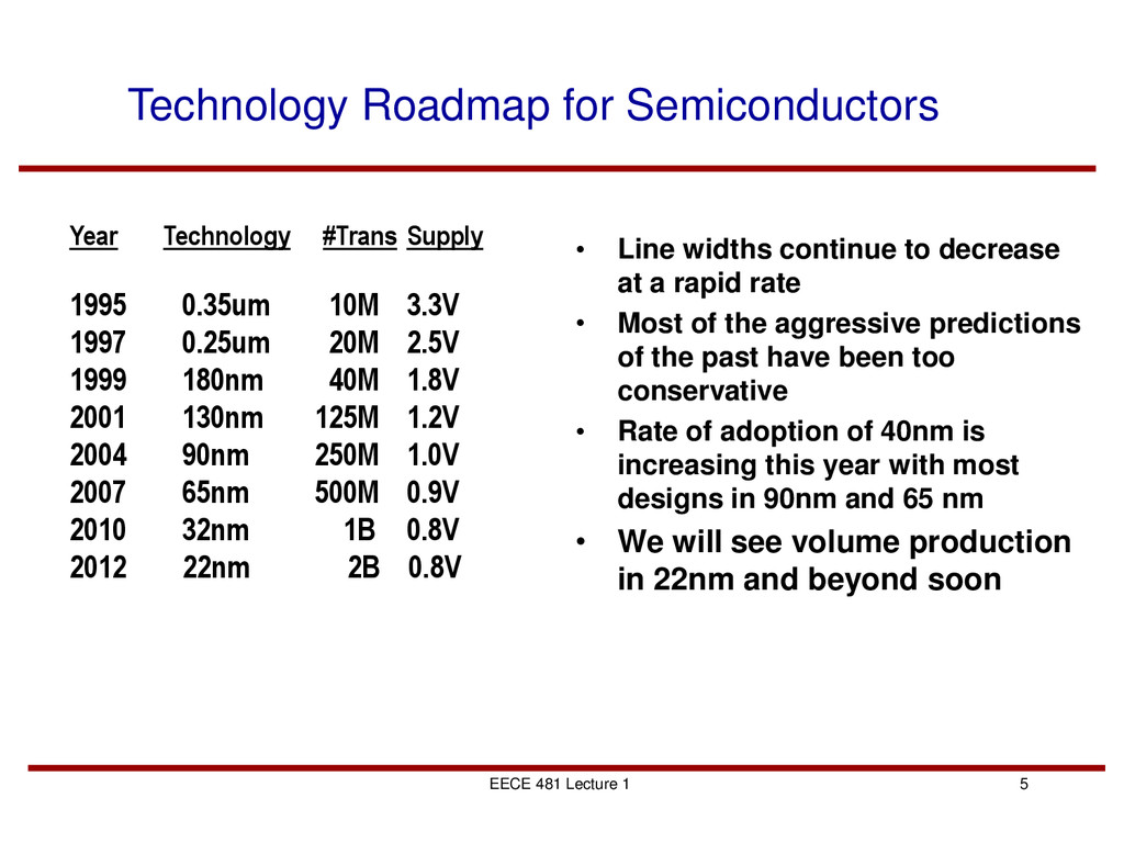
Line widths continue to decrease at a rapid rate • Most of the aggressive predictions of the past have been too conservative • Rate of adoption of 40nm is increasing this year with most designs in 90nm and 65 nm • We will see volume production in 22nm and beyond soon Year Technology #Trans Supply 1995 0.35um 10M 3.3V 1997 0.25um 20M 2.5V 1999 180nm 40M 1.8V 2001 130nm 125M 1.2V 2004 90nm 250M 1.0V 2007 65nm 500M 0.9V 2010 32nm 1B 0.8V 2012 22nm 2B 0.8V
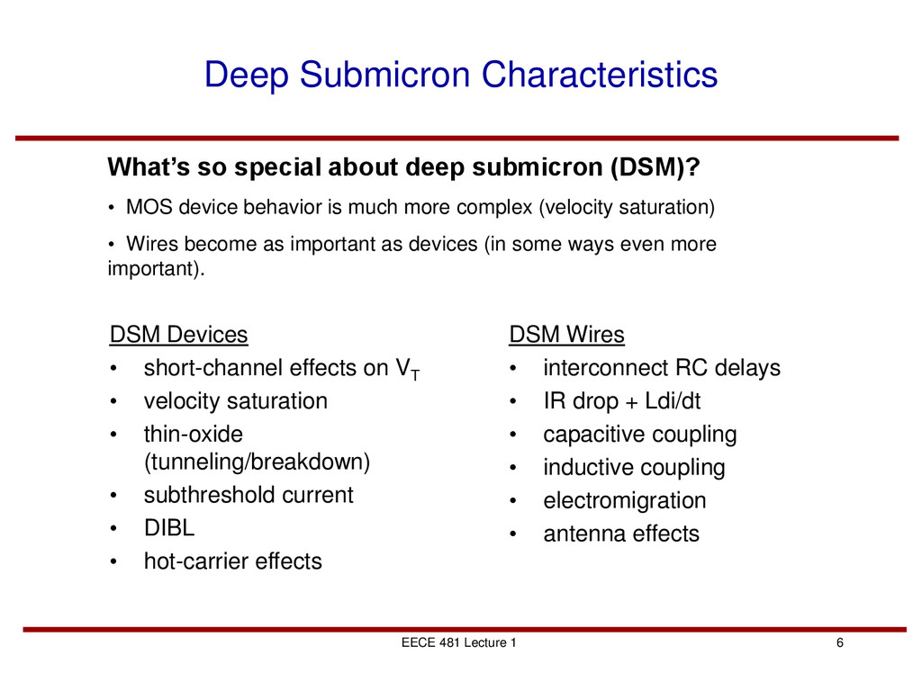
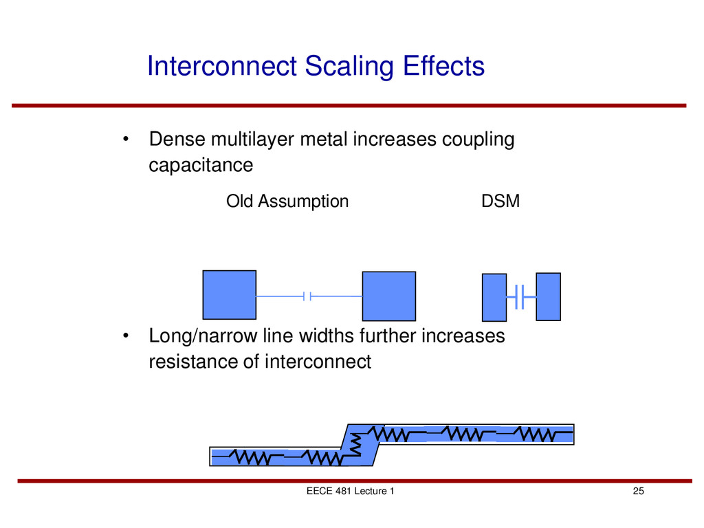
• short-channel effects on VT • velocity saturation • thin-oxide (tunneling/breakdown) • subthreshold current • DIBL • hot-carrier effects DSM Wires • interconnect RC delays • IR drop + Ldi/dt • capacitive coupling • inductive coupling • electromigration • antenna effects What’s so special about deep submicron (DSM)? • MOS device behavior is much more complex (velocity saturation) • Wires become as important as devices (in some ways even more important).
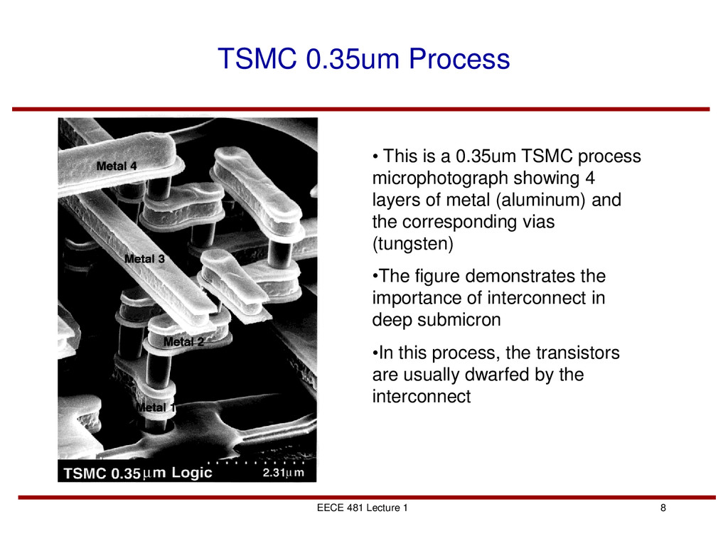
is a 0.35um TSMC process microphotograph showing 4 layers of metal (aluminum) and the corresponding vias (tungsten) •The figure demonstrates the importance of interconnect in deep submicron •In this process, the transistors are usually dwarfed by the interconnect
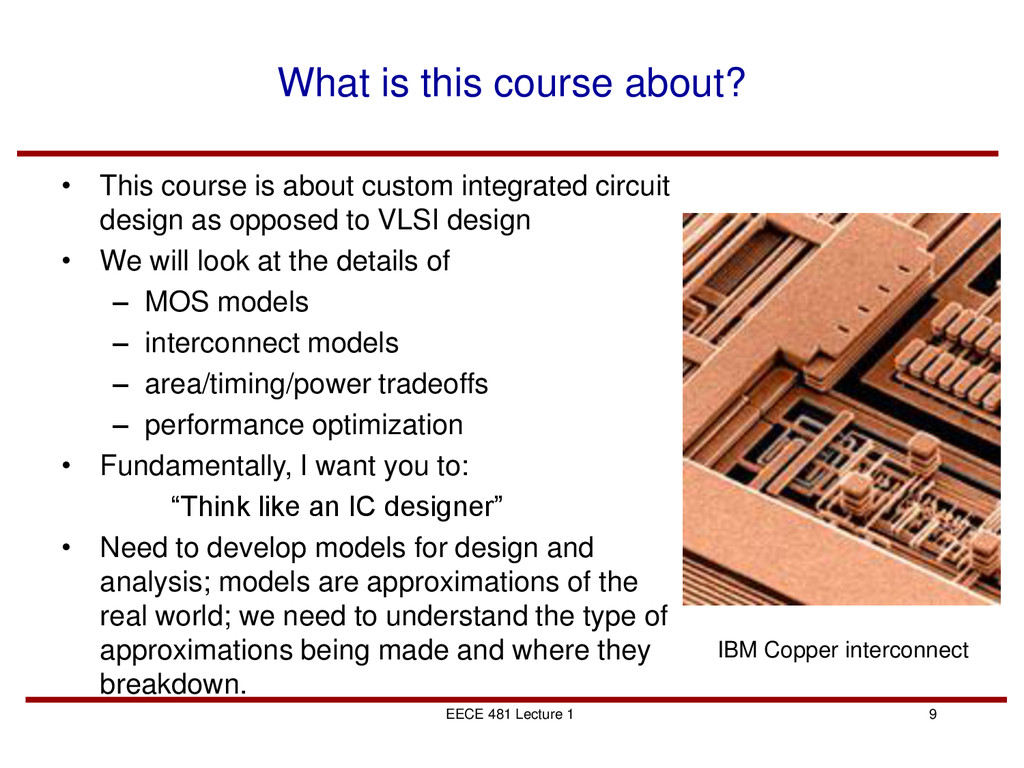
• This course is about custom integrated circuit design as opposed to VLSI design • We will look at the details of – MOS models – interconnect models – area/timing/power tradeoffs – performance optimization • Fundamentally, I want you to: “Think like an IC designer” • Need to develop models for design and analysis; models are approximations of the real world; we need to understand the type of approximations being made and where they breakdown. IBM Copper interconnect
think about: – Innovative configurations of transistors that perform some function better. • Where better might be smaller, faster, lower power, etc. • That is part of the job. The part that takes more time is: – Making sure that this collection of transistors will work OR – Figuring out why this collection of transistors does not work, or only works on a few parts. • To do either, you need to be able to reason about circuits ...
approximation of the real world – Must leave many details out – Must (to be useful) retain the important details – Appropriate level depends on questions you want to answer • CAUTION: – Simulation and analysis do not tell you what the circuit does – It tells you what your MODEL of the circuit does – So remember: • Defect in model directly translates into invalid output results • Some of the hardest work is figuring out the right model for a problem
most widely use circuit simulator for detailed analysis of transistor level designs • It uses very accurate models so we can verify our hand analysis against the “correct” answer • The problem sets will use a version of SPICE called HSPICE. This version has a number of features (like parameter sweeps and optimization) that will make your life easier. • There is a library provided for the class – Consists of models for a 0.18um CMOS technology • One of the review sessions on will explain how to use the key features in HSPICE.
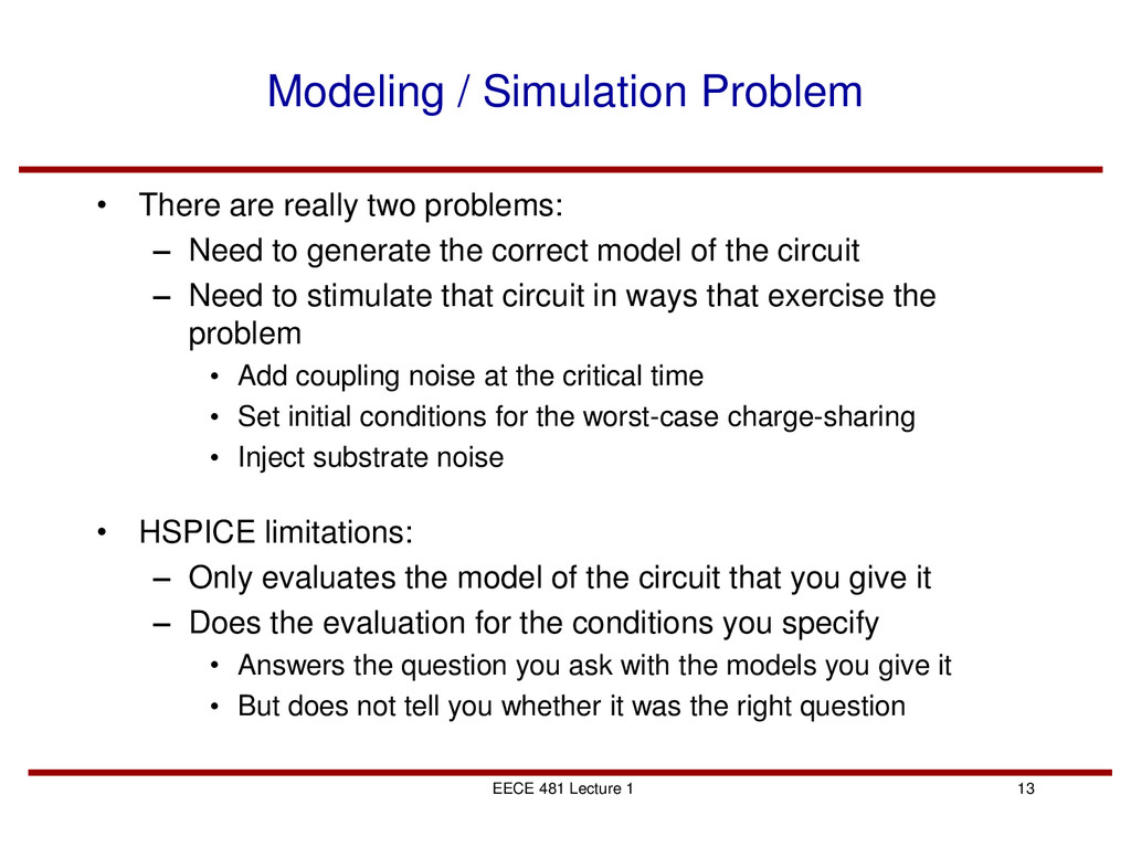
There are really two problems: – Need to generate the correct model of the circuit – Need to stimulate that circuit in ways that exercise the problem • Add coupling noise at the critical time • Set initial conditions for the worst-case charge-sharing • Inject substrate noise • HSPICE limitations: – Only evaluates the model of the circuit that you give it – Does the evaluation for the conditions you specify • Answers the question you ask with the models you give it • But does not tell you whether it was the right question
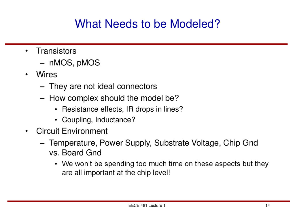
• Transistors – nMOS, pMOS • Wires – They are not ideal connectors – How complex should the model be? • Resistance effects, IR drops in lines? • Coupling, Inductance? • Circuit Environment – Temperature, Power Supply, Substrate Voltage, Chip Gnd vs. Board Gnd • We won’t be spending too much time on these aspects but they are all important at the chip level!
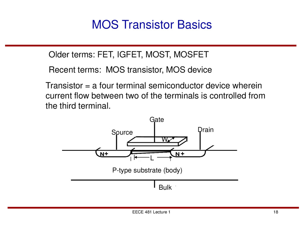
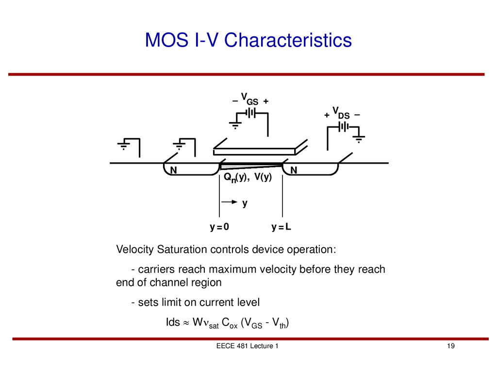
FET, IGFET, MOST, MOSFET Recent terms: MOS transistor, MOS device Transistor = a four terminal semiconductor device wherein current flow between two of the terminals is controlled from the third terminal. N N – V GS + + V DS – y y = 0 y = L Q (y), V(y) n P-type substrate (body) + + Source Gate Drain Bulk L W
– V GS + + V DS – y y = 0 y = L Q (y), V(y) n Velocity Saturation controls device operation: - carriers reach maximum velocity before they reach end of channel region - sets limit on current level Ids Wnsat Cox (VGS - Vth )
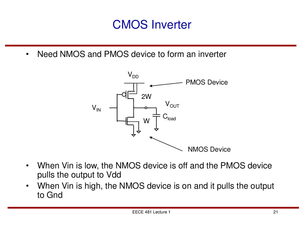
and PMOS device to form an inverter • When Vin is low, the NMOS device is off and the PMOS device pulls the output to Vdd • When Vin is high, the NMOS device is on and it pulls the output to Gnd 2W W Cload PMOS Device NMOS Device VIN VOUT VDD
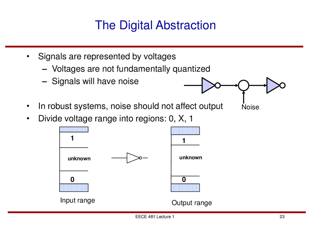
are represented by voltages – Voltages are not fundamentally quantized – Signals will have noise • In robust systems, noise should not affect output • Divide voltage range into regions: 0, X, 1 1 0 unknown 1 0 unknown Output range Input range Noise
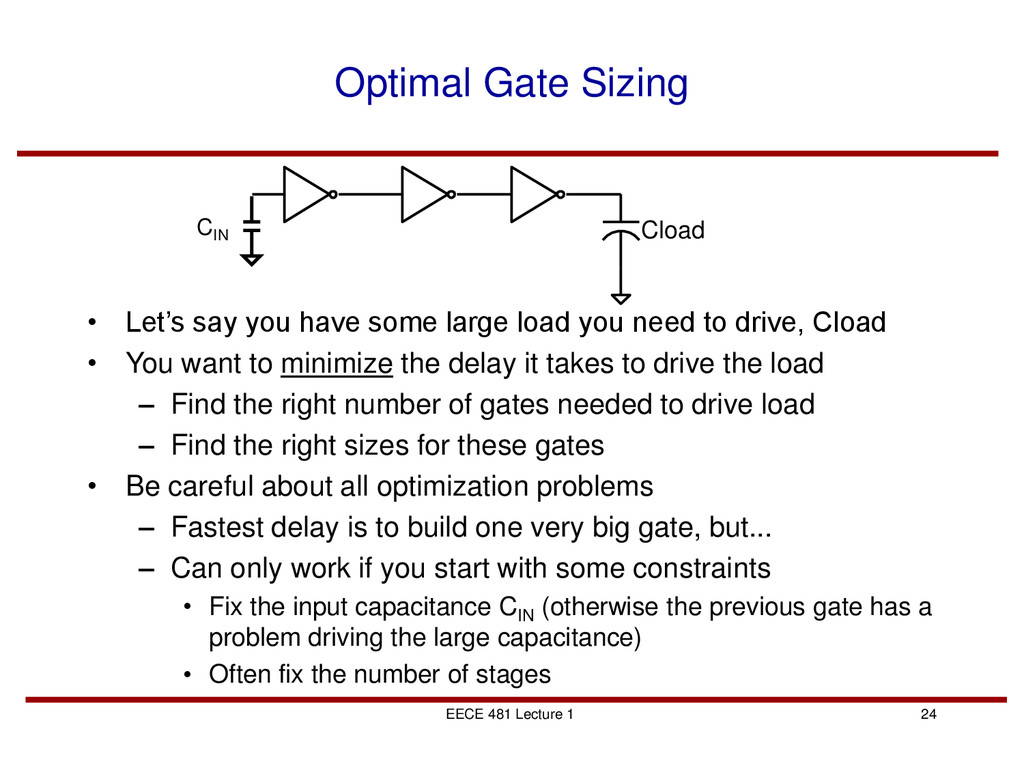
say you have some large load you need to drive, Cload • You want to minimize the delay it takes to drive the load – Find the right number of gates needed to drive load – Find the right sizes for these gates • Be careful about all optimization problems – Fastest delay is to build one very big gate, but... – Can only work if you start with some constraints • Fix the input capacitance CIN (otherwise the previous gate has a problem driving the large capacitance) • Often fix the number of stages Cload CIN
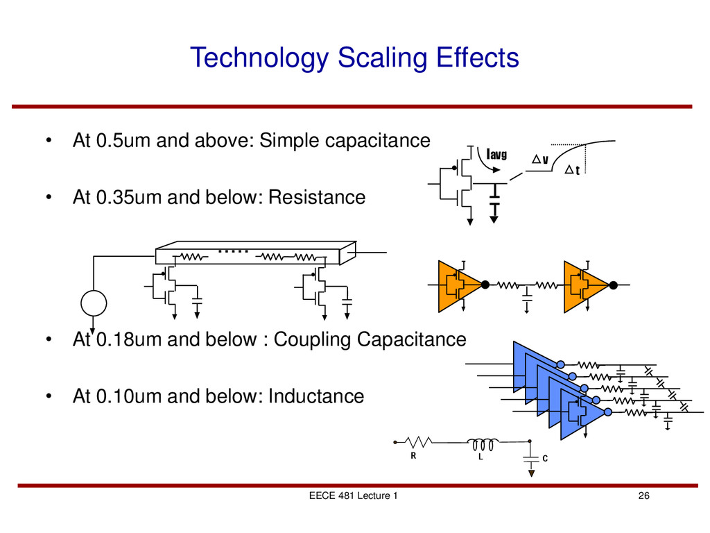
0.5um and above: Simple capacitance • At 0.35um and below: Resistance • At 0.18um and below : Coupling Capacitance • At 0.10um and below: Inductance t v Iavg ..... R L C
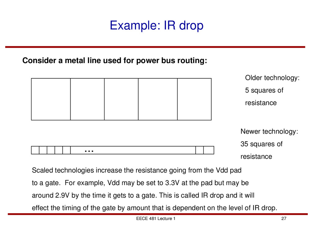
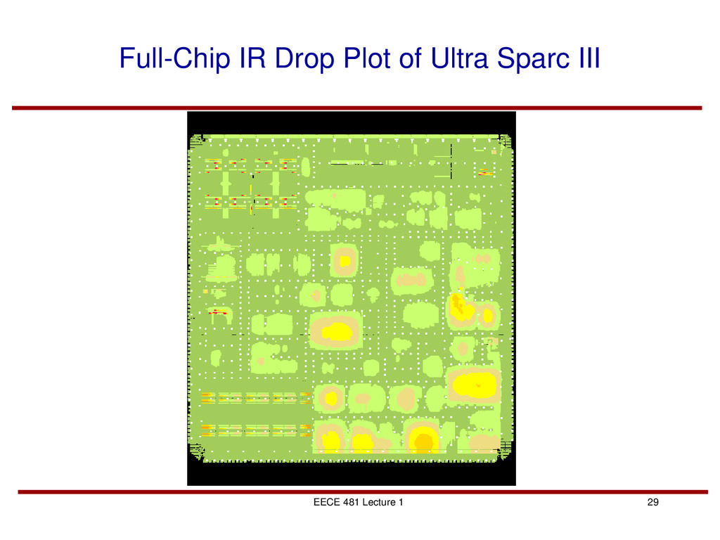
technology: 5 squares of resistance Newer technology: 35 squares of resistance Consider a metal line used for power bus routing: Scaled technologies increase the resistance going from the Vdd pad to a gate. For example, Vdd may be set to 3.3V at the pad but may be around 2.9V by the time it gets to a gate. This is called IR drop and it will effect the timing of the gate by amount that is dependent on the level of IR drop.
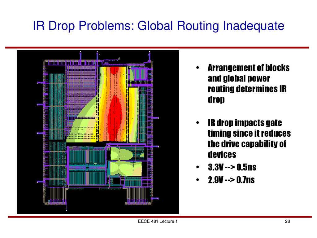
Inadequate • Arrangement of blocks and global power routing determines IR drop • IR drop impacts gate timing since it reduces the drive capability of devices • 3.3V --> 0.5ns • 2.9V --> 0.7ns
introduced new issues in MOS integrated circuit design for both devices and interconnect • In order to understand these issues, and design in the presence of the new problems, we need to understand the device and interconnect models in detail • This course will give you the background you need to design in 0.18um and 0.13um technologies ( and 90nm too!!) • Also, I think it is a lot of fun, and I hope you will find it interesting