Share
Embed
ECOS: An RTL-to-Chip Design Solution with Open-Source EDA, IP, and PDKs
Open Sillicon project from China

TAKASU Masakazu
November 16, 2026
Transcript
43 slides
-
EDA, Chip, One Student One Chip, System ECOS Team ECOS:
An RTL-to-Chip Design Solution with Open-Source EDA, IP, and PDKs Biwei Xie [email protected] Associate Professor ICT, Chinese Academy of Sciences November 11, 2026 -
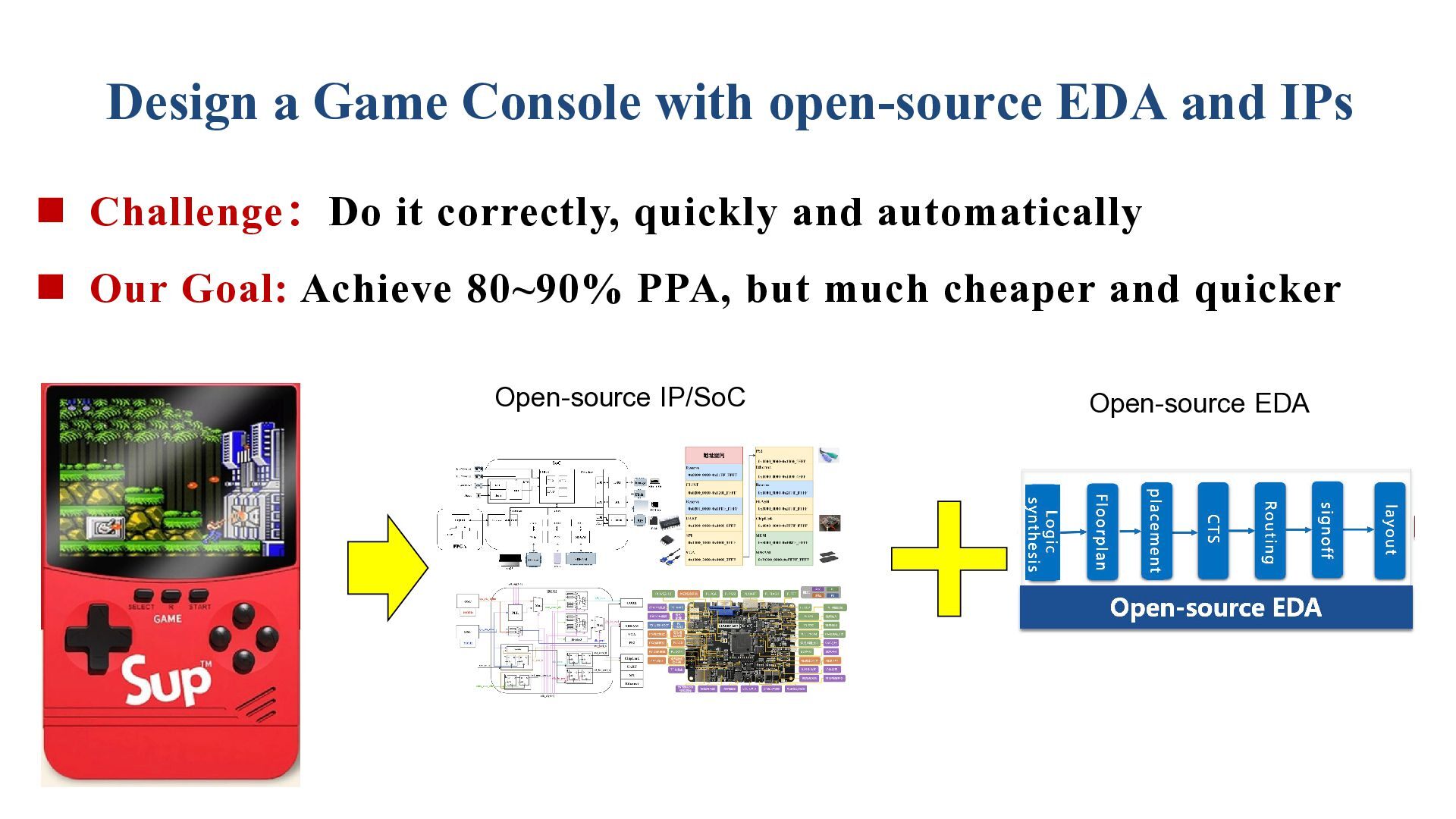
Design a Game Console with open-source EDA and IPs
Challenge:Do it correctly, quickly and automatically Our Goal: Achieve 80~90% PPA, but much cheaper and quicker Open-source IP/SoC Open-source EDA -
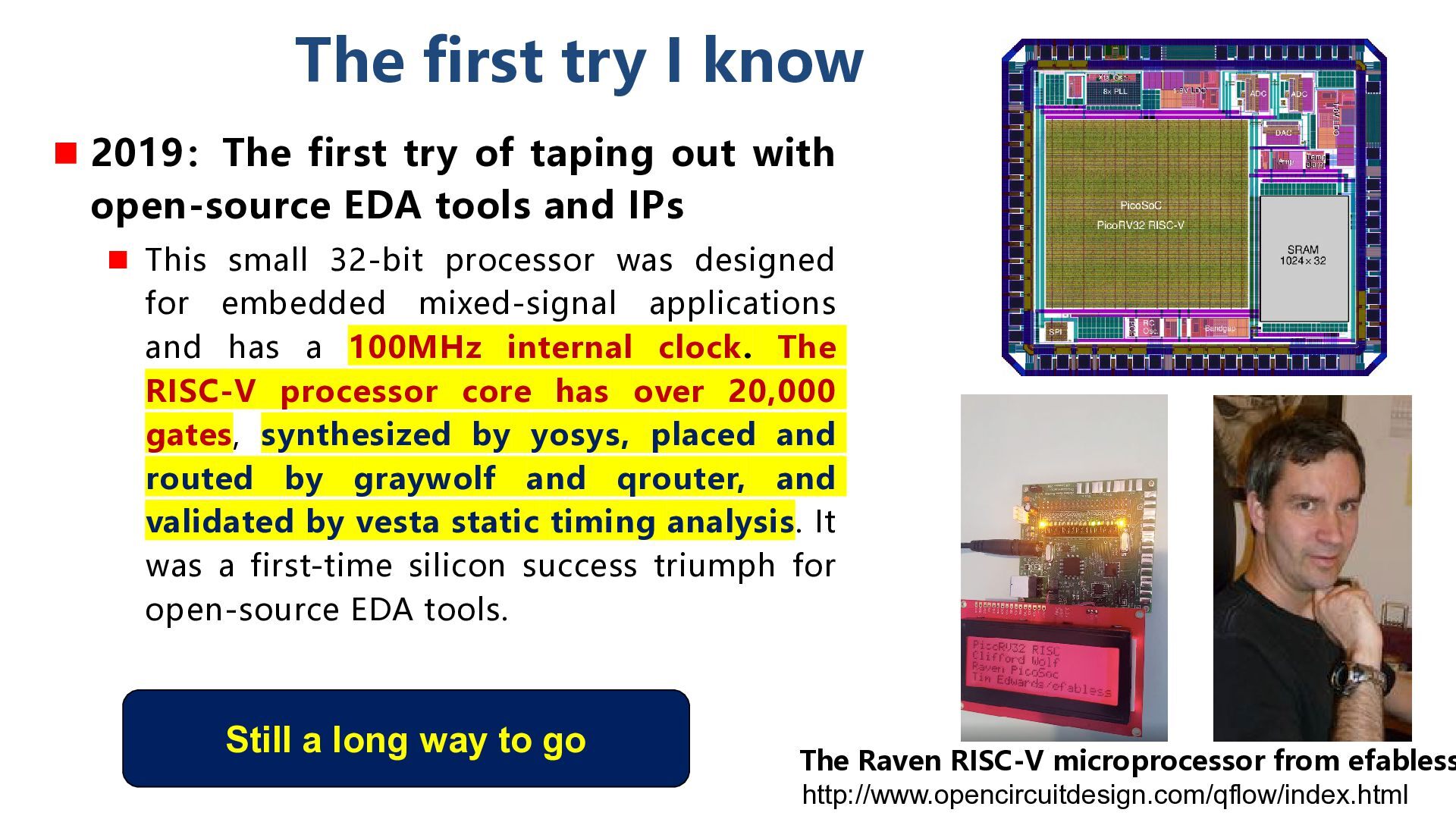
The first try I know 2019:The first try of
taping out with open-source EDA tools and IPs This small 32-bit processor was designed for embedded mixed-signal applications and has a 100MHz internal clock. The RISC-V processor core has over 20,000 gates, synthesized by yosys, placed and routed by graywolf and qrouter, and validated by vesta static timing analysis. It was a first-time silicon success triumph for open-source EDA tools. Still a long way to go The Raven RISC-V microprocessor from efabless http://www.opencircuitdesign.com/qflow/index.html -
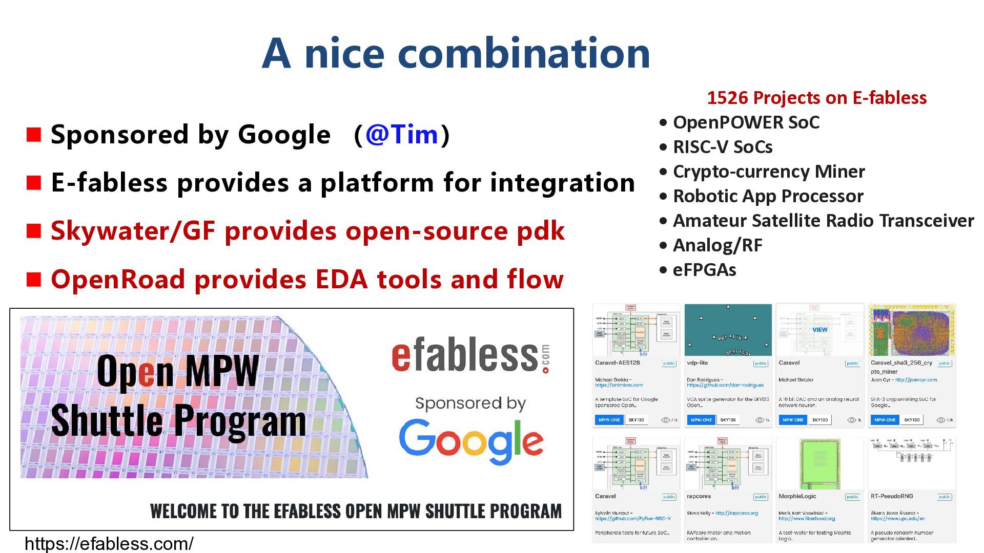
A nice combination Sponsored by Google (@Tim) E-fabless
provides a platform for integration Skywater/GF provides open-source pdk OpenRoad provides EDA tools and flow https://efabless.com/ 1526 Projects on E-fabless • OpenPOWER SoC • RISC-V SoCs • Crypto-currency Miner • Robotic App Processor • Amateur Satellite Radio Transceiver • Analog/RF • eFPGAs -
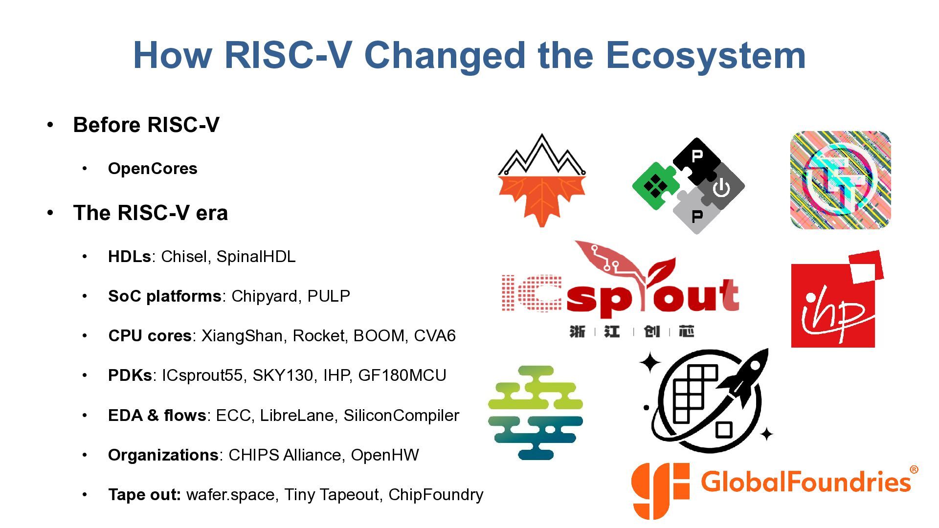
How RISC-V Changed the Ecosystem • Before RISC-V • OpenCores
• The RISC-V era • HDLs: Chisel, SpinalHDL • SoC platforms: Chipyard, PULP • CPU cores: XiangShan, Rocket, BOOM, CVA6 • PDKs: ICsprout55, SKY130, IHP, GF180MCU • EDA & flows: ECC, LibreLane, SiliconCompiler • Organizations: CHIPS Alliance, OpenHW • Tape out: wafer.space, Tiny Tapeout, ChipFoundry -
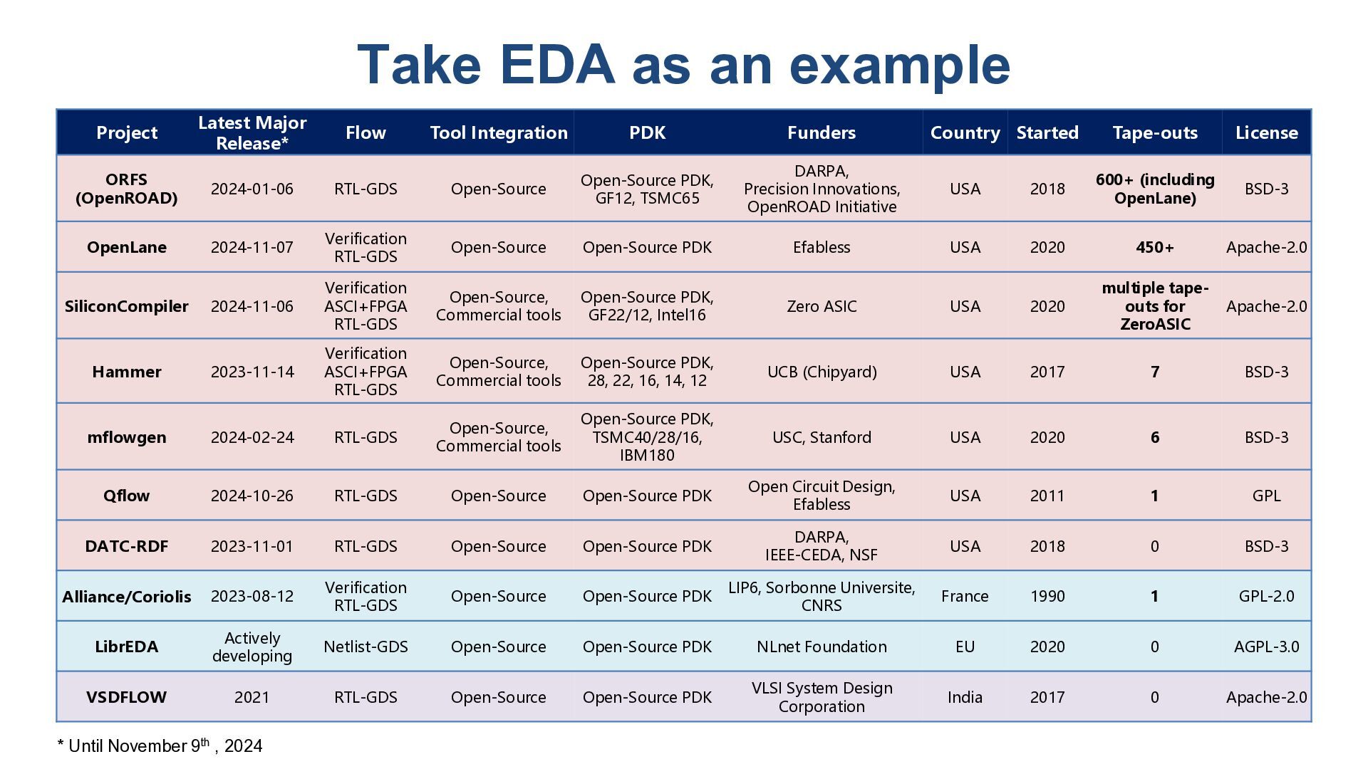
Take EDA as an example Project Latest Major Release* Flow
Tool Integration PDK Funders Country Started DARPA, Precision Innovations, OpenROAD Initiative USA Tape-outs License 2018 600+ (including OpenLane) BSD-3 ORFS (OpenROAD) 2024-01-06 RTL-GDS Open-Source Open-Source PDK, GF12, TSMC65 OpenLane 2024-11-07 Verification RTL-GDS Open-Source Open-Source PDK Efabless USA 2020 450+ Apache-2.0 SiliconCompiler 2024-11-06 Verification ASCI+FPGA RTL-GDS Open-Source, Commercial tools Open-Source PDK, GF22/12, Intel16 Zero ASIC USA 2020 multiple tapeouts for ZeroASIC Apache-2.0 Hammer 2023-11-14 Verification ASCI+FPGA RTL-GDS Open-Source, Commercial tools Open-Source PDK, 28, 22, 16, 14, 12 UCB (Chipyard) USA 2017 7 BSD-3 mflowgen 2024-02-24 RTL-GDS Open-Source, Commercial tools Open-Source PDK, TSMC40/28/16, IBM180 USC, Stanford USA 2020 6 BSD-3 Qflow 2024-10-26 RTL-GDS Open-Source Open-Source PDK Open Circuit Design, Efabless USA 2011 1 GPL DATC-RDF 2023-11-01 RTL-GDS Open-Source Open-Source PDK DARPA, IEEE-CEDA, NSF USA 2018 0 BSD-3 Alliance/Coriolis 2023-08-12 Verification RTL-GDS Open-Source Open-Source PDK LIP6, Sorbonne Universite, CNRS France 1990 1 GPL-2.0 LibrEDA Actively developing Netlist-GDS Open-Source Open-Source PDK NLnet Foundation EU 2020 0 AGPL-3.0 VSDFLOW 2021 RTL-GDS Open-Source Open-Source PDK VLSI System Design Corporation India 2017 0 Apache-2.0 * Until November 9th , 2024 -
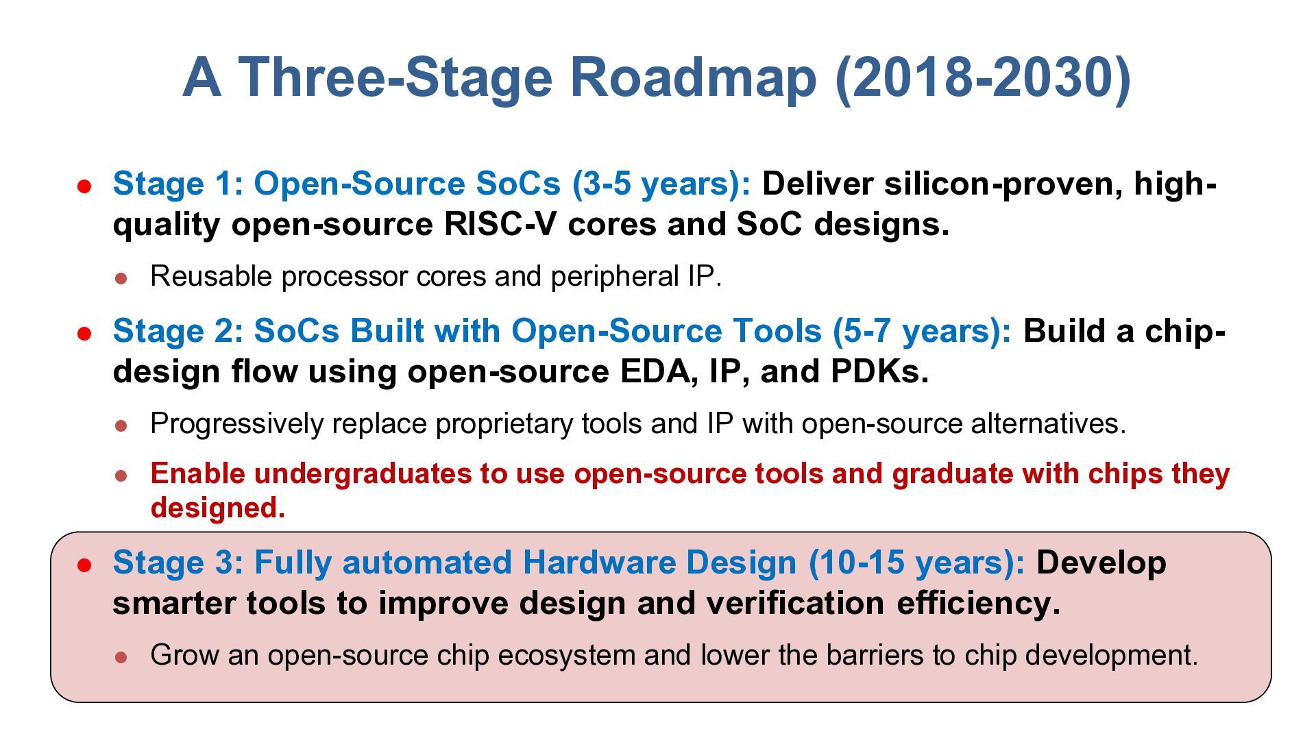
A Three-Stage Roadmap (2018-2030) Stage 1: Open-Source SoCs (3-5
years): Deliver silicon-proven, highquality open-source RISC-V cores and SoC designs. Stage 2: SoCs Built with Open-Source Tools (5-7 years): Build a chipdesign flow using open-source EDA, IP, and PDKs. Reusable processor cores and peripheral IP. Progressively replace proprietary tools and IP with open-source alternatives. Enable undergraduates to use open-source tools and graduate with chips they designed. Stage 3: Fully automated Hardware Design (10-15 years): Develop smarter tools to improve design and verification efficiency. Grow an open-source chip ecosystem and lower the barriers to chip development. -
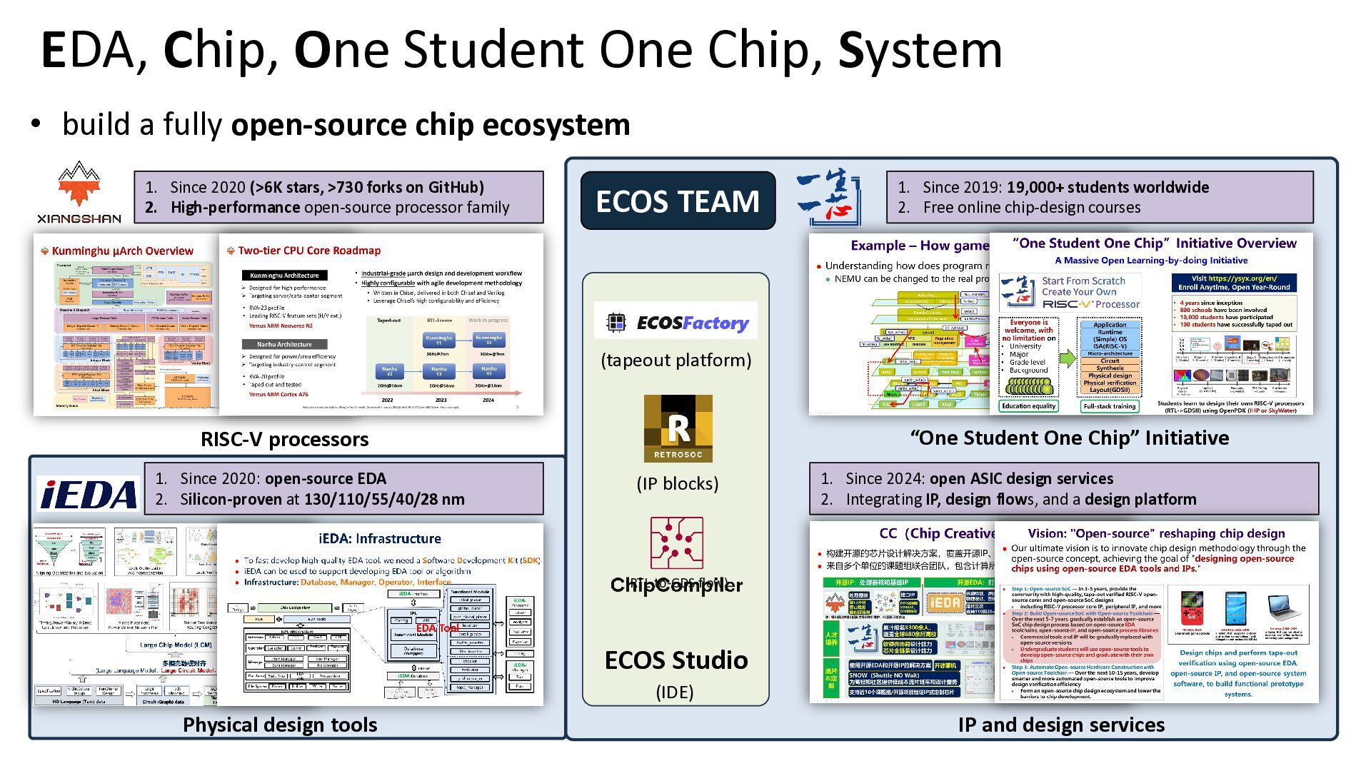
EDA, Chip, One Student One Chip, System • build a
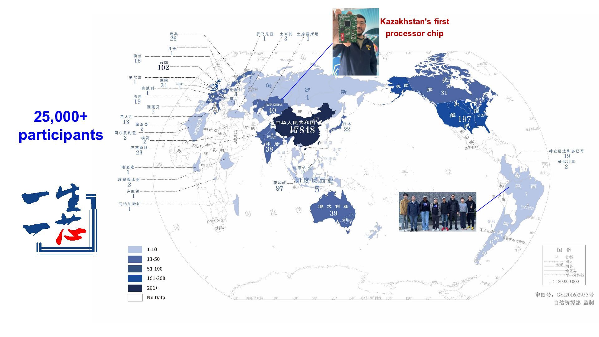
fully open-source chip ecosystem 1. Since 2020 (>6K stars, >730 forks on GitHub) 2. High-performance open-source processor family ECOS TEAM 1. Since 2019: 19,000+ students worldwide 2. Free online chip-design courses (tapeout platform) “One Student One Chip” Initiative RISC-V processors 1. Since 2020: open-source EDA 2. Silicon-proven at 130/110/55/40/28 nm (IP blocks) 1. Since 2024: open ASIC design services 2. Integrating IP, design flows, and a design platform (RTL-to-GDS flow) ECOS Studio (IDE) Physical design tools IP and design services -
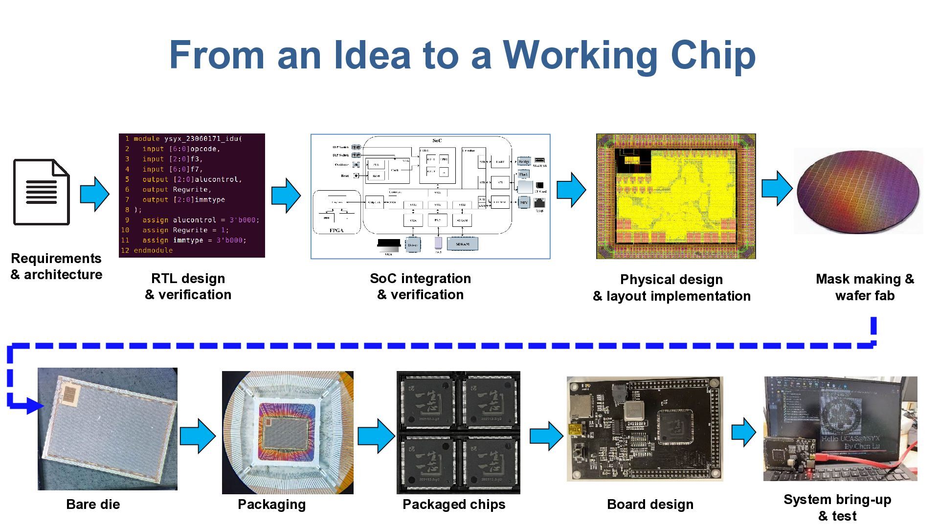
From an Idea to a Working Chip Requirements & architecture
Bare die RTL design & verification SoC integration & verification Packaging Packaged chips Physical design & layout implementation Board design Mask making & wafer fab System bring-up & test -
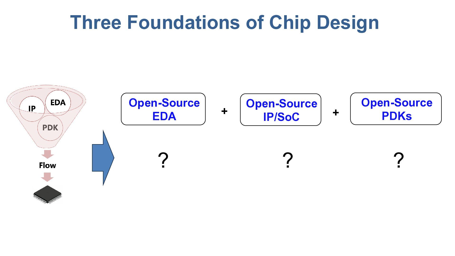
Three Foundations of Chip Design Open-Source EDA ? + Open-Source
IP/SoC ? + Open-Source PDKs ? -
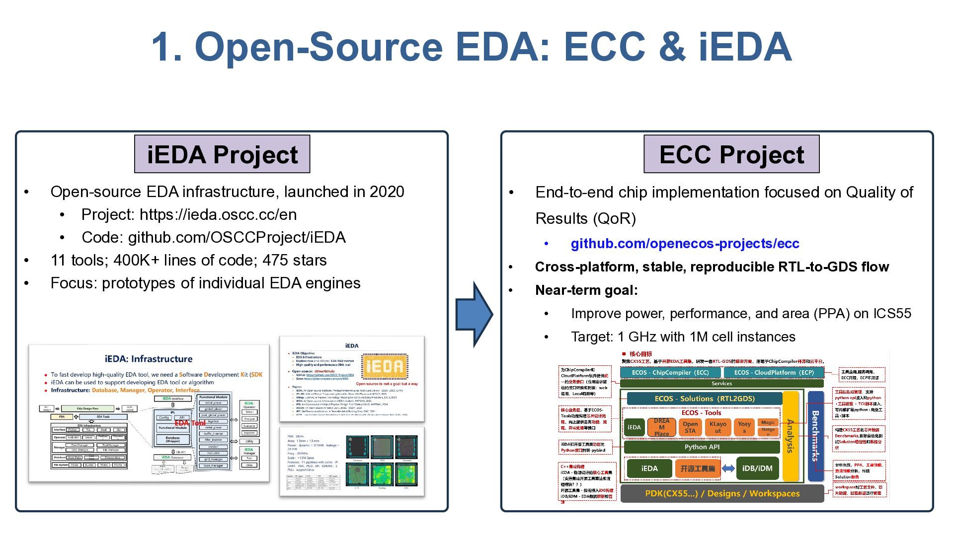
1. Open-Source EDA: ECC & iEDA iEDA Project • •
• Open-source EDA infrastructure, launched in 2020 • Project: https://ieda.oscc.cc/en • Code: github.com/OSCCProject/iEDA 11 tools; 400K+ lines of code; 475 stars Focus: prototypes of individual EDA engines ECC Project • End-to-end chip implementation focused on Quality of Results (QoR) • github.com/openecos-projects/ecc • Cross-platform, stable, reproducible RTL-to-GDS flow • Near-term goal: • Improve power, performance, and area (PPA) on ICS55 • Target: 1 GHz with 1M cell instances -
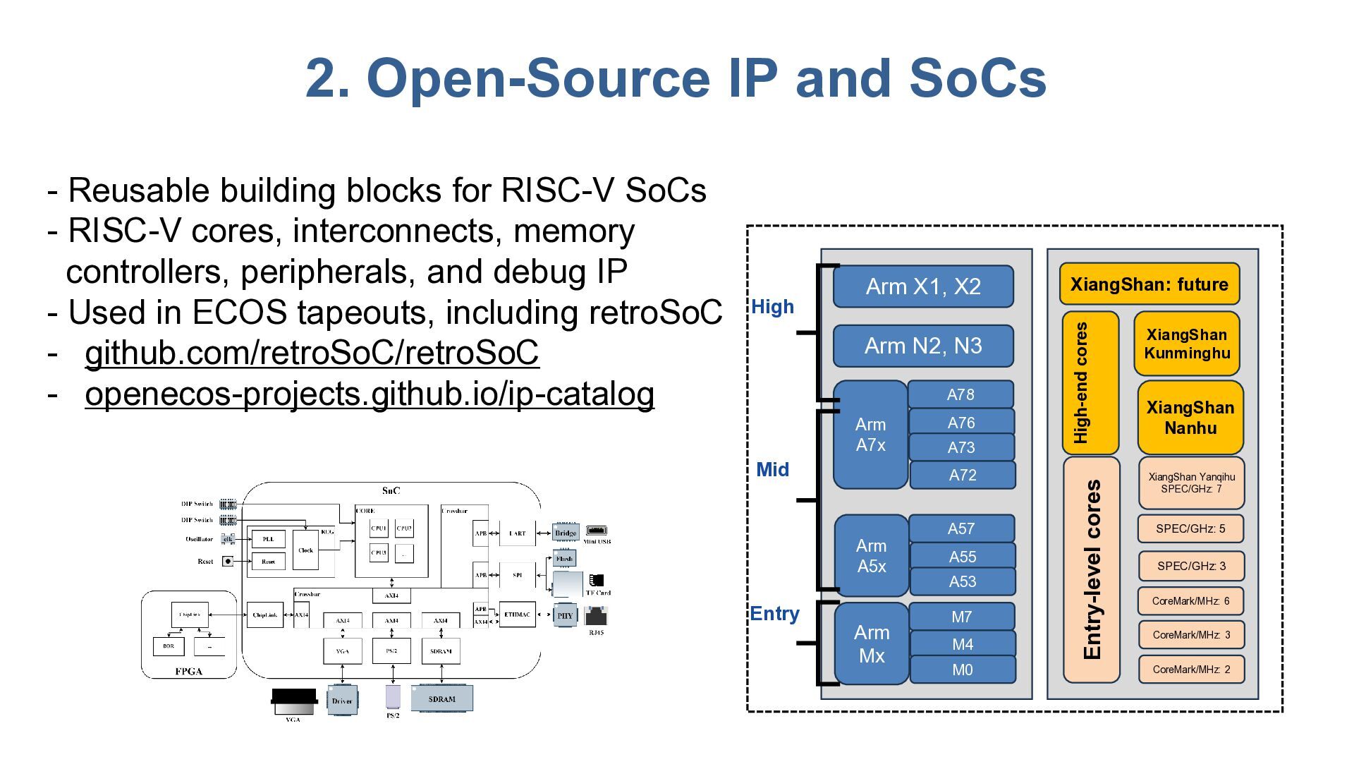
2. Open-Source IP and SoCs Arm N2, N3 A78 Mid
Arm A7x A73 A72 Arm A5x Entry A76 Arm Mx A57 A55 A53 M7 M4 M0 XiangShan: future High-end cores High Arm X1, X2 Entry-level cores - Reusable building blocks for RISC-V SoCs - RISC-V cores, interconnects, memory controllers, peripherals, and debug IP - Used in ECOS tapeouts, including retroSoC - github.com/retroSoC/retroSoC - openecos-projects.github.io/ip-catalog XiangShan Kunminghu XiangShan Nanhu XiangShan Yanqihu SPEC/GHz: 7 SPEC/GHz: 5 SPEC/GHz: 3 CoreMark/MHz: 6 CoreMark/MHz: 3 CoreMark/MHz: 2 -
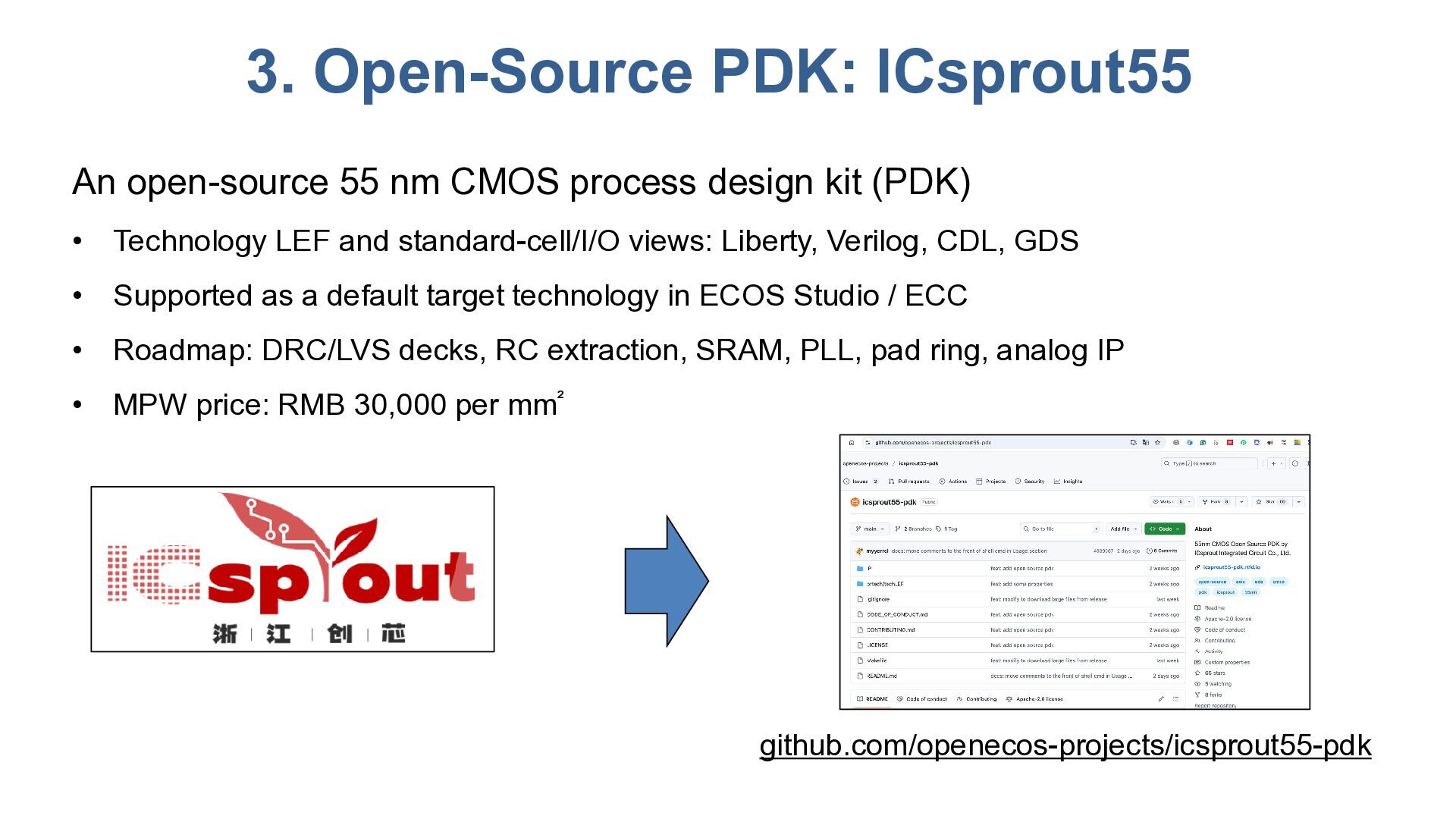
3. Open-Source PDK: ICsprout55 An open-source 55 nm CMOS process
design kit (PDK) • Technology LEF and standard-cell/I/O views: Liberty, Verilog, CDL, GDS • Supported as a default target technology in ECOS Studio / ECC • Roadmap: DRC/LVS decks, RC extraction, SRAM, PLL, pad ring, analog IP • MPW price: RMB 30,000 per mm² github.com/openecos-projects/icsprout55-pdk -
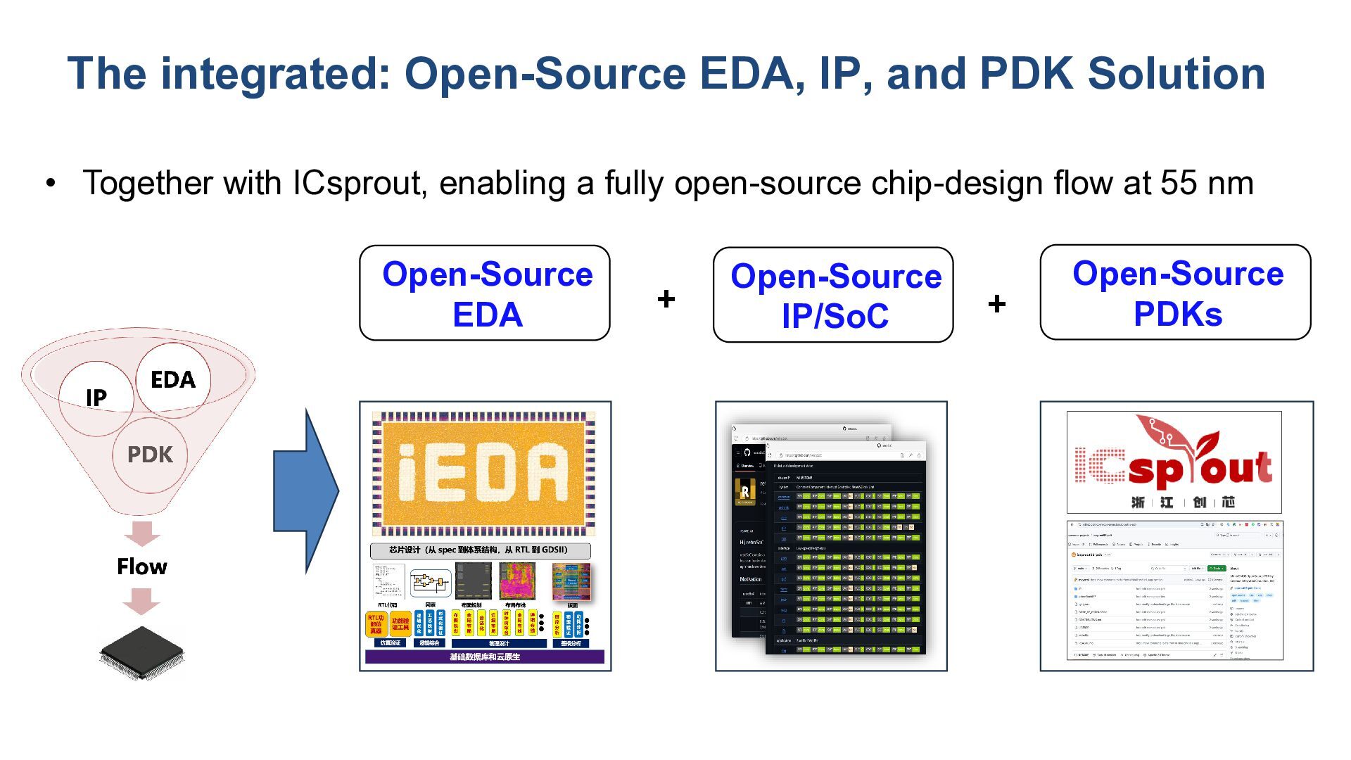
The integrated: Open-Source EDA, IP, and PDK Solution • Together
with ICsprout, enabling a fully open-source chip-design flow at 55 nm Open-Source EDA + Open-Source IP/SoC + Open-Source PDKs -
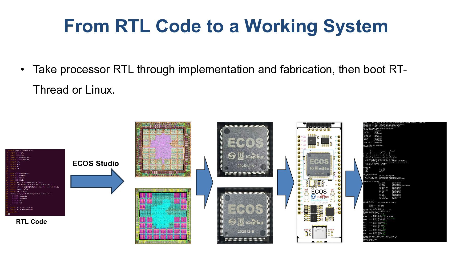
From RTL Code to a Working System • Take processor
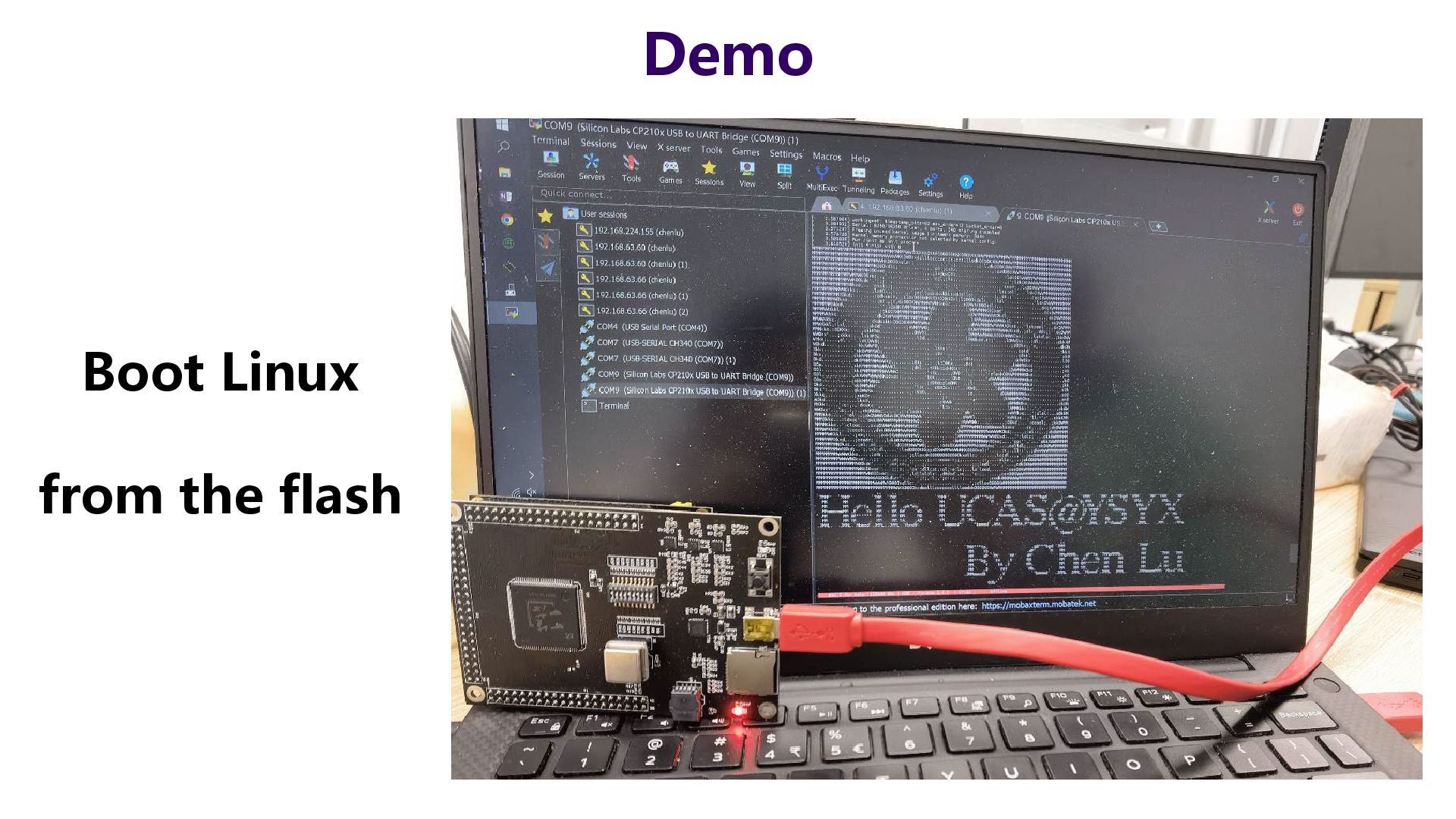
RTL through implementation and fabrication, then boot RTThread or Linux. ECOS Studio RTL Code -
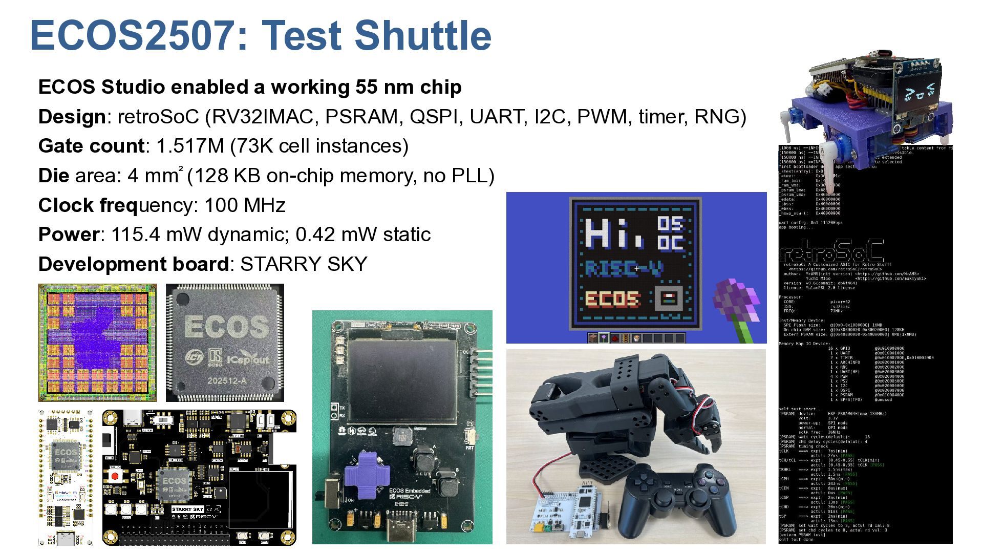
ECOS2507: Test Shuttle ECOS Studio enabled a working 55 nm
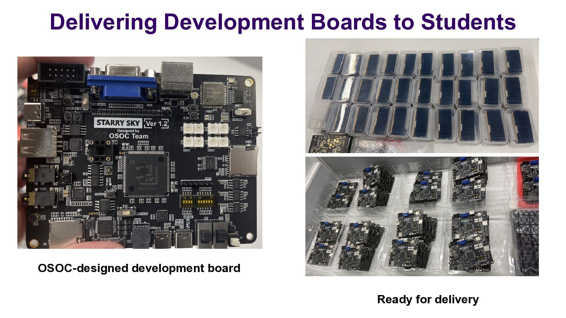
chip Design: retroSoC (RV32IMAC, PSRAM, QSPI, UART, I2C, PWM, timer, RNG) Gate count: 1.517M (73K cell instances) Die area: 4 mm² (128 KB on-chip memory, no PLL) Clock frequency: 100 MHz Power: 115.4 mW dynamic; 0.42 mW static Development board: STARRY SKY -
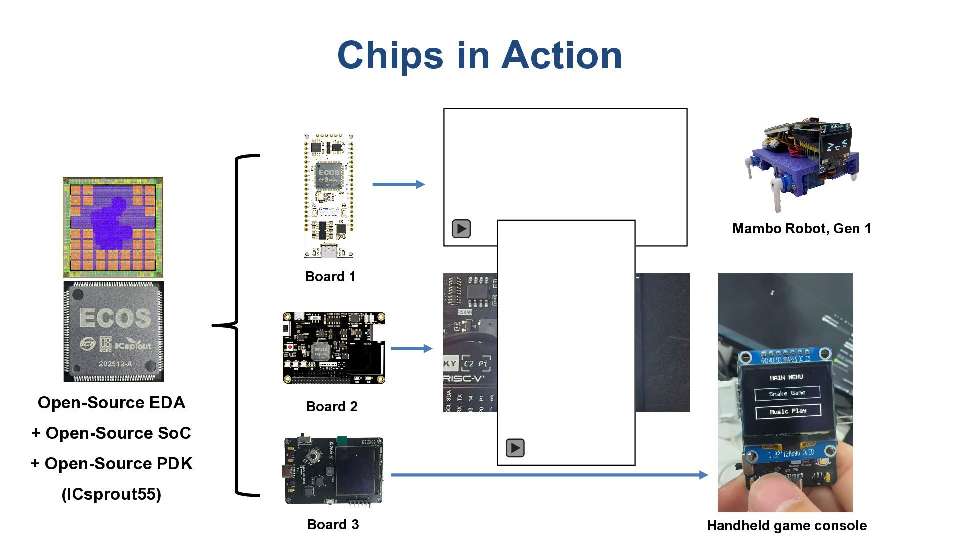
Chips in Action Mambo Robot, Gen 1 Board 1 Open-Source
EDA Board 2 + Open-Source SoC + Open-Source PDK (ICsprout55) Board 3 Handheld game console -
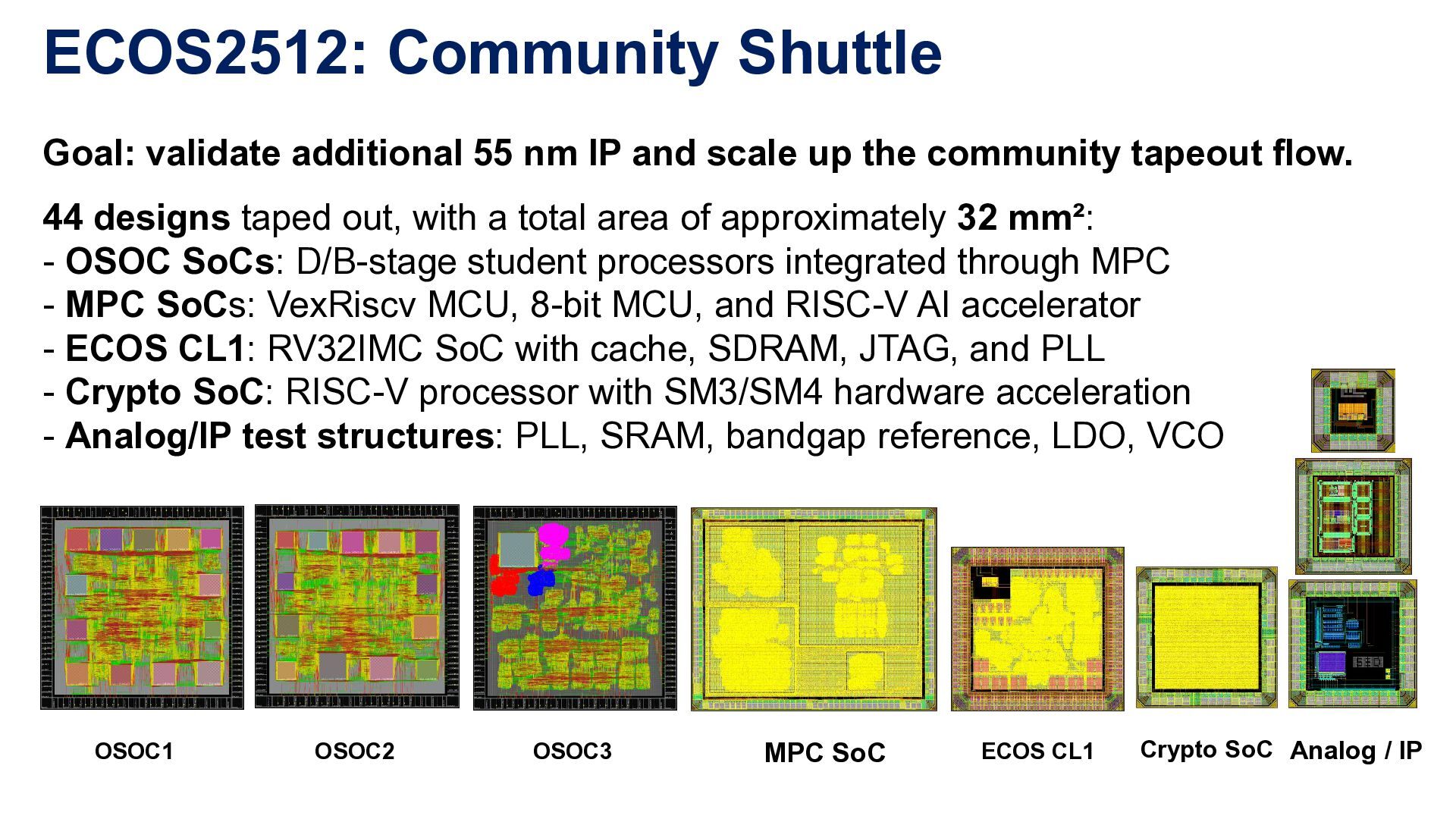
ECOS2512: Community Shuttle Goal: validate additional 55 nm IP and
scale up the community tapeout flow. 44 designs taped out, with a total area of approximately 32 mm²: - OSOC SoCs: D/B-stage student processors integrated through MPC - MPC SoCs: VexRiscv MCU, 8-bit MCU, and RISC-V AI accelerator - ECOS CL1: RV32IMC SoC with cache, SDRAM, JTAG, and PLL - Crypto SoC: RISC-V processor with SM3/SM4 hardware acceleration - Analog/IP test structures: PLL, SRAM, bandgap reference, LDO, VCO OSOC1 OSOC2 OSOC3 MPC SoC ECOS CL1 Crypto SoC Analog / IP -
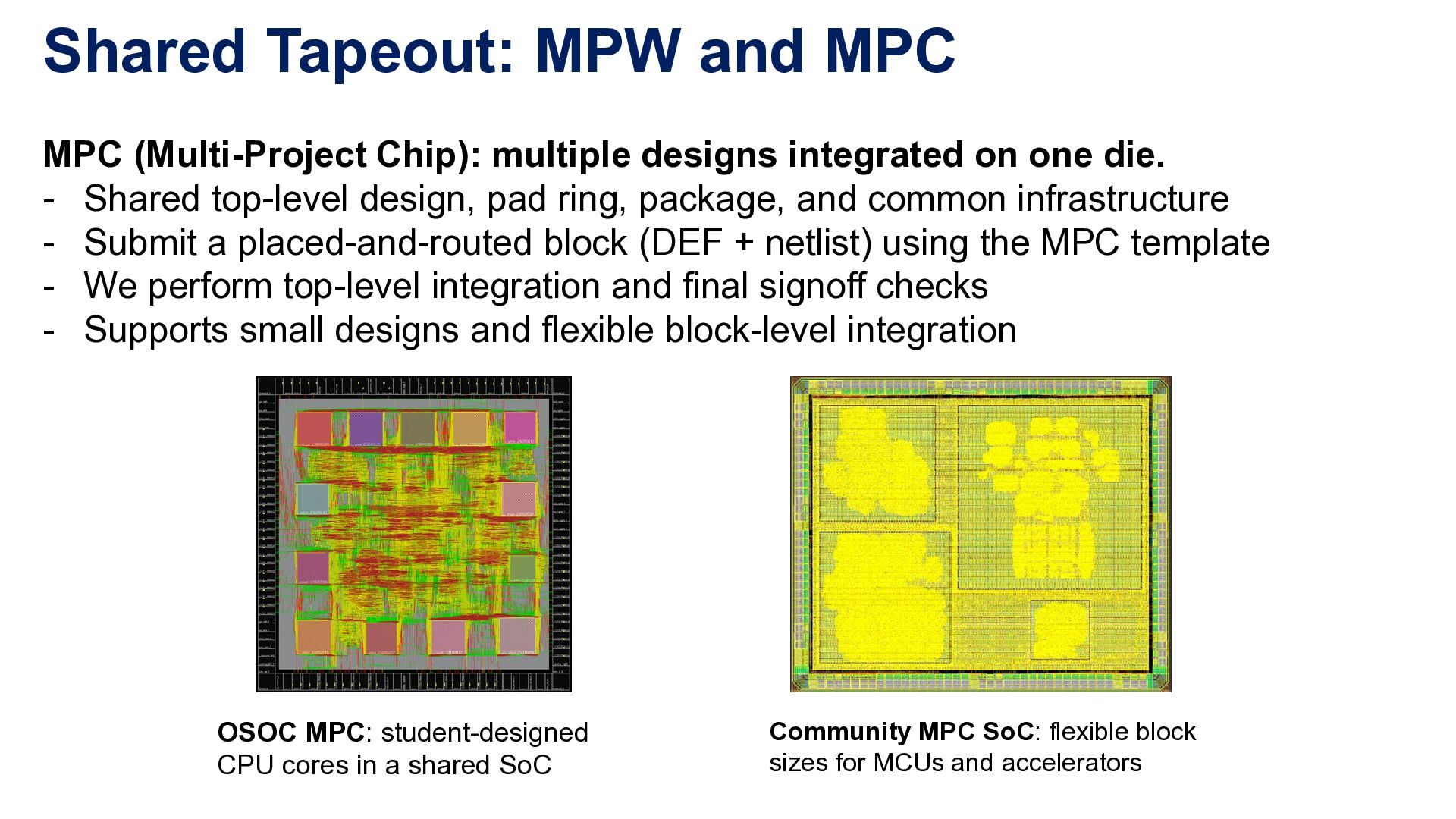
Shared Tapeout: MPW and MPC MPC (Multi-Project Chip): multiple designs
integrated on one die. - Shared top-level design, pad ring, package, and common infrastructure - Submit a placed-and-routed block (DEF + netlist) using the MPC template - We perform top-level integration and final signoff checks - Supports small designs and flexible block-level integration OSOC MPC: student-designed CPU cores in a shared SoC Community MPC SoC: flexible block sizes for MCUs and accelerators -
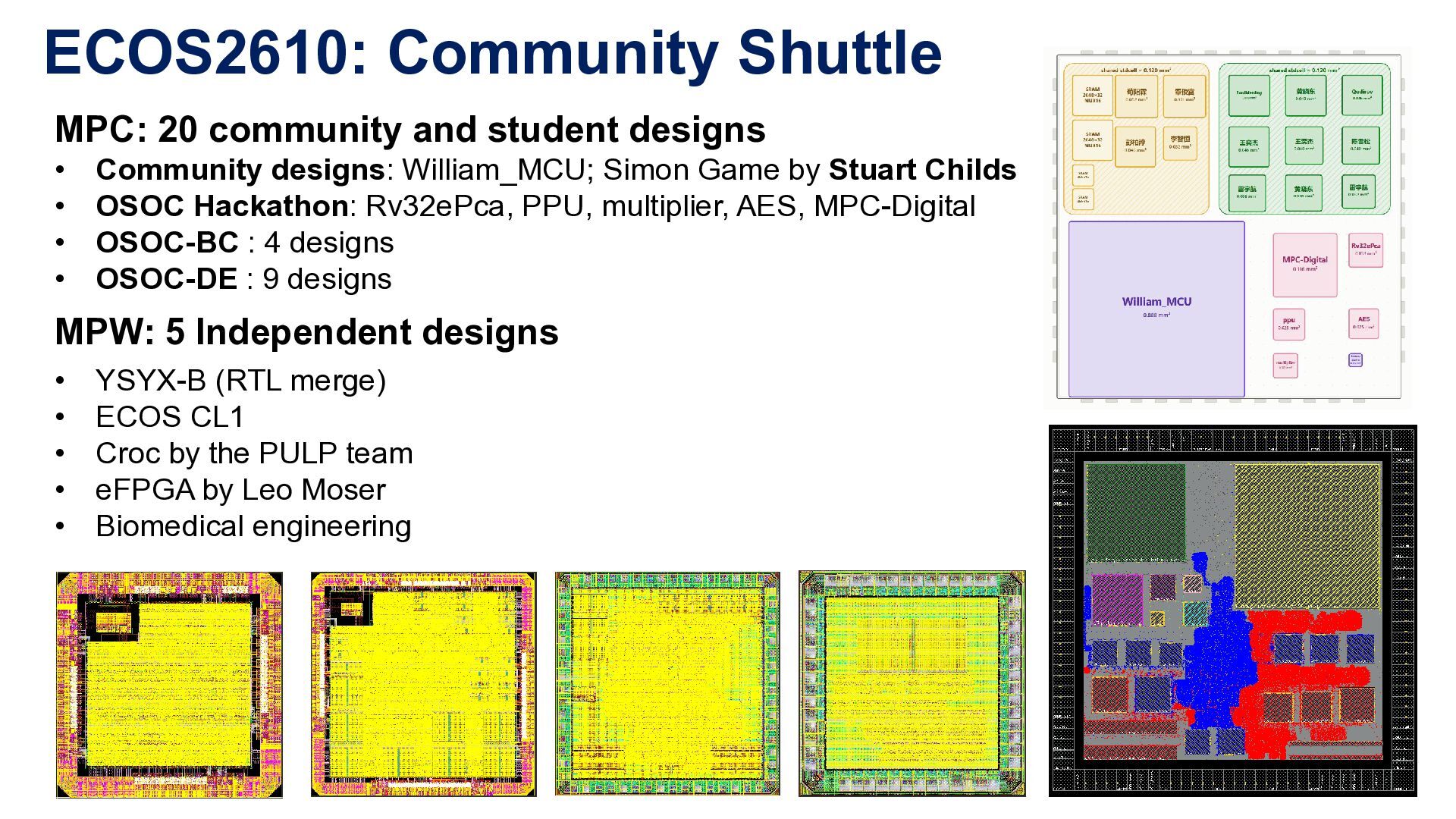
ECOS2610: Community Shuttle MPC: 20 community and student designs •
• • • Community designs: William_MCU; Simon Game by Stuart Childs OSOC Hackathon: Rv32ePca, PPU, multiplier, AES, MPC-Digital OSOC-BC : 4 designs OSOC-DE : 9 designs MPW: 5 Independent designs • • • • • YSYX-B (RTL merge) ECOS CL1 Croc by the PULP team eFPGA by Leo Moser Biomedical engineering -
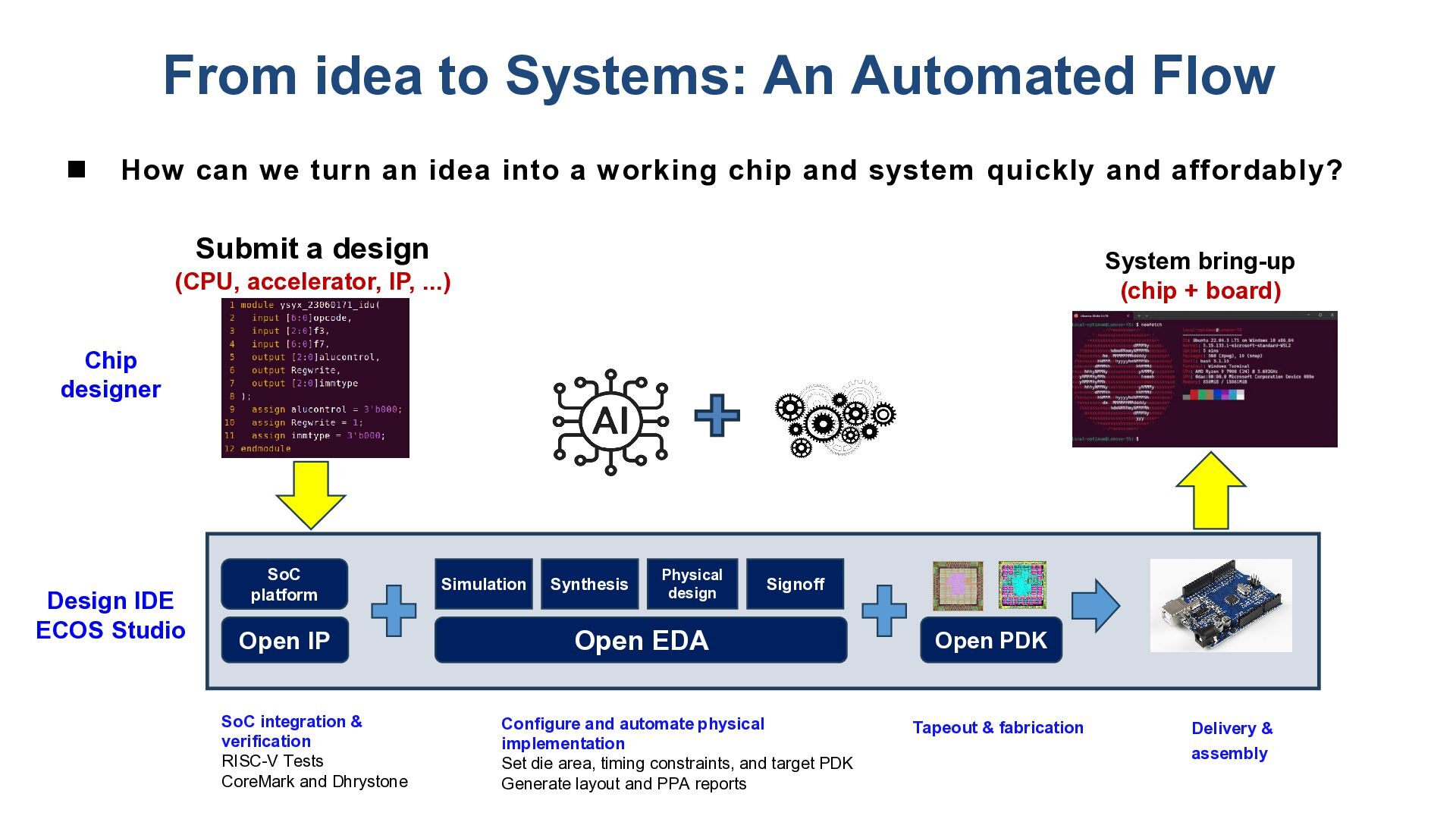
From idea to Systems: An Automated Flow How can
we turn an idea into a working chip and system quickly and affordably? Submit a design System bring-up (chip + board) (CPU, accelerator, IP, ...) Chip designer Design IDE ECOS Studio SoC platform Open IP SoC integration & verification RISC-V Tests CoreMark and Dhrystone Simulation Synthesis Physical design Signoff Open EDA Configure and automate physical implementation Set die area, timing constraints, and target PDK Generate layout and PPA reports Open PDK Tapeout & fabrication Delivery & assembly -
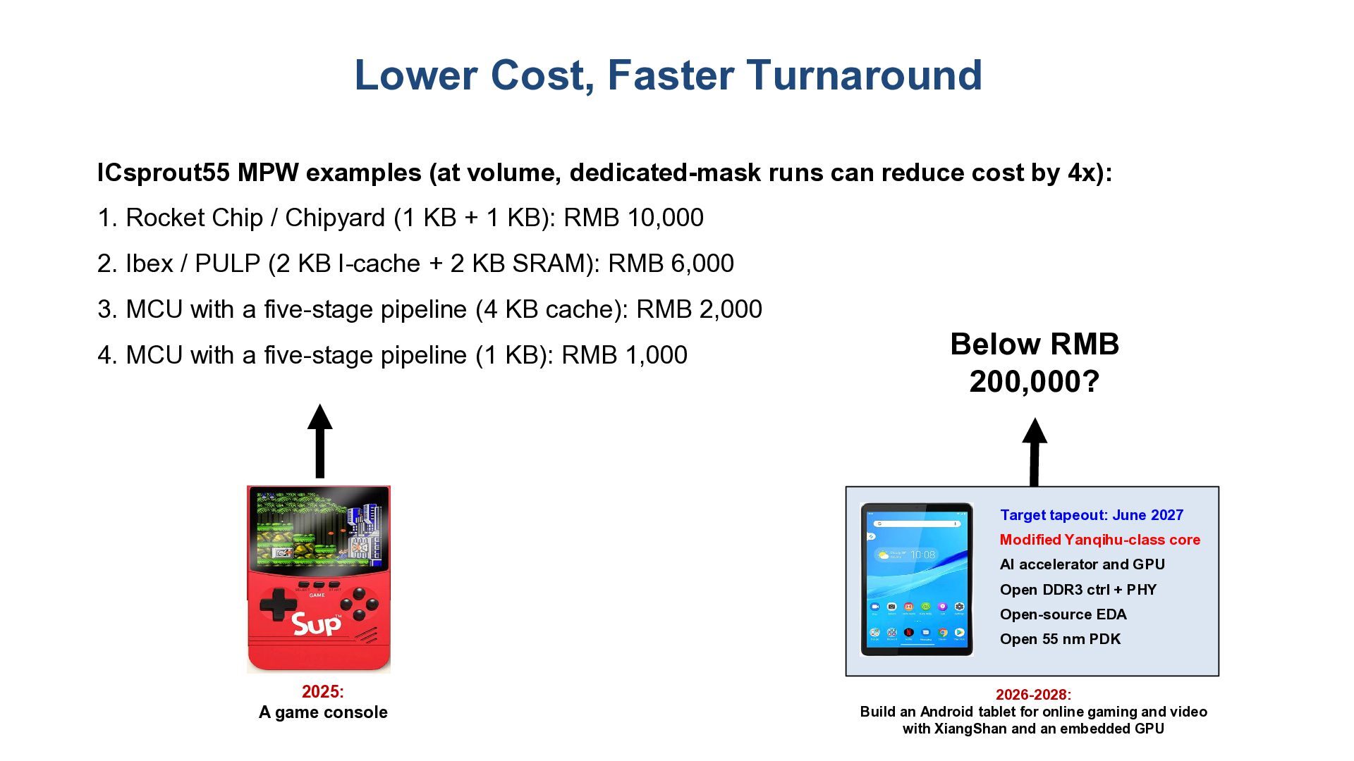
Lower Cost, Faster Turnaround ICsprout55 MPW examples (at volume, dedicated-mask
runs can reduce cost by 4x): 1. Rocket Chip / Chipyard (1 KB + 1 KB): RMB 10,000 2. Ibex / PULP (2 KB I-cache + 2 KB SRAM): RMB 6,000 3. MCU with a five-stage pipeline (4 KB cache): RMB 2,000 4. MCU with a five-stage pipeline (1 KB): RMB 1,000 Below RMB 200,000? Target tapeout: June 2027 Modified Yanqihu-class core AI accelerator and GPU Open DDR3 ctrl + PHY Open-source EDA Open 55 nm PDK 2025: A game console 2026-2028: Build an Android tablet for online gaming and video with XiangShan and an embedded GPU -
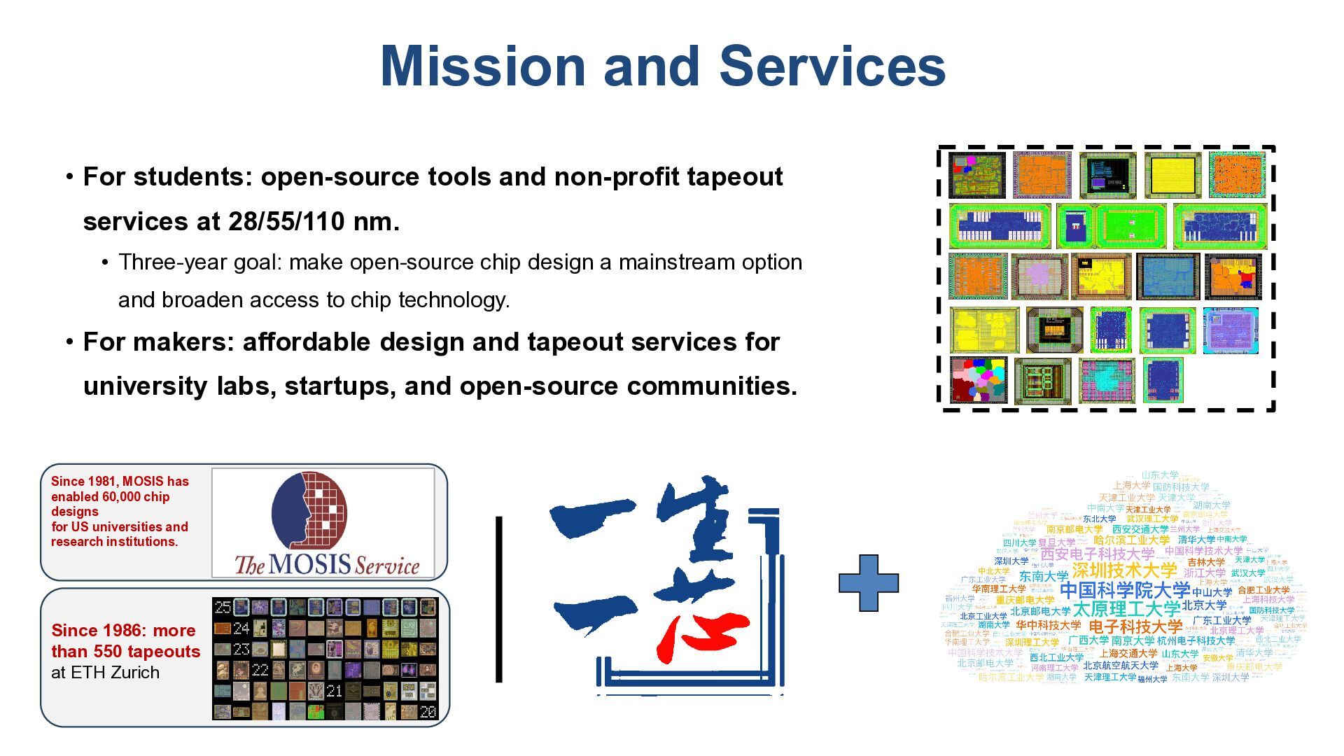
Mission and Services • For students: open-source tools and non-profit
tapeout services at 28/55/110 nm. • Three-year goal: make open-source chip design a mainstream option and broaden access to chip technology. • For makers: affordable design and tapeout services for university labs, startups, and open-source communities. Since 1981, MOSIS has enabled 60,000 chip designs for US universities and research institutions. Since 1986: more than 550 tapeouts at ETH Zurich -
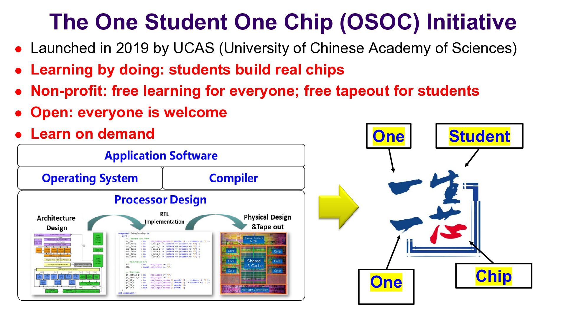
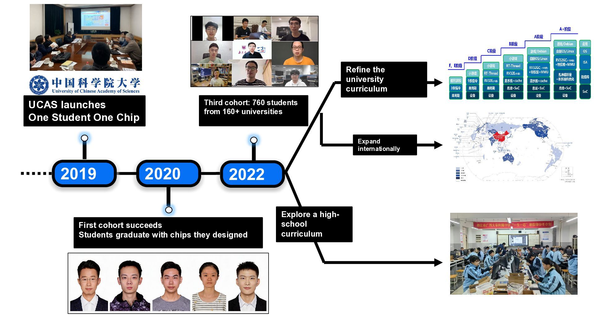
The One Student One Chip (OSOC) Initiative Launched in 2019
by UCAS (University of Chinese Academy of Sciences) Learning by doing: students build real chips Non-profit: free learning for everyone; free tapeout for students Open: everyone is welcome Learn on demand Student One One Chip -
Refine the university curriculum UCAS launches One Student One Chip
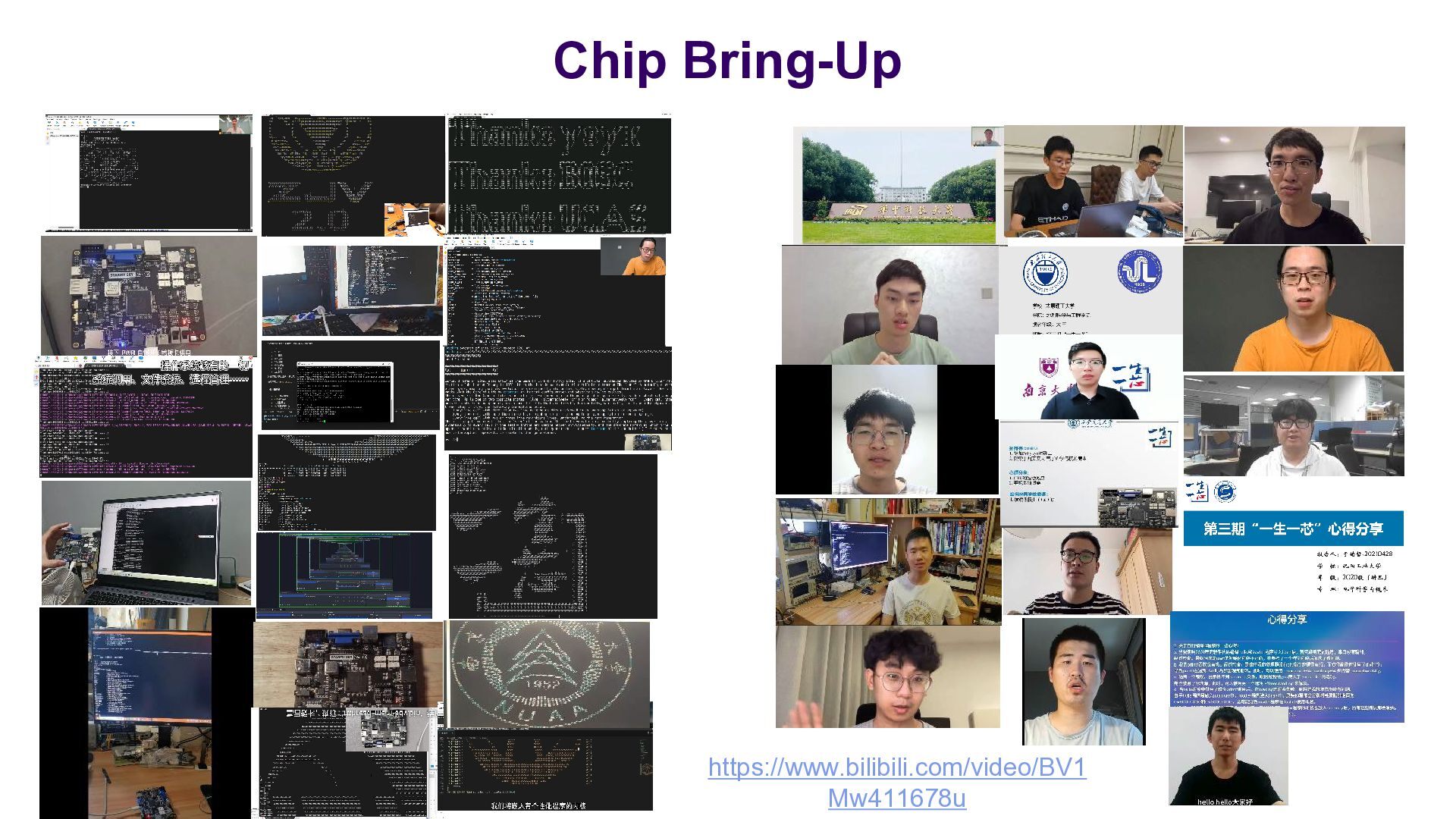
Third cohort: 760 students from 160+ universities Expand internationally 2019 2020 2022 First cohort succeeds Students graduate with chips they designed Explore a highschool curriculum -
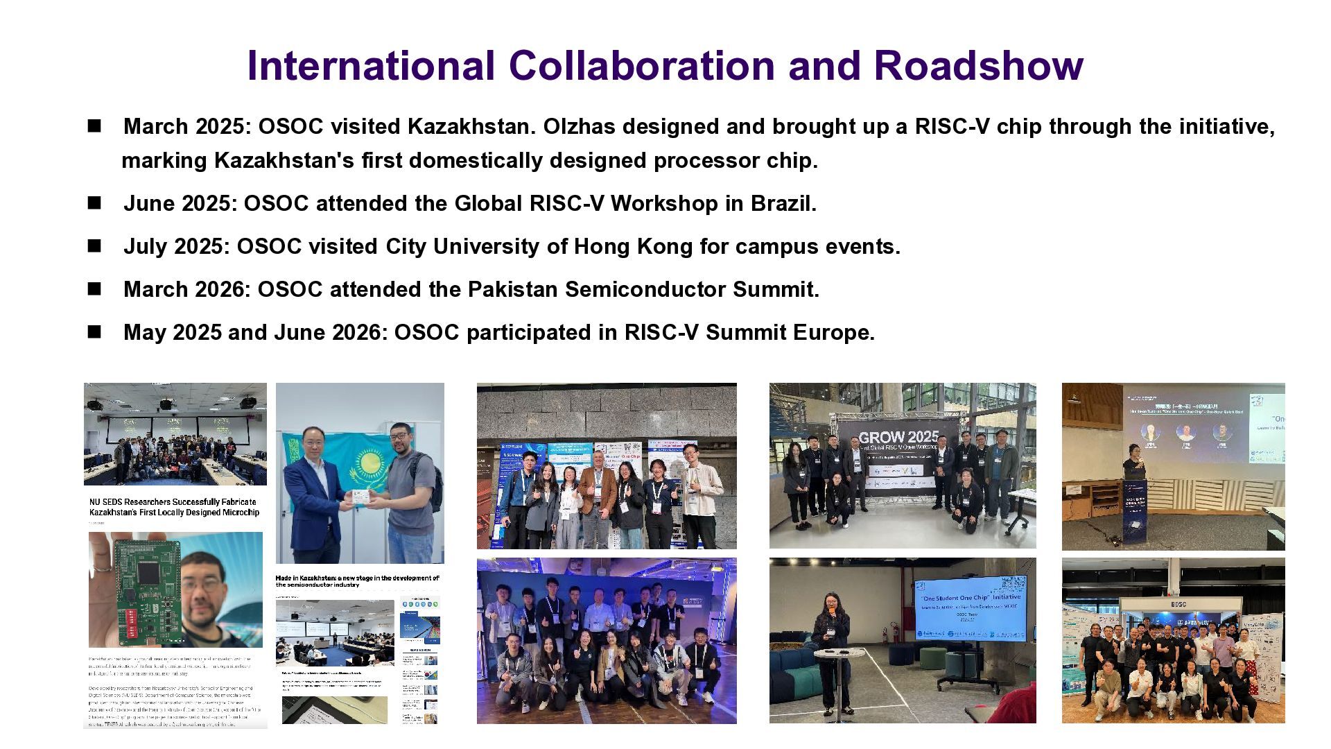
International Collaboration and Roadshow March 2025: OSOC visited Kazakhstan.
Olzhas designed and brought up a RISC-V chip through the initiative, marking Kazakhstan's first domestically designed processor chip. June 2025: OSOC attended the Global RISC-V Workshop in Brazil. July 2025: OSOC visited City University of Hong Kong for campus events. March 2026: OSOC attended the Pakistan Semiconductor Summit. May 2025 and June 2026: OSOC participated in RISC-V Summit Europe. -
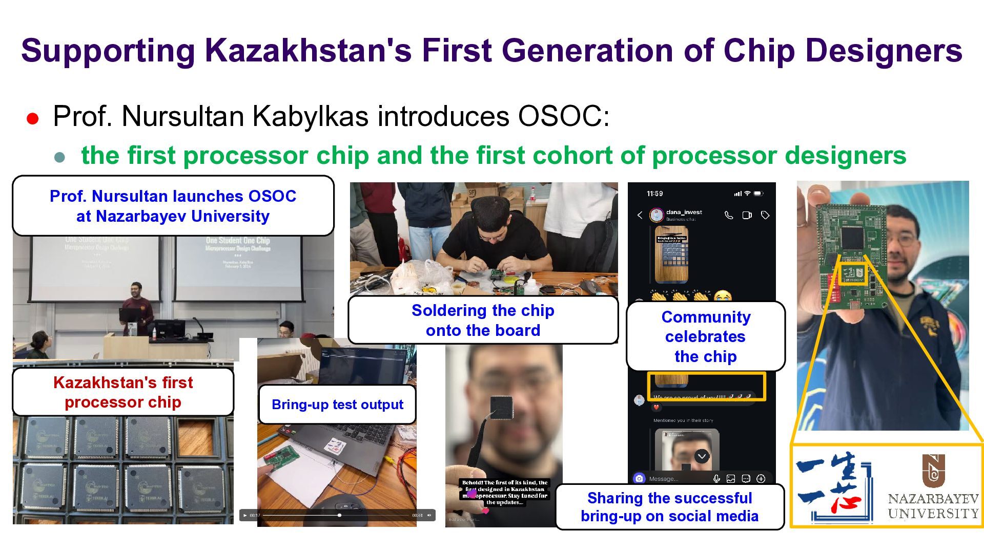
Supporting Kazakhstan's First Generation of Chip Designers Prof. Nursultan
Kabylkas introduces OSOC: the first processor chip and the first cohort of processor designers Prof. Nursultan launches OSOC at Nazarbayev University Soldering the chip onto the board Kazakhstan's first processor chip Community celebrates the chip Bring-up test output Sharing the successful bring-up on social media -
ECOS: An RTL-to-Chip Design Solution with Open-Source EDA, IP, and
PDKs ECOS Discord Channel Thank you Contacts Email: ECOS-ALL<[email protected]> GitHub: @openecos-projects Twitter: @openecos Wechat ECOS Team Institute of Computing Technology, Chinese Academy of Sciences 2026/11/11 Biwei Xie -
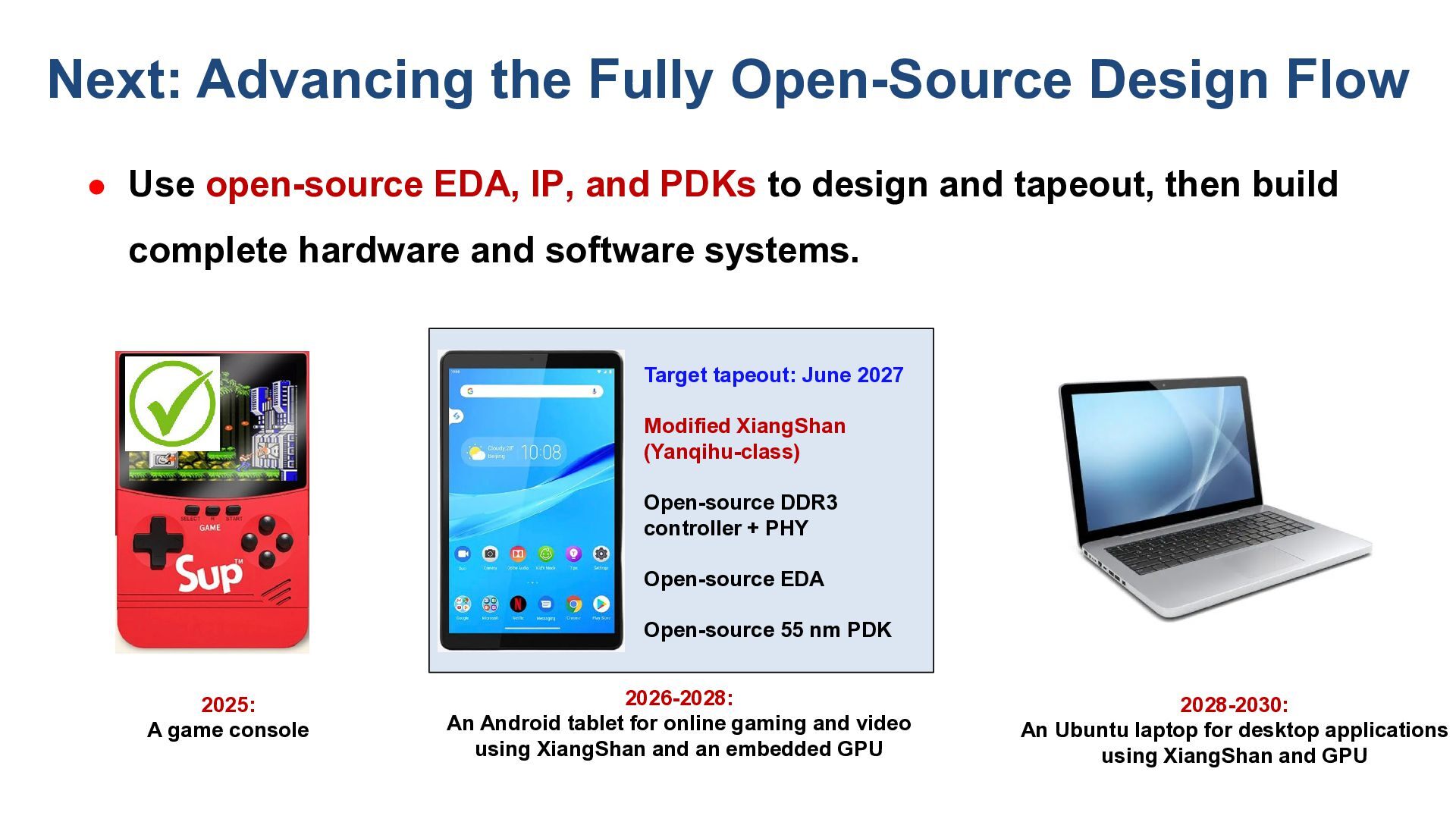
Next: Advancing the Fully Open-Source Design Flow Use open-source
EDA, IP, and PDKs to design and tapeout, then build complete hardware and software systems. Target tapeout: June 2027 Modified XiangShan (Yanqihu-class) Open-source DDR3 controller + PHY Open-source EDA Open-source 55 nm PDK 2025: A game console 2026-2028: An Android tablet for online gaming and video using XiangShan and an embedded GPU 2028-2030: An Ubuntu laptop for desktop applications using XiangShan and GPU -
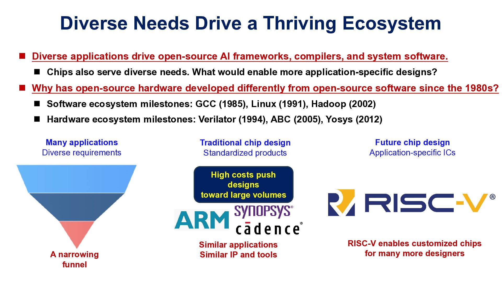
Diverse Needs Drive a Thriving Ecosystem Diverse applications drive
open-source AI frameworks, compilers, and system software. Chips also serve diverse needs. What would enable more application-specific designs? Why has open-source hardware developed differently from open-source software since the 1980s? Software ecosystem milestones: GCC (1985), Linux (1991), Hadoop (2002) Hardware ecosystem milestones: Verilator (1994), ABC (2005), Yosys (2012) Many applications Diverse requirements Traditional chip design Standardized products Future chip design Application-specific ICs High costs push designs toward large volumes A narrowing funnel Similar applications Similar IP and tools RISC-V enables customized chips for many more designers -
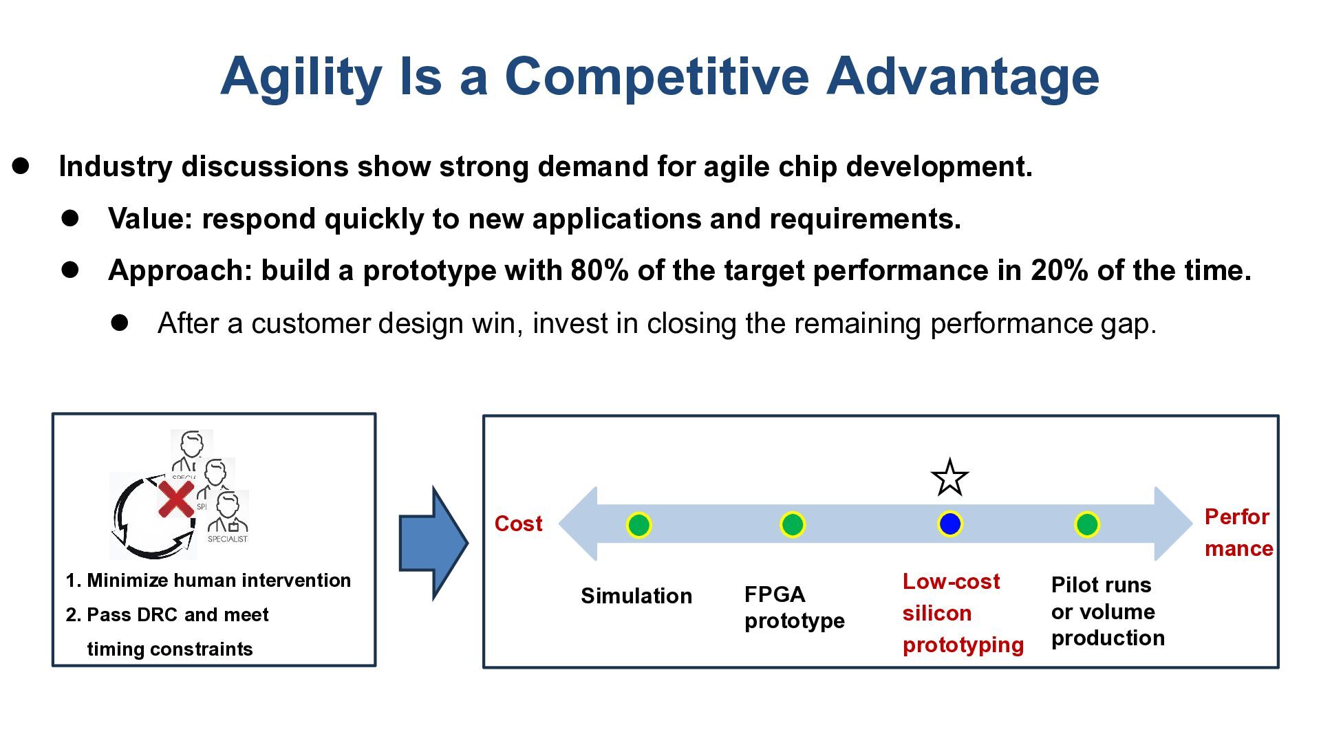
Agility Is a Competitive Advantage Industry discussions show strong
demand for agile chip development. Value: respond quickly to new applications and requirements. Approach: build a prototype with 80% of the target performance in 20% of the time. After a customer design win, invest in closing the remaining performance gap. Perfor mance Cost 1. Minimize human intervention 2. Pass DRC and meet timing constraints Simulation FPGA prototype Low-cost silicon prototyping Pilot runs or volume production -
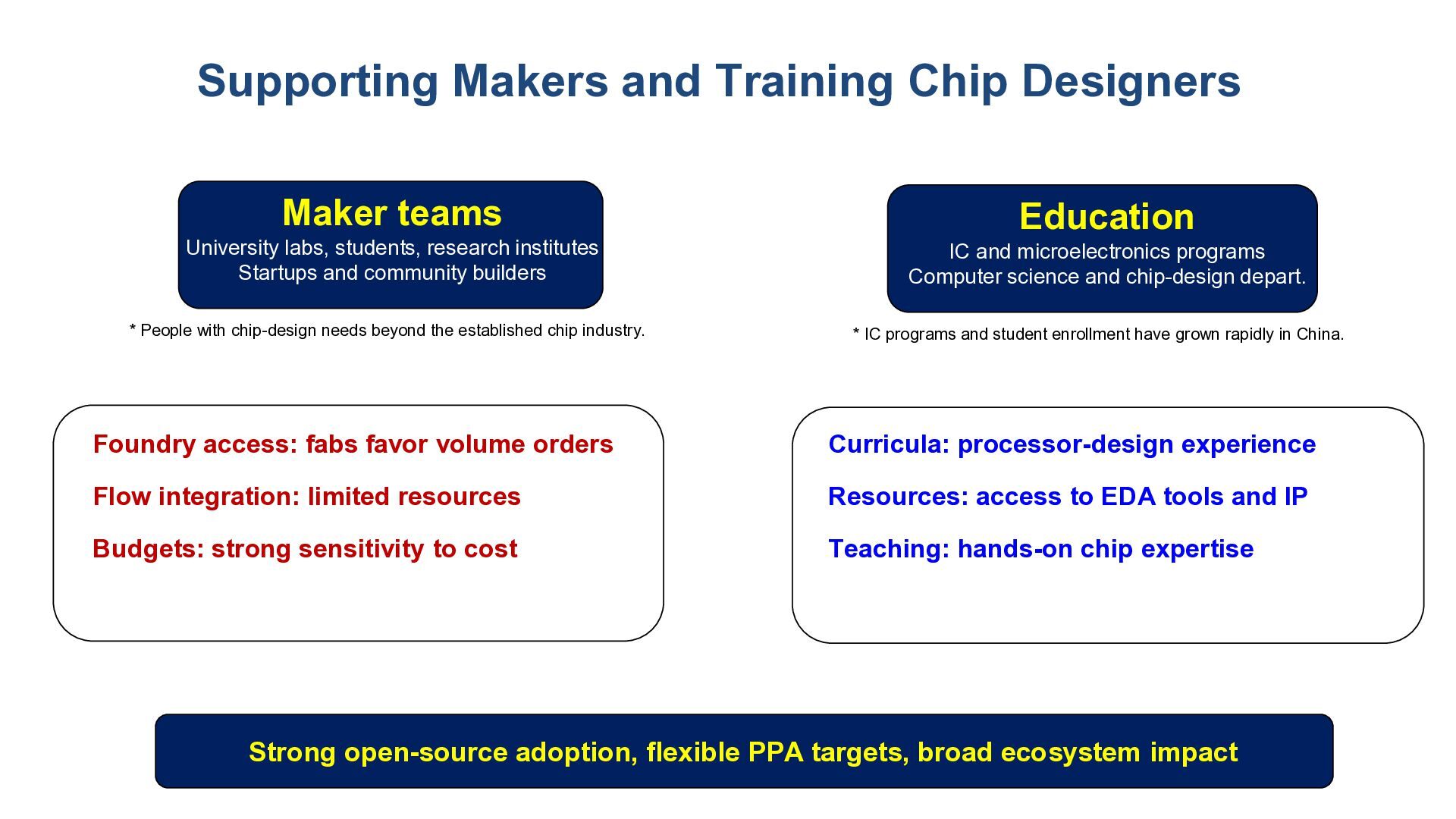
Supporting Makers and Training Chip Designers Maker teams Education University
labs, students, research institutes Startups and community builders IC and microelectronics programs Computer science and chip-design depart. * People with chip-design needs beyond the established chip industry. * IC programs and student enrollment have grown rapidly in China. Foundry access: fabs favor volume orders Curricula: processor-design experience Flow integration: limited resources Resources: access to EDA tools and IP Budgets: strong sensitivity to cost Teaching: hands-on chip expertise Strong open-source adoption, flexible PPA targets, broad ecosystem impact -
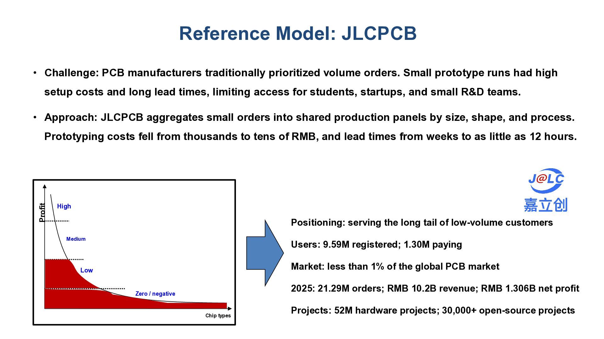
Reference Model: JLCPCB • Challenge: PCB manufacturers traditionally prioritized volume
orders. Small prototype runs had high setup costs and long lead times, limiting access for students, startups, and small R&D teams. • Approach: JLCPCB aggregates small orders into shared production panels by size, shape, and process. Profit Prototyping costs fell from thousands to tens of RMB, and lead times from weeks to as little as 12 hours. High Positioning: serving the long tail of low-volume customers Medium Users: 9.59M registered; 1.30M paying Market: less than 1% of the global PCB market Low 2025: 21.29M orders; RMB 10.2B revenue; RMB 1.306B net profit Zero / negative Chip types Projects: 52M hardware projects; 30,000+ open-source projects
 takasumasakazu
 bluesmoon
 codingconduct
 mojombo
 aleyda
 tammyeverts
 morganepeng
 inesmontani
 popppiees
 nwiizo
 eileencodes
 lcolladotor