Upgrade to Pro — share decks privately, control downloads, hide ads and more …

J601_lec01

 J601_lec01

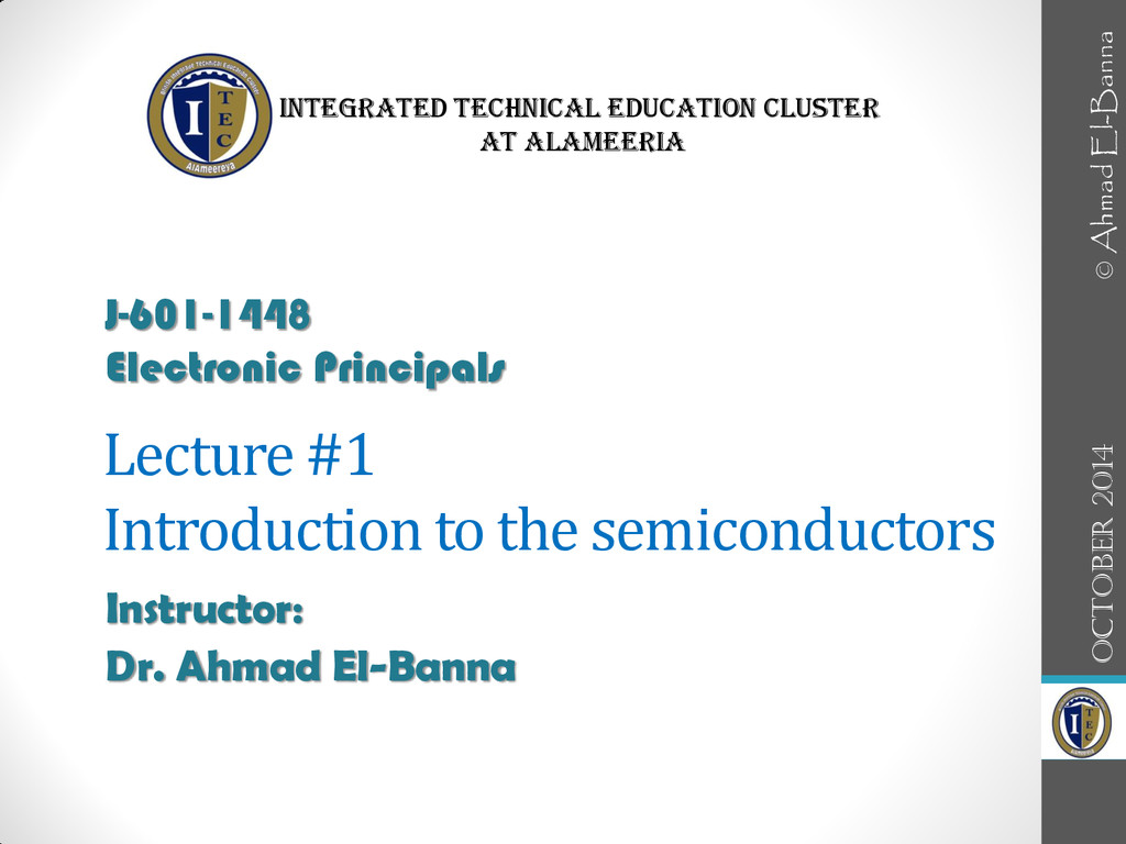
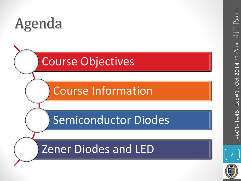
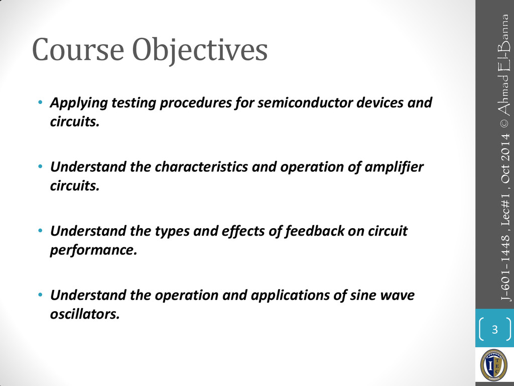
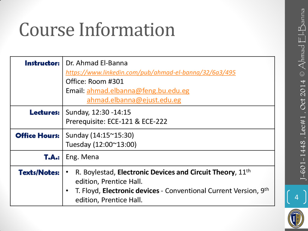
5th Year, Integrated Technical Education Cluster AlAmeeria‎
lec#1, Electronic Principals
(over 2 weeks, 12 Oct & 19 Oct)

Ahmad El-Banna

October 12, 2014
Tweet

More Decks by Ahmad El-Banna

Other Decks in Education

Transcript

  1. Lecture #1 Introduction to the semiconductors Instructor: Dr. Ahmad El-Banna

    October 2014 J-601-1448 Electronic Principals Integrated Technical Education Cluster At AlAmeeria‎ © Ahmad El-Banna
  2. Agenda Course Objectives Course Information Semiconductor Diodes Zener Diodes and

    LED 2 J-601-1448 , Lec#1 , Oct 2014 © Ahmad El-Banna
  3. Course Objectives • Applying testing procedures for semiconductor devices and

    circuits. • Understand the characteristics and operation of amplifier circuits. • Understand the types and effects of feedback on circuit performance. • Understand the operation and applications of sine wave oscillators. 3 J-601-1448 , Lec#1 , Oct 2014 © Ahmad El-Banna
  4. Course Information Instructor: Dr. Ahmad El-Banna https://www.linkedin.com/pub/ahmad-el-banna/32/6a3/495 Office: Room #301

    Email: [email protected] [email protected] Lectures: Sunday, 12:30 -14:15 Prerequisite: ECE-121 & ECE-222 Office Hours: Sunday (14:15~15:30) Tuesday (12:00~13:00) T.A.: Eng. Mena Texts/Notes: • R. Boylestad, Electronic Devices and Circuit Theory, 11th edition, Prentice Hall. • T. Floyd, Electronic devices - Conventional Current Version, 9th edition, Prentice Hall. 4 J-601-1448 , Lec#1 , Oct 2014 © Ahmad El-Banna
  5. Lectures List 5 • Weeks 1:6 • Applying testing procedures

    for semiconductor devices and circuits. • Weeks 7:10 • Understand the characteristics and operation of amplifier circuits. • Weeks 11:12 • Understand the types and effects of feedback on circuit performance. • Weeks 13:14 • Understand the operation and applications of sine wave oscillators. • Week 15 • Course close and feedback J-601-1448 , Lec#1 , Oct 2014 © Ahmad El-Banna
  6. Semiconductor Materials • Semiconductors are a special class of elements

    having a conductivity between that of a good conductor and that of an insulator. • The three semiconductors used most frequently in the construction of electronic devices are Ge, Si, and GaAs. 7 J-601-1448 , Lec#1 , Oct 2014 © Ahmad El-Banna
  7. N-type and P-type materials • A semiconductor material that has

    been subjected to the doping process is called an extrinsic material. • N-type: • Diffused impurities with five valence electrons are called donor atoms. • In an n-type material the electron is called the majority carrier and the hole the minority carrier. • P-type: • The diffused impurities with three valence electrons are called acceptor atoms. • In a p-type material the hole is the majority carrier and the electron is the minority carrier. 8 J-601-1448 , Lec#1 , Oct 2014 © Ahmad El-Banna
  8. Semiconductor Diode • No applied bias: • This region of

    uncovered positive and negative ions is called the depletion region due to the “depletion” of free carriers in the region. • In the absence of an applied bias across a semiconductor diode, the net flow of charge in one direction is zero. • Reverse-Bias condition: • The current that exists under reverse-bias conditions is called the reverse saturation current and is represented by Is . • Forward-Bias condition: • A forward-bias or “on” condition is established by applying the positive potential to the p -type material and the negative potential to the n -type material 9 J-601-1448 , Lec#1 , Oct 2014 © Ahmad El-Banna
  9. Semiconductor Diode.. 10 J-601-1448 , Lec#1 , Oct 2014 •

    The defined direction of conventional current for the positive voltage region matches the arrowhead in the diode symbol. • The actual reverse saturation current of a commercially available diode will normally be measurably larger than that appearing as the reverse saturation current in Shockley’s equation. • The maximum reverse-bias potential that can be applied before entering the break-down region is called the peak inverse voltage (referred to simply as the PIV rating) or the peak reverse voltage (denoted the PRV rating). © Ahmad El-Banna
  10. Ge/Si/GaAs & Temperature Effect 11 J-601-1448 , Lec#1 , Oct

    2014 • In the forward-bias region the characteristics of a silicon diode shift to the left at a rate of 2.5 mV per centigrade degree increase in temperature. • In the reverse-bias region the reverse current of a silicon diode doubles for every 10°C rise in temperature. • The reverse breakdown voltage of a semiconductor diode will increase or decrease with temperature. © Ahmad El-Banna
  11. Ideal vs. Practical • The semiconductor diode behaves in a

    manner similar to a mechanical switch in that it can control whether current will flow between its two terminals. • The semiconductor diode is different from a mechanical switch in the sense that when the switch is closed it will only permit current to flow in one direction. • At any current level on the vertical line, the voltage across the ideal diode is 0 V and the resistance is 0 . • Because the current is 0 mA anywhere on the horizontal line, the resistance is considered to be infinite ohms (an open-circuit) at any point on the axis. 12 J-601-1448 , Lec#1 , Oct 2014 © Ahmad El-Banna
  12. Resistance Levels • DC or Static Resistance: • In general,

    therefore, the higher the current through a diode, the lower is the dc resistance level. • the dc resistance of a diode is independent of the shape of the characteristic in the region surrounding the point of interest. • AC or Dynamic Resistance: • If a sinusoidal rather than a dc input is applied, then the varying input will move the instantaneous operating point up and down a region of the characteristics and thus defines a specific change in current and voltage. • A straight line drawn tangent to the curve through the Q –point will define a particular change in voltage and current that can be used to determine the ac or dynamic resistance for this region of the diode characteristics. • In general, the lower the Q-point of operation (smaller current or lower voltage), the higher is the ac resistance. 13 J-601-1448 , Lec#1 , Oct 2014 © Ahmad El-Banna
  13. Resistance Levels.. • Average AC resistance • If the input

    signal is sufficiently large to produce a broad swing, the resistance associated with the device for this region is called the average ac resistance. • The average ac resistance is, by definition, the resistance determined by a straight line drawn between the two intersections established by the maximum and minimum values of input voltage. 14 J-601-1448 , Lec#1 , Oct 2014 • Summary table © Ahmad El-Banna
  14. Diode Equivalent Circuit • An equivalent circuit is a combination

    of elements properly chosen to best represent the actual terminal characteristics of a device or system in a particular operating region. • If the characteristics or specification sheet for a diode is not available the resistance rav can be approximated by the ac resistance rd . 15 J-601-1448 , Lec#1 , Oct 2014 © Ahmad El-Banna
  15. Transition and Diffusion Capacitance • Every electronic or electrical device

    is frequency sensitive. • As we approach high frequencies, stray capacitive and inductive effects start to play a role and will affect the total impedance level of the element. • the transition capacitance CT , barriers, or depletion region capacitance, is the predominant capacitive effect in the reverse-bias region whereas the diffusion capacitance is the predominant capacitive effect in the forward-bias region. • the diffusion capacitance CD a capacitance effect directly dependent on the rate at which charge is injected into the regions just outside the depletion region. 16 J-601-1448 , Lec#1 , Oct 2014 © Ahmad El-Banna
  16. Reverse Recovery Time 17 J-601-1448 , Lec#1 , Oct 2014

    © Ahmad El-Banna • The period of time ts (storage time) required for the minority carriers to return to their majority-carrier state in the opposite material. • When this storage phase has passed, the current will be reduced in level to that associated with the non conduction state. This second period of time is denoted by tt (transition interval). • The reverse recovery time is the sum of these two intervals: trr =ts + tt • Most commercially available switching diodes have a trr in the range of a few nanoseconds to 1 us.
  17. Diode Specification Sheets They include: 1. The forward voltage VF

    (at a specified current and temperature) 2. The maximum forward current IF (at a specified temperature) 3. The reverse saturation current IR (at a specified voltage and temperature) 4. The reverse-voltage rating [PIV or PRV or V(BR), where BR comes from the term “breakdown” (at a specified temperature)] 5. The maximum power dissipation level at a particular temperature 6. Capacitance levels 7. Reverse recovery time trr 8. Operating temperature range 18 J-601-1448 , Lec#1 , Oct 2014 © Ahmad El-Banna
  18. Diode Testing • Diode Checking Function 21 J-601-1448 , Lec#1

    , Oct 2014 • Ohmmeter Testing • Curve Tracer © Ahmad El-Banna
  19. Zener Diodes 23 J-601-1448 , Lec#1 , Oct 2014 •

    The characteristic drops in an almost vertical manner at a reverse-bias potential denoted VZ . • The fact that the curve drops down and away from the horizontal axis rather than up and away for the positive- VD region reveals that the current in the Zener region has a direction opposite to that of a forward-biased diode. © Ahmad El-Banna
  20. LED • In Si and Ge diodes the greater percentage

    of the energy converted during recombination at the junction is dissipated in the form of heat within the structure, and the emitted light is insignificant. • Diodes constructed of GaAs emit light in the infrared (invisible) zone during the recombination process at the p–n junction. 24 J-601-1448 , Lec#1 , Oct 2014 © Ahmad El-Banna
  21. LED.. • The frequency spectrum for infrared light extends from

    about 100 THz (T = tera = 1012 ) to 400 THz, with the visible light spectrum extending from about 400 to 750 THz. • The response of the average human eye extends from about 350 nm to 800 nm with a peak near 550 nm. • The wavelength and frequency of light of a specific color are directly related to the energy band gap of the material. • A first step in the production of a compound semiconductor that can be used to generate light is to come up with a combination of elements that will generate the desired energy band gap. 25 J-601-1448 , Lec#1 , Oct 2014 © Ahmad El-Banna
  22. LED… 26 J-601-1448 , Lec#1 , Oct 2014 • The

    light intensity of an LED will increase with forward current until a point of saturation arrives where any further increase in current will not effectively increase the level of illumination. • One of the major concerns when using an LED is the reverse-bias breakdown voltage, which is typically between 3V and 5V. • For many years the only colors available were green, yellow, orange, and red, permitting the use of the average values of VF =2 V and IF =20 mA for obtaining an approximate operating level. © Ahmad El-Banna
  23. • For more details, refer to: • Chapter 1, Electronic

    Devices and Circuits, Boylestad. • The lecture is available online at: • https://speakerdeck.com/ahmad_elbanna • For inquires, send to: • [email protected][email protected] 28 J-601-1448 , Lec#1 , Oct 2014 © Ahmad El-Banna