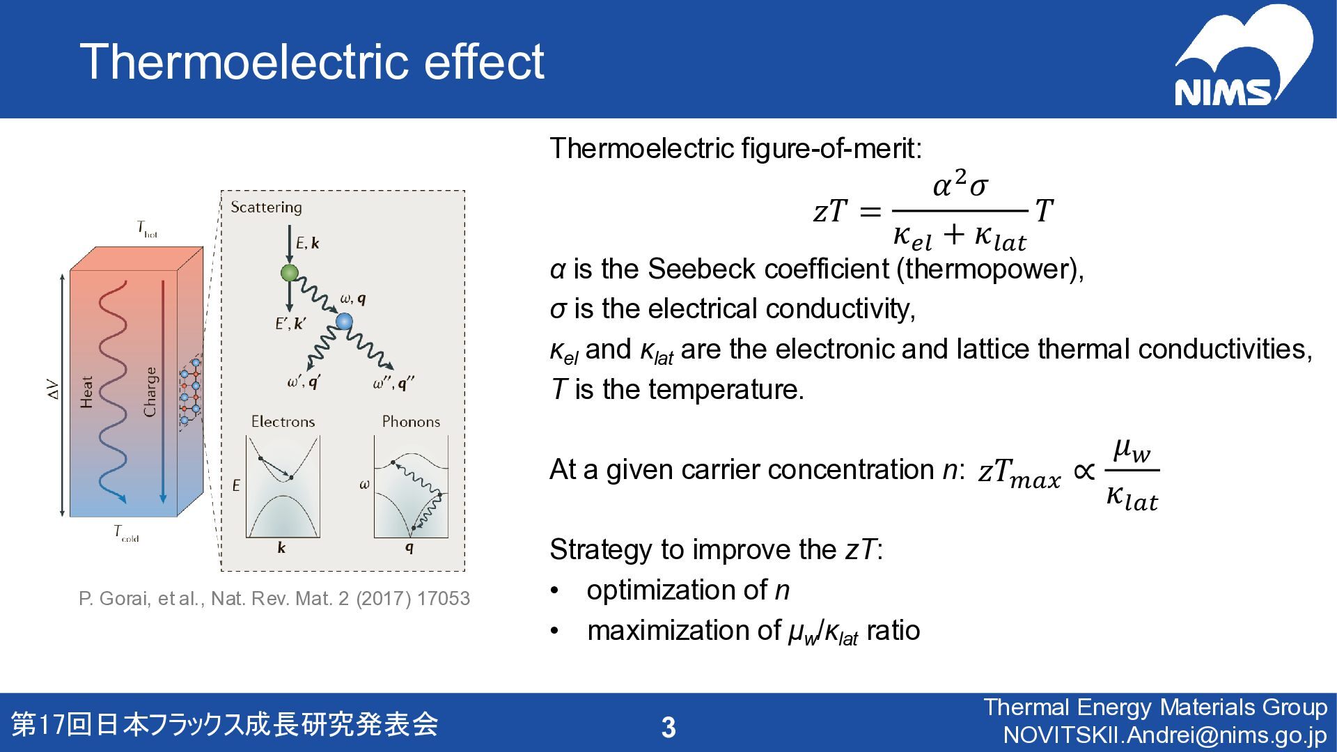
coefficient (thermopower), σ is the electrical conductivity, κel and κlat are the electronic and lattice thermal conductivities, T is the temperature. At a given carrier concentration n: Strategy to improve the zT: • optimization of n • maximization of μw /κlat ratio Thermal Energy Materials Group [email protected] P. Gorai, et al., Nat. Rev. Mat. 2 (2017) 17053 𝑧𝑇 = 𝛼2𝜎 𝜅𝑒𝑙 + 𝜅𝑙𝑎𝑡 𝑇 𝑧𝑇𝑚𝑎𝑥 ∝ 𝜇𝑤 𝜅𝑙𝑎𝑡
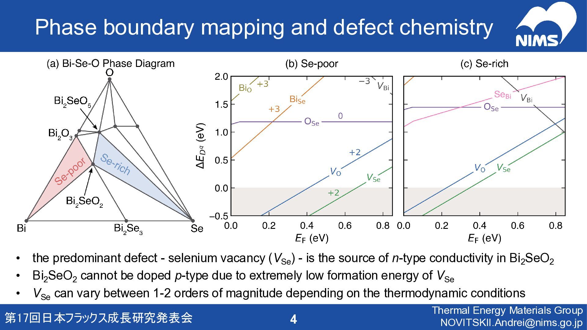
defect - selenium vacancy (VSe ) - is the source of n-type conductivity in Bi2 SeO2 • Bi2 SeO2 cannot be doped p-type due to extremely low formation energy of VSe • VSe can vary between 1-2 orders of magnitude depending on the thermodynamic conditions 第17回日本フラックス成長研究発表会 Thermal Energy Materials Group [email protected]
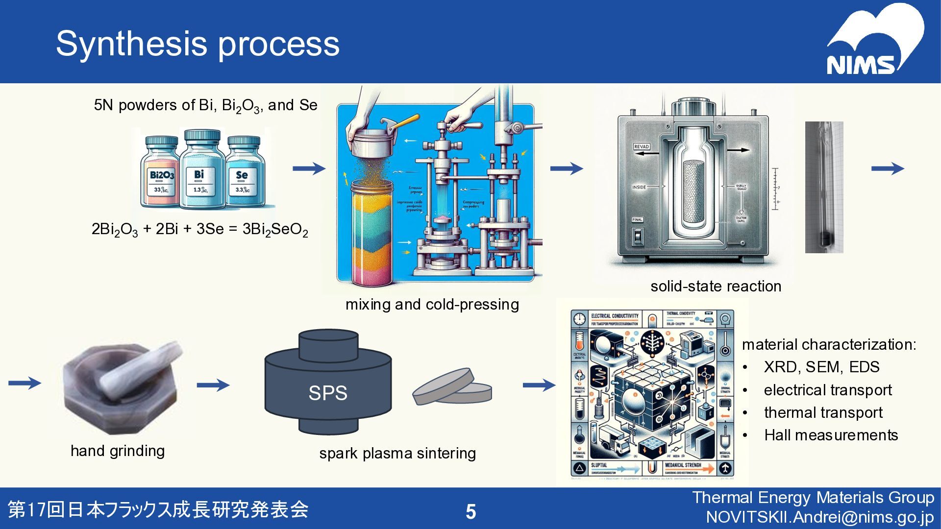
grinding 第17回日本フラックス成長研究発表会 Thermal Energy Materials Group [email protected] 5N powders of Bi, Bi2 O3 , and Se solid-state reaction material characterization: • XRD, SEM, EDS • electrical transport • thermal transport • Hall measurements SPS 2Bi2 O3 + 2Bi + 3Se = 3Bi2 SeO2
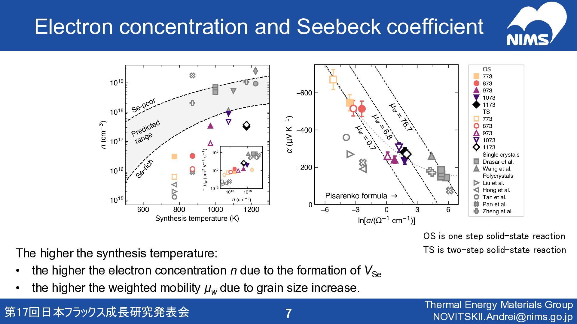
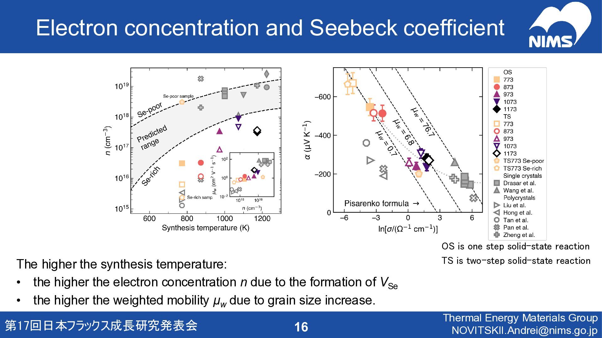
Group [email protected] The higher the synthesis temperature: • the higher the electron concentration n due to the formation of VSe • the higher the weighted mobility μw due to grain size increase. OS is one step solid-state reaction TS is two-step solid-state reaction
higher the synthesis temperature: • the higher the electrical conductivity due to increase in n and μ • the lattice thermal conductivity. OS is one step solid-state reaction TS is two-step solid-state reaction
theory and experiment to demonstrate that the TE performance in n-type Bi2 SeO2 can be improved by systematically controlling defect formation with synthesis conditions: • The electron concentration increases by elevating synthesis temperature (TSSR ), leading to an increase in α2σ power factor. • Furthermore, samples with higher VSe concentrations exhibit suppressed thermal conductivity due to point defect-induced phonon scattering and microstructural changes. • Cumulatively, defect engineering yields a fourfold improvement of the zT in self-doped Bi2 SeO2 , ultimately reaching 0.25 at 773 K. • This study underscores TSSR as a rational, accessible experimental parameter for controlling defect formation in Bi2 SeO2 . OS is one step solid-state reaction TS is two-step solid-state reaction
from the JST Mirai JPMJMI19A1. 第17回日本フラックス成長研究発表会 先生: 森 孝雄 Supervisor: Mori Takao Prashun Gorai Michael Toriyama G. Jeffrey Snyder Illia Serhiienko Thermal Energy Materials Group [email protected]
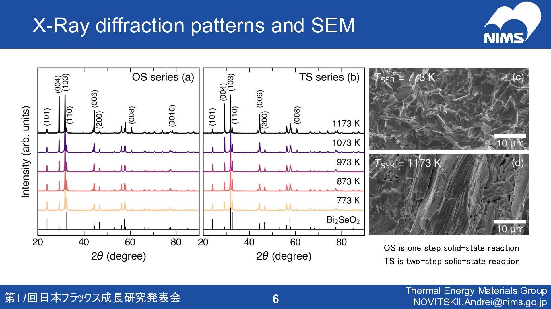
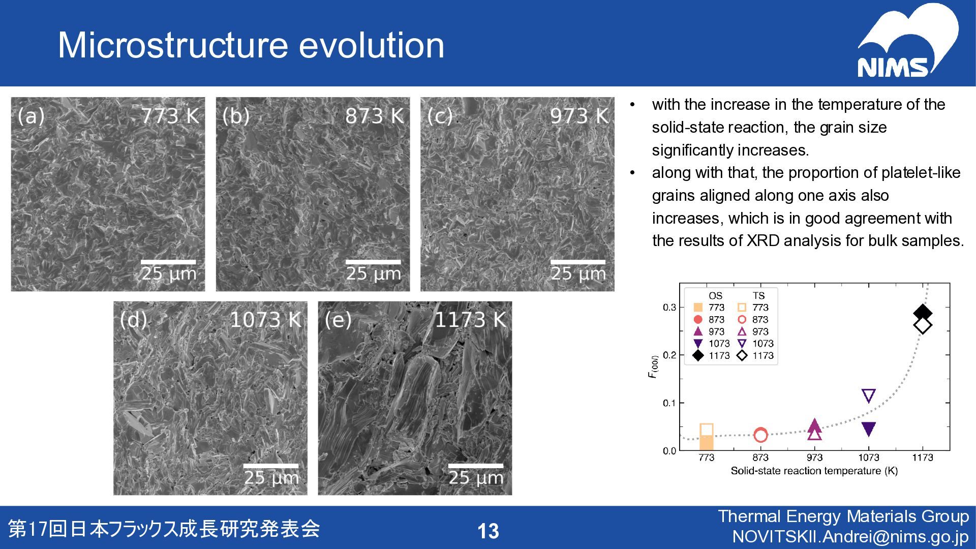
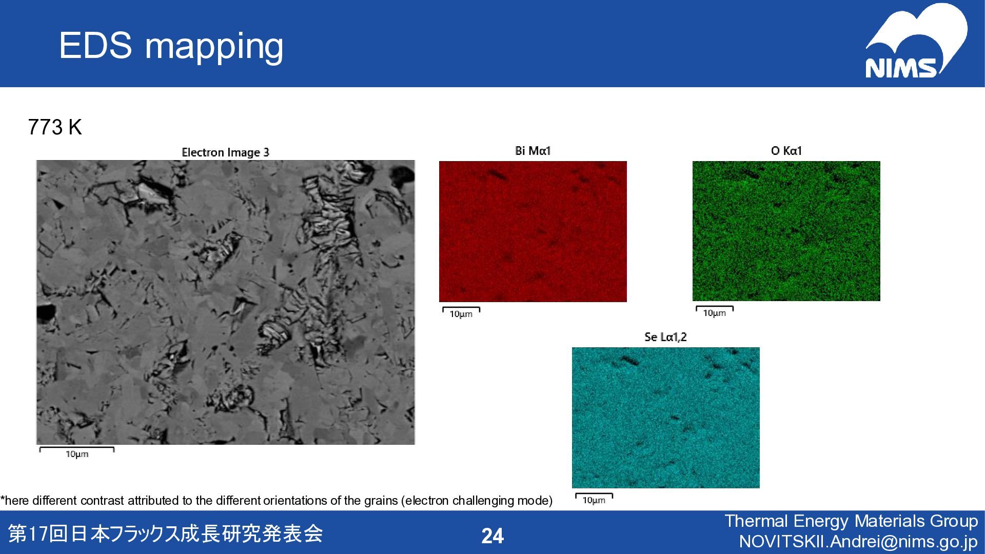
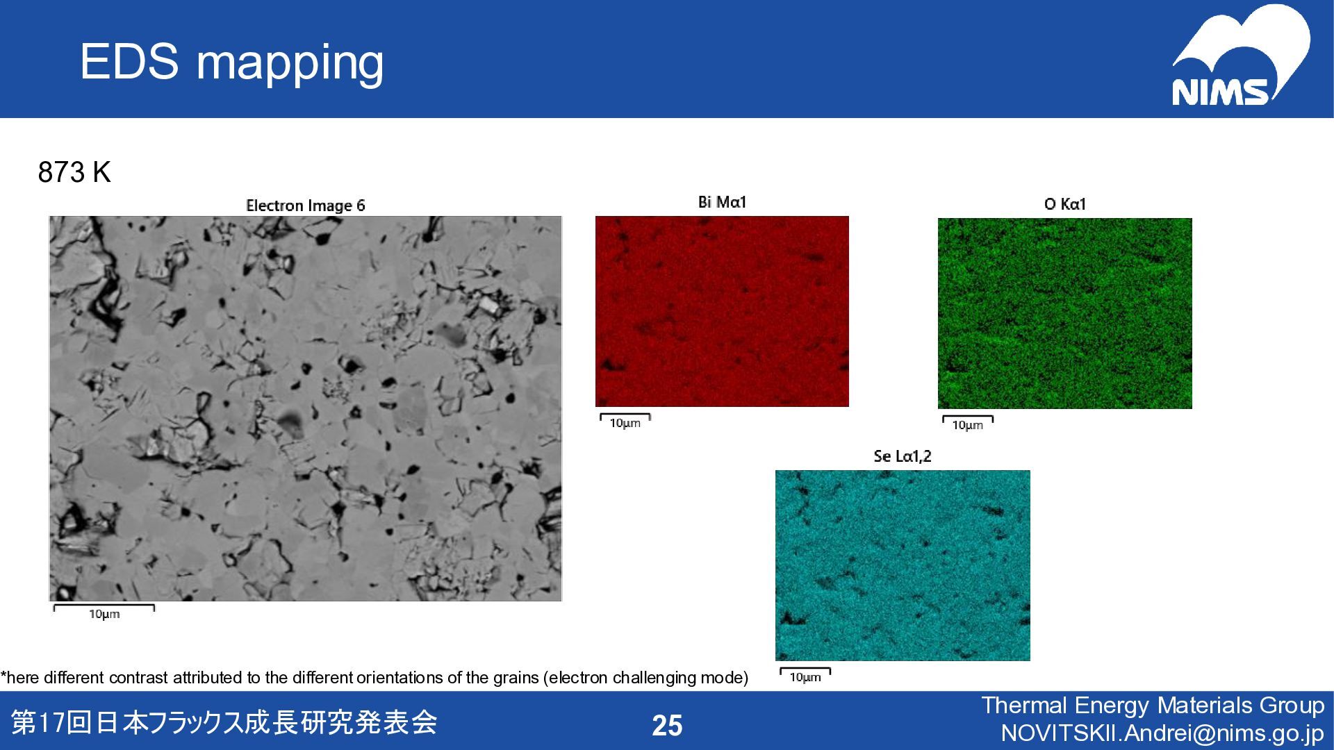
of the solid-state reaction, the grain size significantly increases. • along with that, the proportion of platelet-like grains aligned along one axis also increases, which is in good agreement with the results of XRD analysis for bulk samples. 第17回日本フラックス成長研究発表会 Thermal Energy Materials Group [email protected]
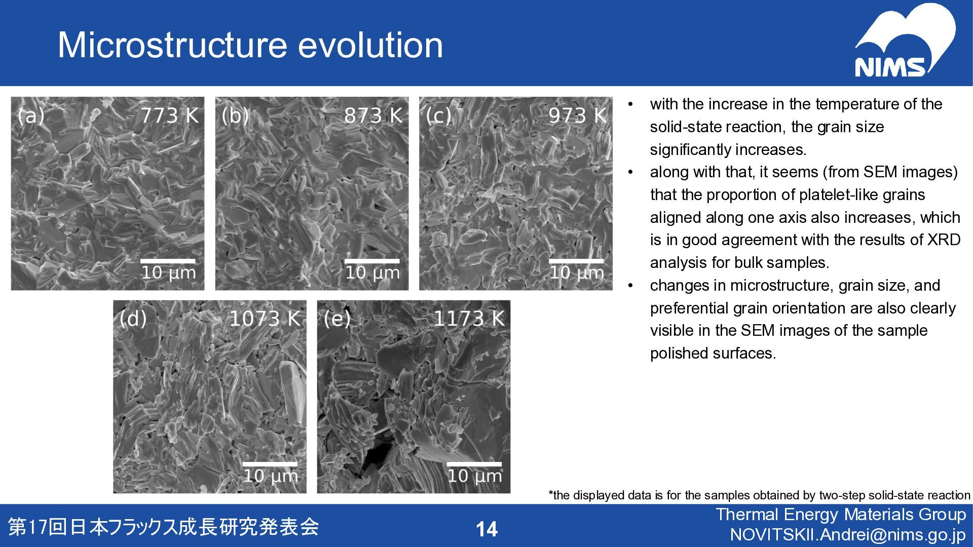
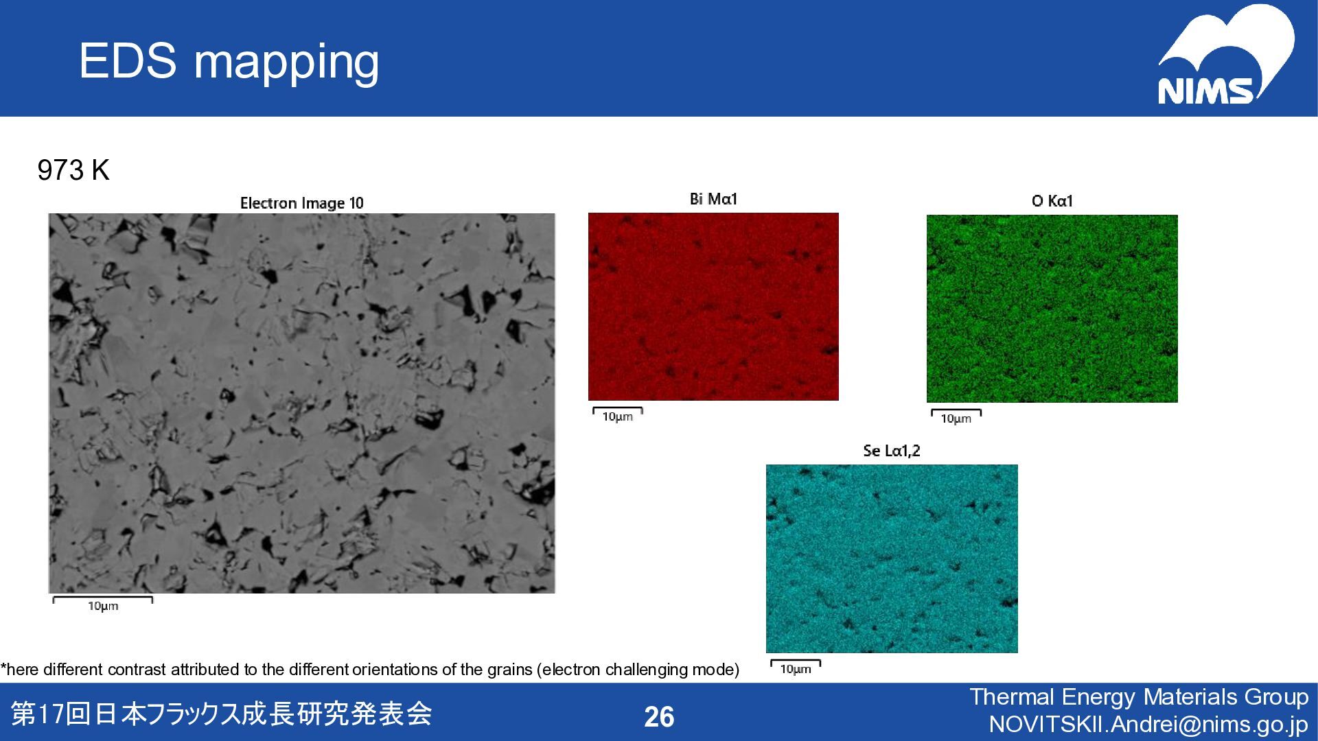
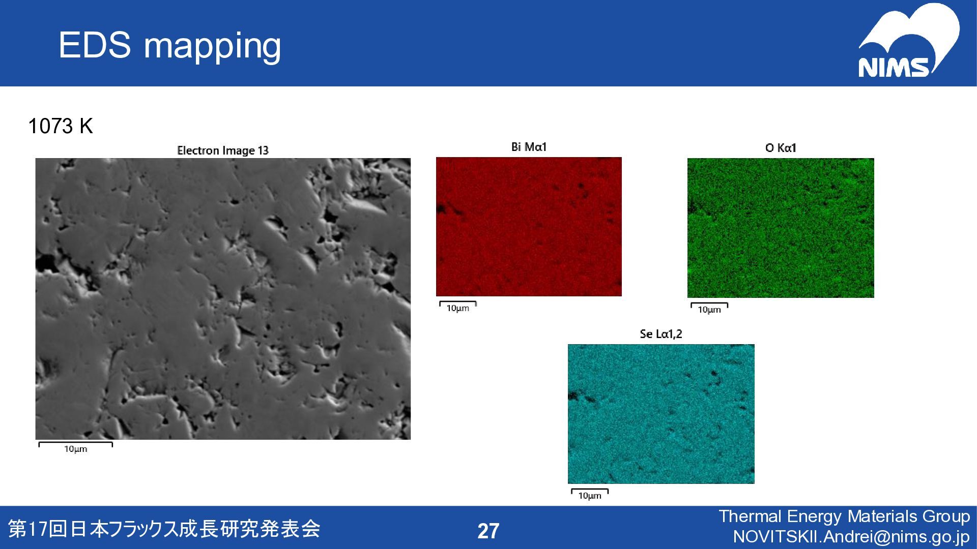
obtained by two-step solid-state reaction • with the increase in the temperature of the solid-state reaction, the grain size significantly increases. • along with that, it seems (from SEM images) that the proportion of platelet-like grains aligned along one axis also increases, which is in good agreement with the results of XRD analysis for bulk samples. • changes in microstructure, grain size, and preferential grain orientation are also clearly visible in the SEM images of the sample polished surfaces. 第17回日本フラックス成長研究発表会 Thermal Energy Materials Group [email protected]
Group [email protected] The higher the synthesis temperature: • the higher the electron concentration n due to the formation of VSe • the higher the weighted mobility μw due to grain size increase. OS is one step solid-state reaction TS is two-step solid-state reaction
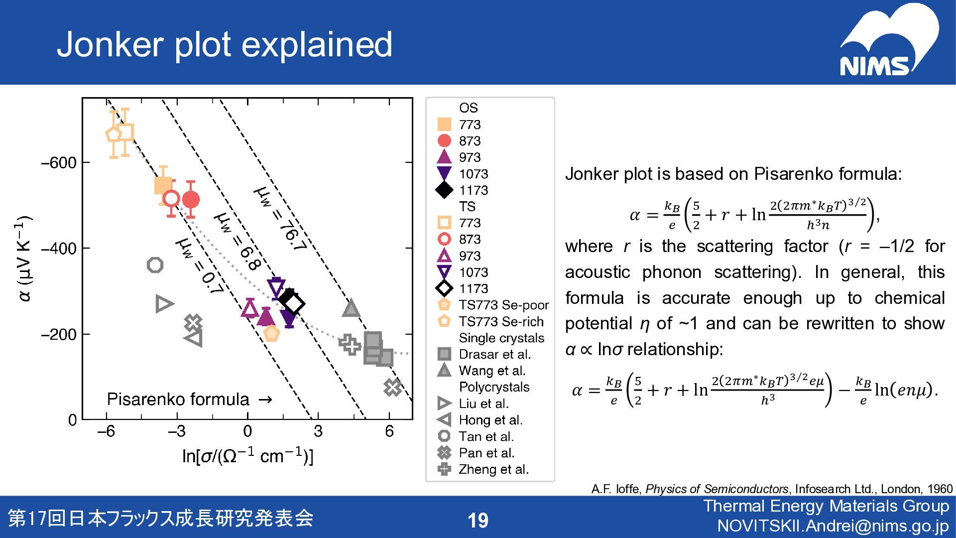
formula: 𝛼 = 𝑘𝐵 𝑒 5 2 + 𝑟 + ln 2 2𝜋𝑚∗𝑘𝐵𝑇 Τ 3 2 ℎ3𝑛 , where r is the scattering factor (r = –1/2 for acoustic phonon scattering). In general, this formula is accurate enough up to chemical potential η of ~1 and can be rewritten to show α ∝ lnσ relationship: 𝛼 = 𝑘𝐵 𝑒 5 2 + 𝑟 + ln 2 2𝜋𝑚∗𝑘𝐵𝑇 Τ 3 2𝑒𝜇 ℎ3 − 𝑘𝐵 𝑒 ln 𝑒𝑛𝜇 . A.F. Ioffe, Physics of Semiconductors, Infosearch Ltd., London, 1960 第17回日本フラックス成長研究発表会 Thermal Energy Materials Group [email protected]
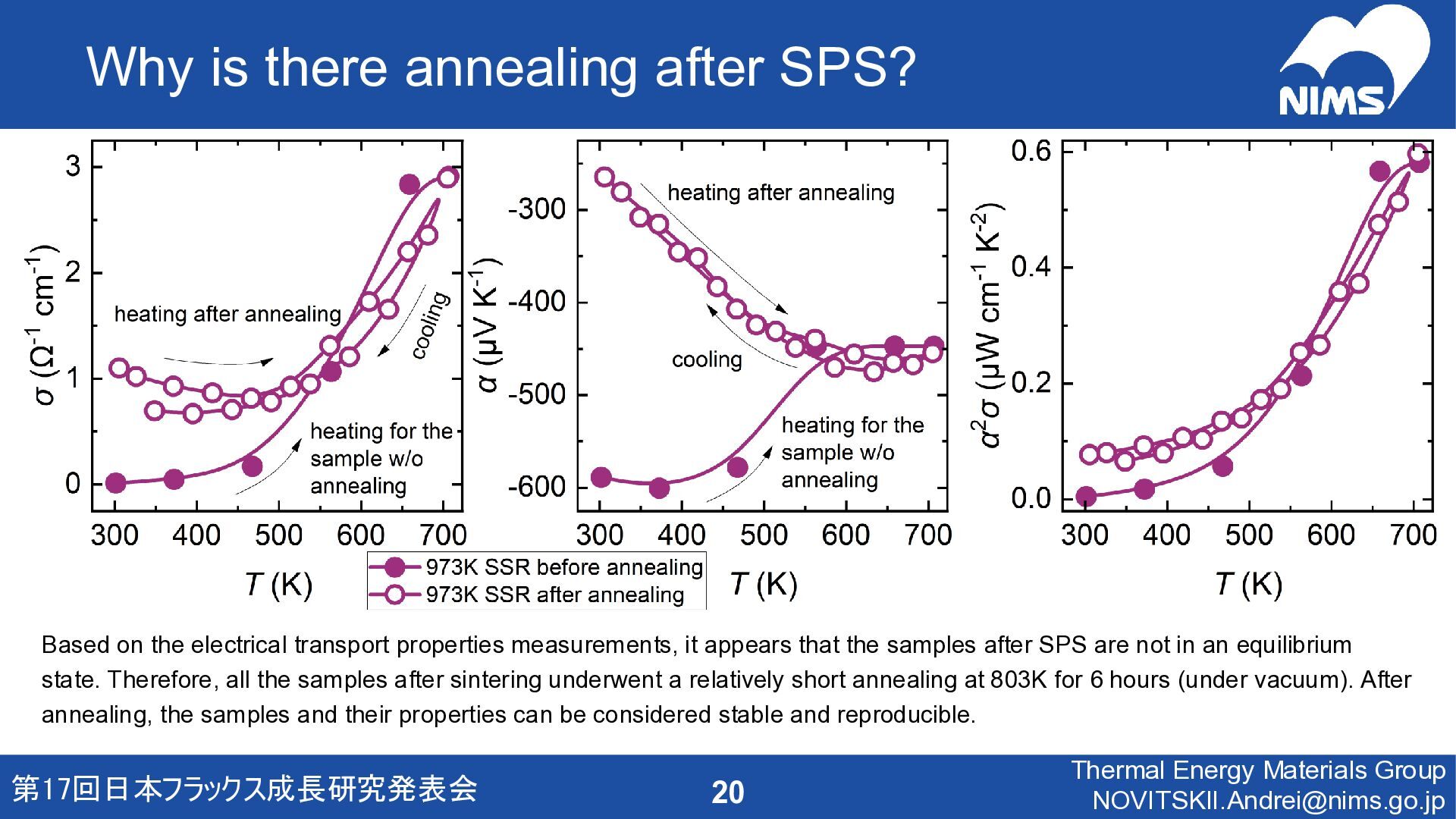
electrical transport properties measurements, it appears that the samples after SPS are not in an equilibrium state. Therefore, all the samples after sintering underwent a relatively short annealing at 803K for 6 hours (under vacuum). After annealing, the samples and their properties can be considered stable and reproducible. 第17回日本フラックス成長研究発表会 Thermal Energy Materials Group [email protected]
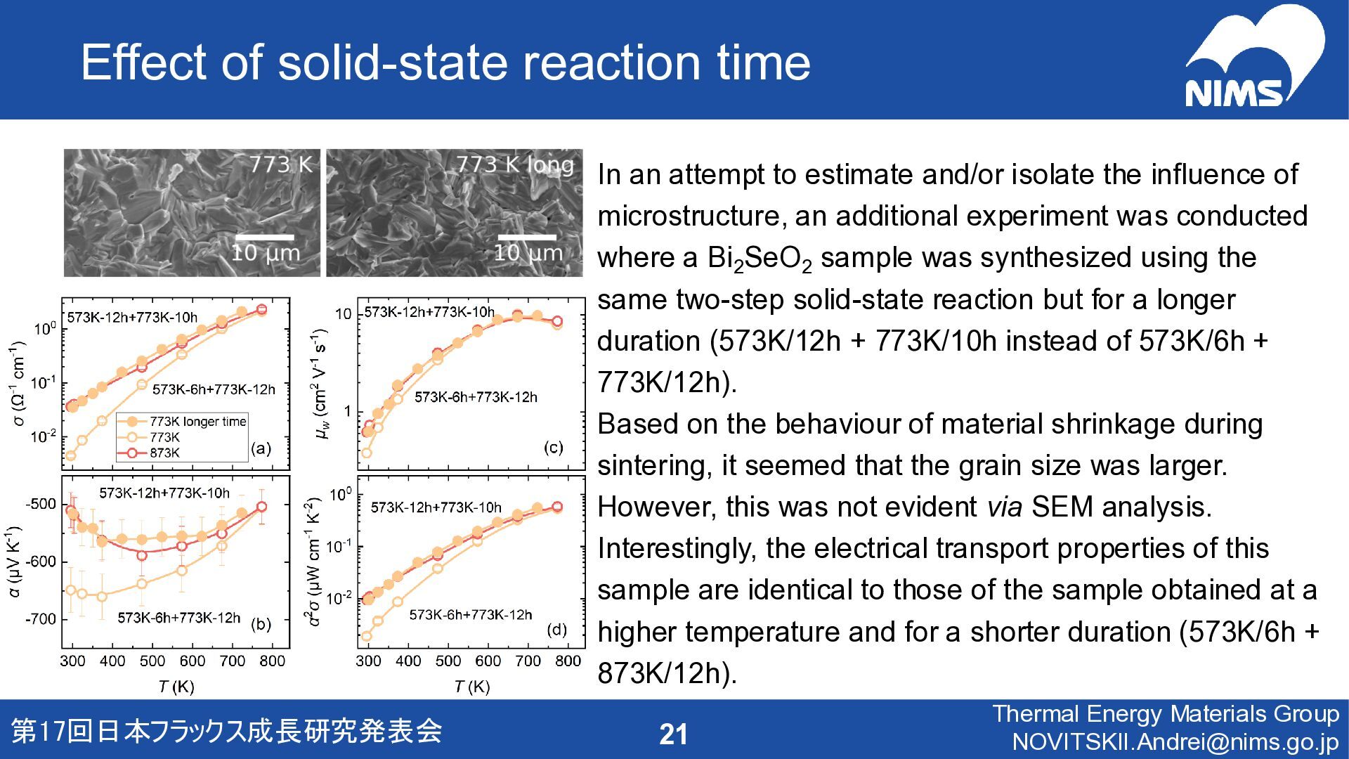
estimate and/or isolate the influence of microstructure, an additional experiment was conducted where a Bi2 SeO2 sample was synthesized using the same two-step solid-state reaction but for a longer duration (573K/12h + 773K/10h instead of 573K/6h + 773K/12h). Based on the behaviour of material shrinkage during sintering, it seemed that the grain size was larger. However, this was not evident via SEM analysis. Interestingly, the electrical transport properties of this sample are identical to those of the sample obtained at a higher temperature and for a shorter duration (573K/6h + 873K/12h). 第17回日本フラックス成長研究発表会 Thermal Energy Materials Group [email protected]
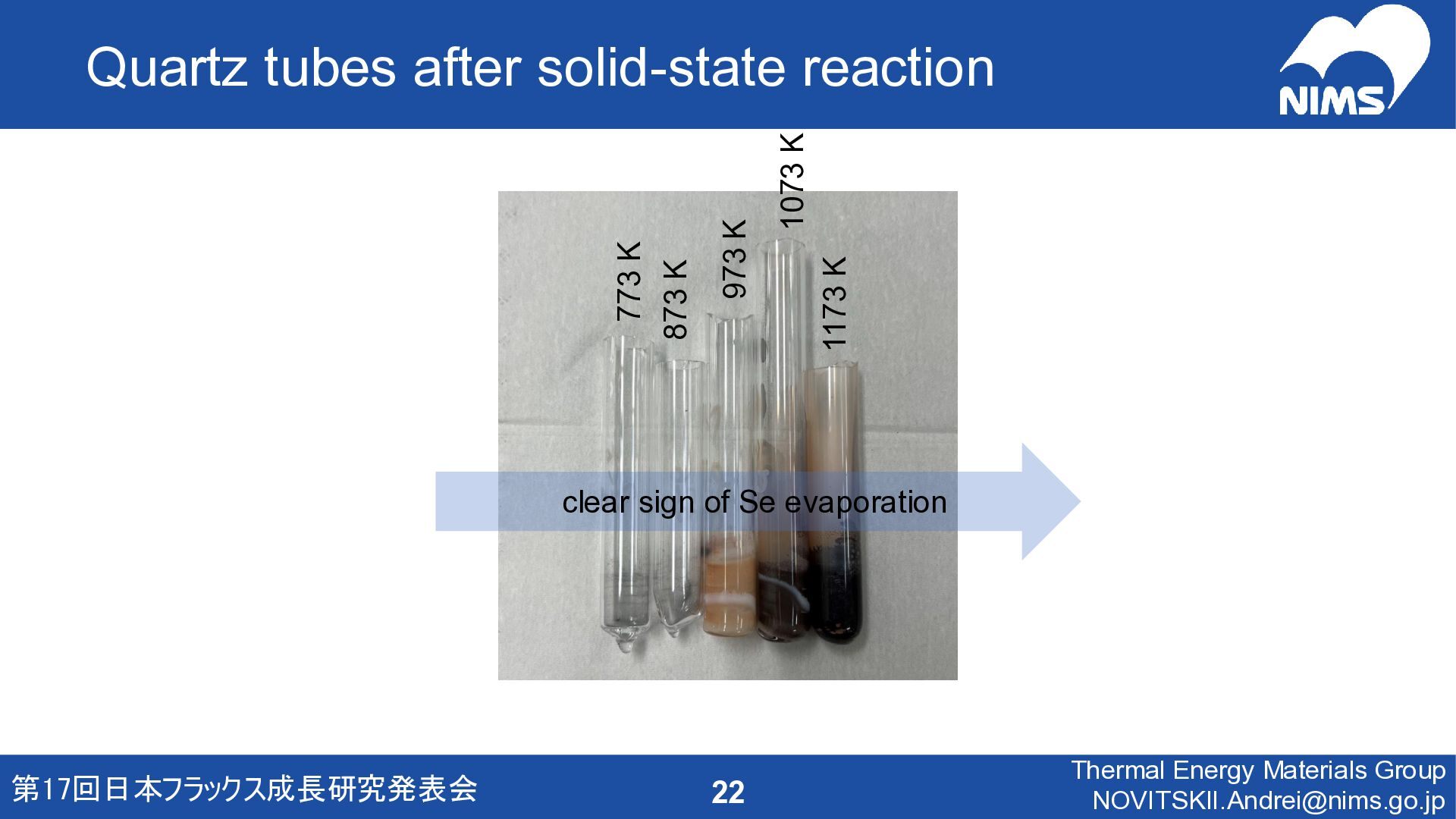
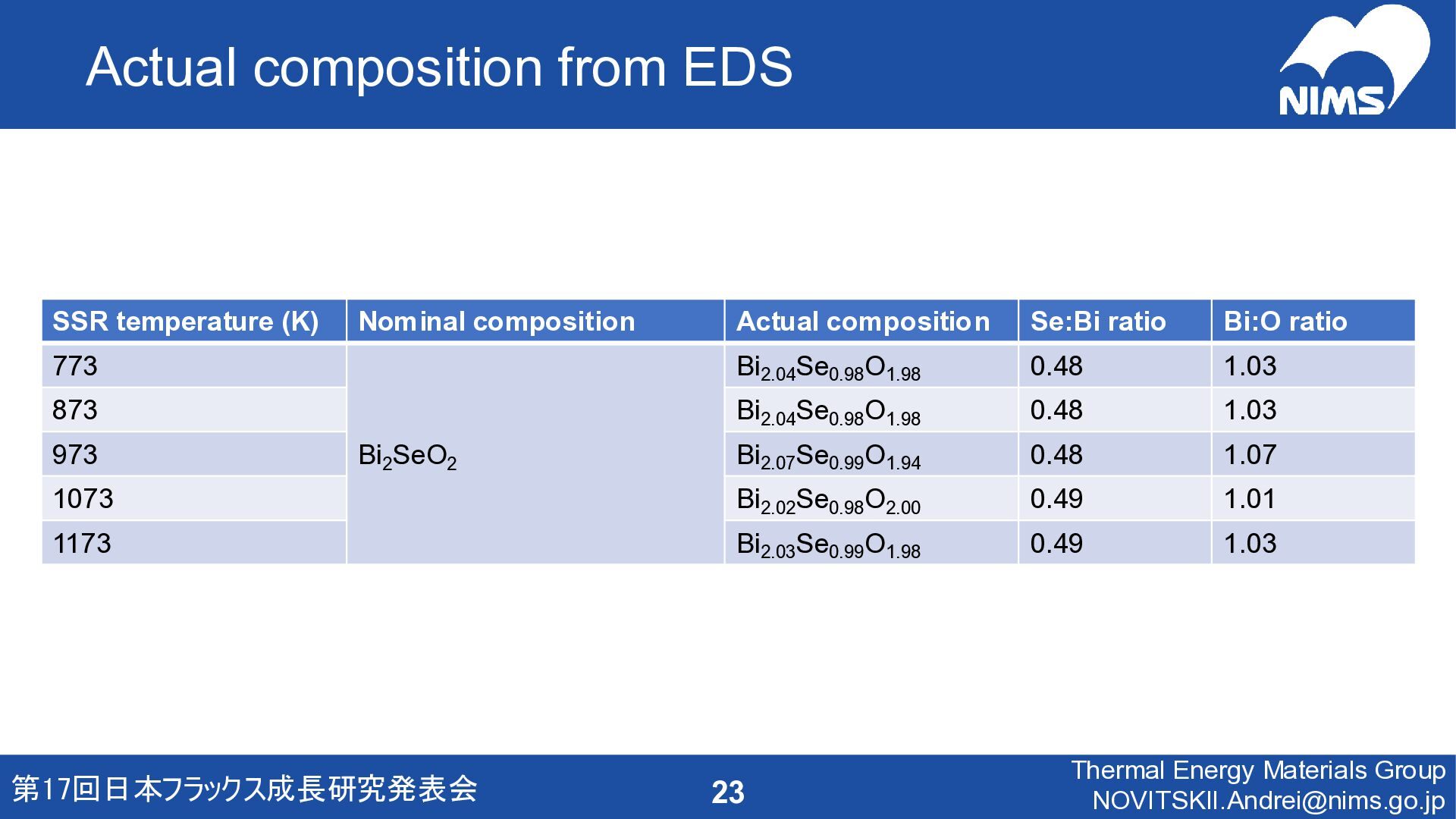
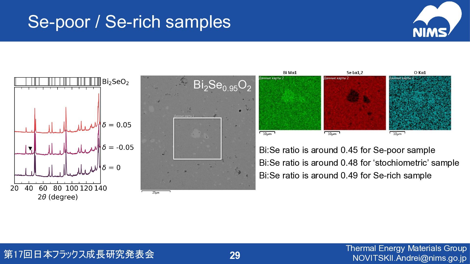
is around 0.45 for Se-poor sample Bi:Se ratio is around 0.48 for ‘stochiometric’ sample Bi:Se ratio is around 0.49 for Se-rich sample 第17回日本フラックス成長研究発表会 Thermal Energy Materials Group [email protected]
![Thermoelectric properties 8 第17回日本フラックス成長研究発表会 Thermal Energy Materials Group [email protected] The](https://files.speakerdeck.com/presentations/249c6d29878e4597aebb6b72b690f26a/slide_7.jpg)
![Conclusions 9 第17回日本フラックス成長研究発表会 Thermal Energy Materials Group [email protected] We combine](https://files.speakerdeck.com/presentations/249c6d29878e4597aebb6b72b690f26a/slide_8.jpg)
![Supporting information Thermal Energy Materials Group [email protected]](https://files.speakerdeck.com/presentations/249c6d29878e4597aebb6b72b690f26a/slide_11.jpg)
![Thermoelectric properties 15 第17回日本フラックス成長研究発表会 Thermal Energy Materials Group [email protected]](https://files.speakerdeck.com/presentations/249c6d29878e4597aebb6b72b690f26a/slide_14.jpg)
![Pisarenko plot 17 第17回日本フラックス成長研究発表会 Thermal Energy Materials Group [email protected] OS](https://files.speakerdeck.com/presentations/249c6d29878e4597aebb6b72b690f26a/slide_16.jpg)