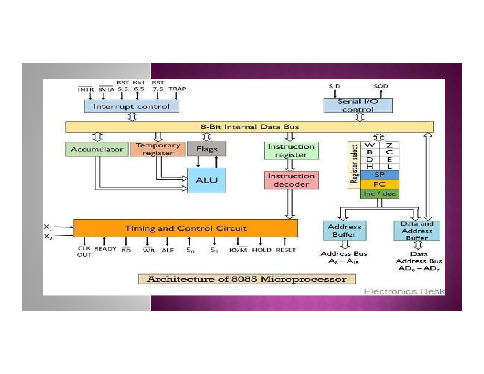
Functional Block Diagram of 8085 Microprocessor, ALU, Accumulator, Registers, Special Function Registers, Data Bus, Address Bus, Interrupts, Flag Register, Temporary Register, etc.
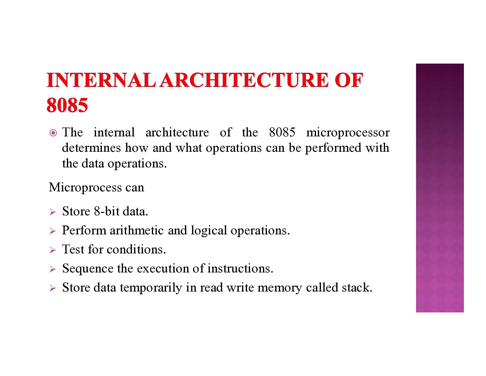
and what operations can be performed with the data operations. Microprocess can Store 8-bit data. Perform arithmetic and logical operations. Test for conditions. Sequence the execution of instructions. Store data temporarily in read write memory called stack.
8-bit data during program execution. These 6 registers are identified as B, C, D, E, H and L. They can be combined as register pairs BC, DE and HL to perform some 16-bit operations. These registers are programmable. It can use to load or transfer data from the registers by using instructions.
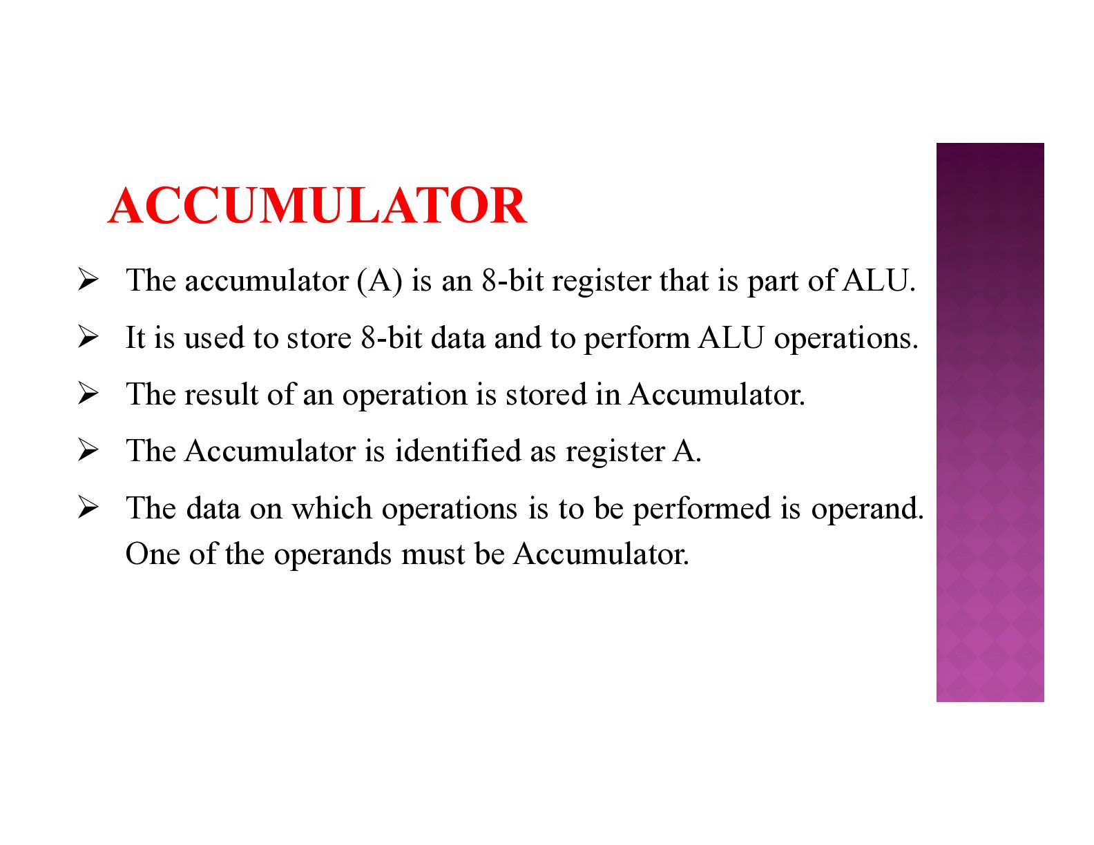
is part of ALU. It is used to store 8-bit data and to perform ALU operations. The result of an operation is stored in Accumulator. The Accumulator is identified as register A. The data on which operations is to be performed is operand. One of the operands must be Accumulator.
the execution of instructions. This register is a memory pointer. Memory locations have 16bit address. The microprocessor uses this register to sequence the execution of the instructions. The function of the program counter is to point to the memory address from which the next byte is to be fetched. When a byte is fetched, the program counter is automatically incremented by one to point the next memory location.
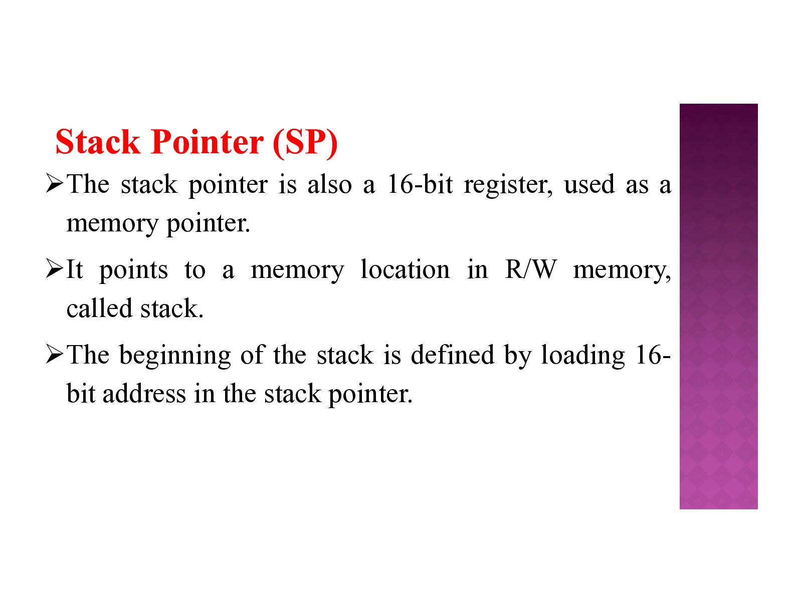
register, used as a memory pointer. It points to a memory location in R/W memory, called stack. The beginning of the stack is defined by loading 16bit address in the stack pointer.
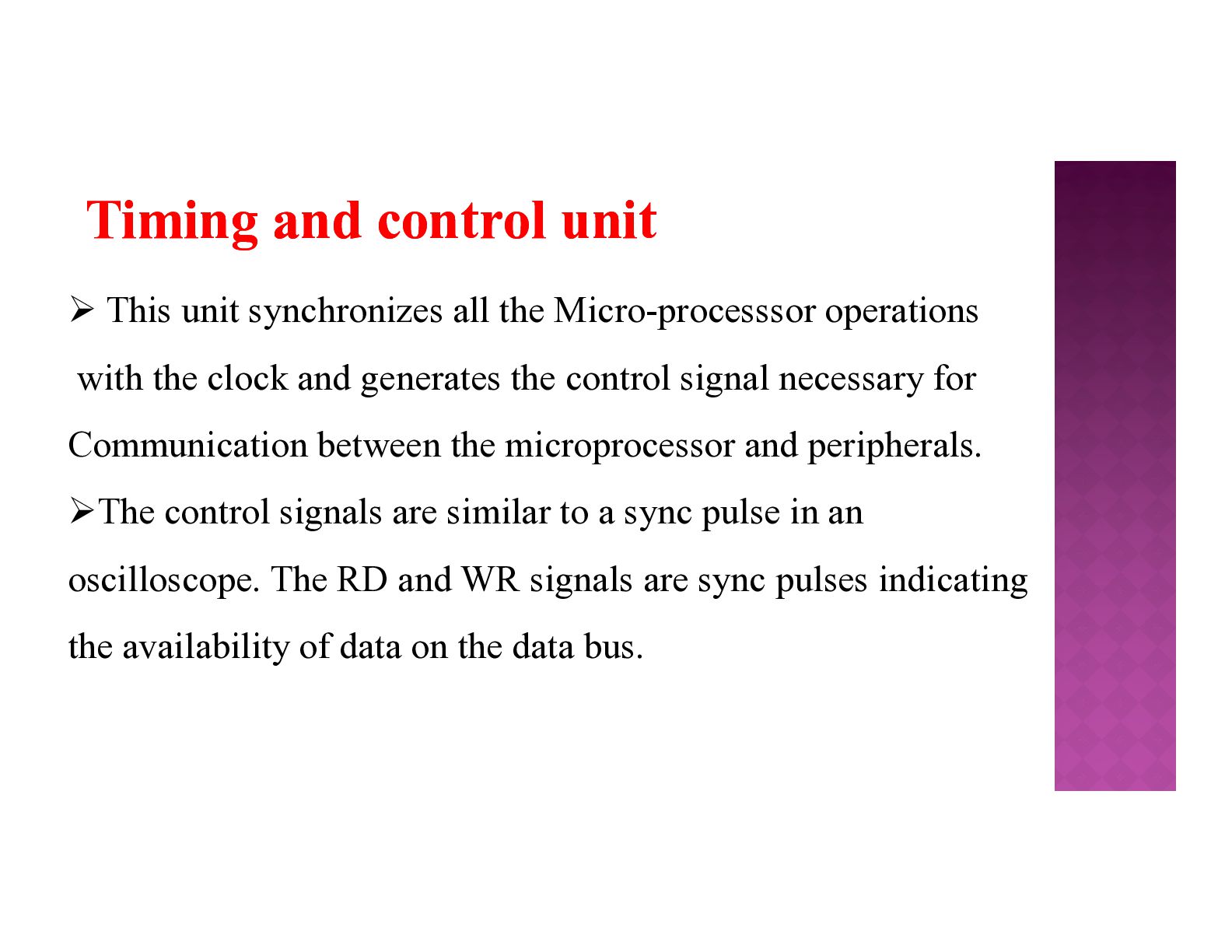
Micro-processsor operations with the clock and generates the control signal necessary for Communication between the microprocessor and peripherals. The control signals are similar to a sync pulse in an oscilloscope. The RD and WR signals are sync pulses indicating the availability of data on the data bus.
are part of the ALU. When an instruction is fetched from the memory it is loaded in to the instruction register. The decoder decodes the instruction and establishes the sequence of events to follow. The instruction register is not programmable and cannot be accessed by any instruction.
registers W and Z, which are included in the register array along with programmable registers namely B, C, D, E, H, L, SP and PC. These registers are used to hold 8-bit data during the execution of instructions. However, they are used internally by microprocessor, they are available to the program.
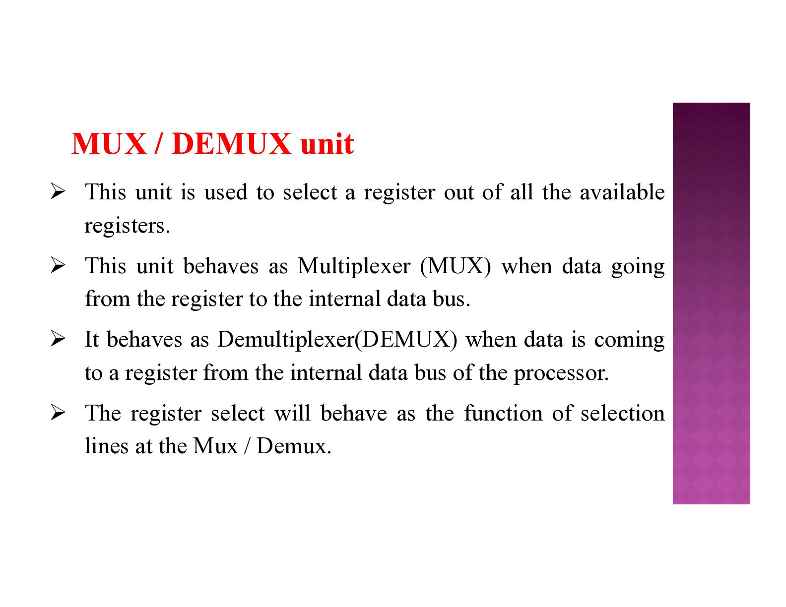
select a register out of all the available registers. This unit behaves as Multiplexer (MUX) when data going from the register to the internal data bus. It behaves as Demultiplexer(DEMUX) when data is coming to a register from the internal data bus of the processor. The register select will behave as the function of selection lines at the Mux / Demux.
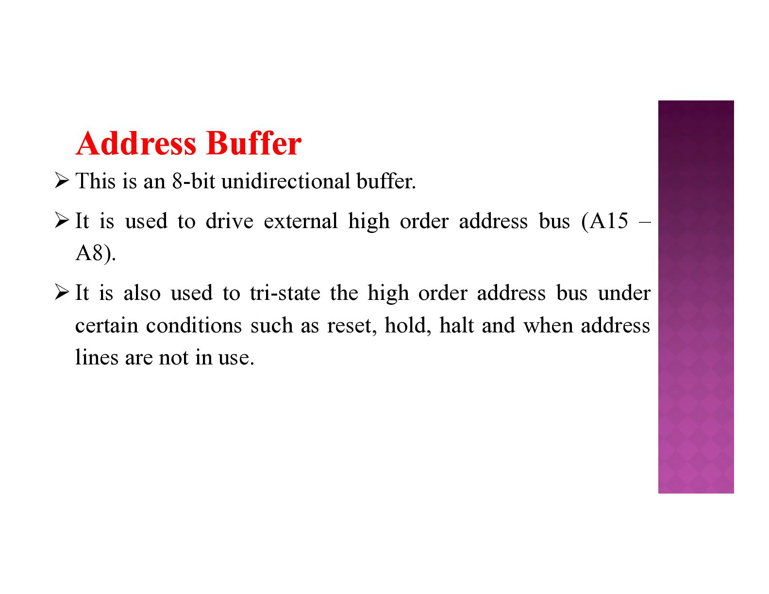
It is used to drive external high order address bus (A15 – A8). It is also used to tri-state the high order address bus under certain conditions such as reset, hold, halt and when address lines are not in use.
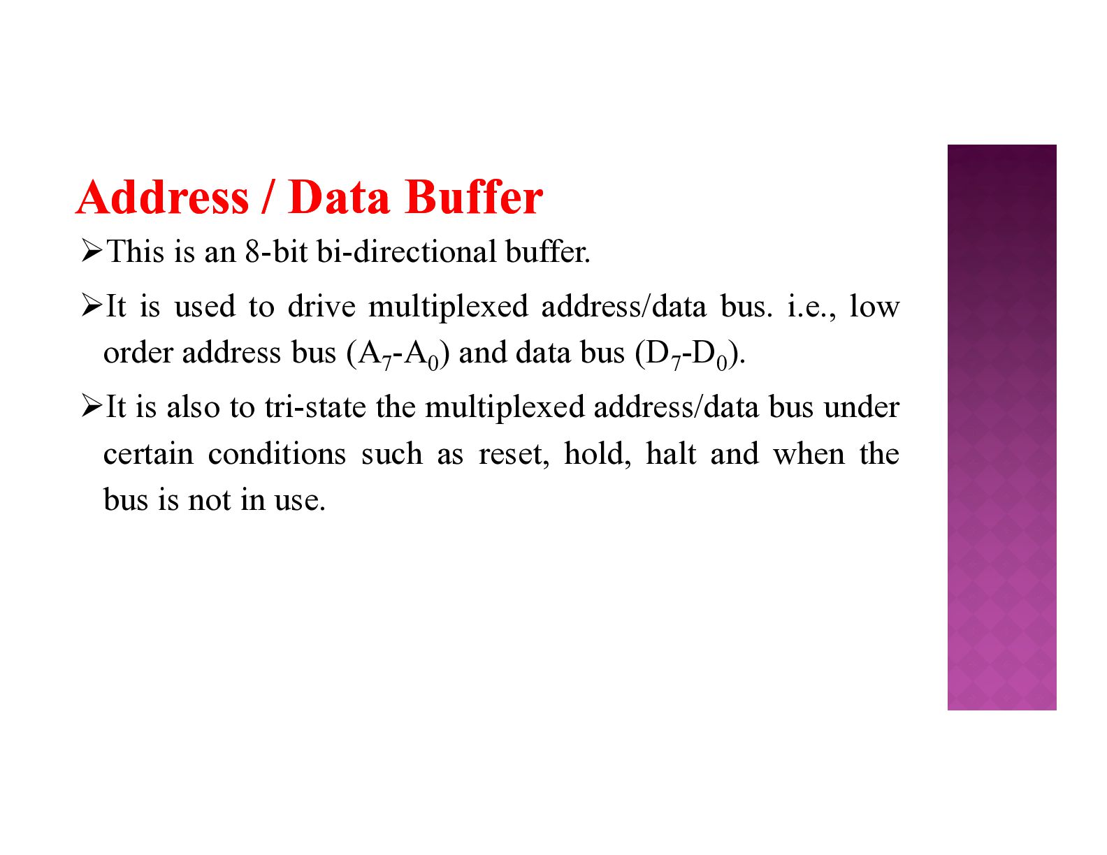
It is used to drive multiplexed address/data bus. i.e., low order address bus (A7-A0) and data bus (D7-D0). It is also to tri-state the multiplexed address/data bus under certain conditions such as reset, hold, halt and when the bus is not in use.
set (or) reset after an operation according to data condition of the result in the accumulator and other registers. They are called Zero (Z), Carry (CY), Sign (S), Parity (P) and Auxiliary Carry (AC) flags. Their bit positions in the flag register are shown in Fig. The microprocessor uses these flags to test data conditions.


 ainischool
 yoshimura_datam
 frievea
 pawan_pharm
 moriyuya
 signer
 sciencetokyo
 hiola
 kaityo256
 mutomasa
 drpoonamkc
 palkan
 stephenakadiri
 bethany
 aleyda
 ryanjones
 csswizardry
 davidcarrasco
 gurzu
 tammyeverts
 soudai
 tmiket