Upgrade to Pro — share decks privately, control downloads, hide ads and more …

FPGAs and Open-Source Hardware - An Intro (Meeting C++ 2016)

FPGAs and Open-Source Hardware - An Intro (Meeting C++ 2016)

FPGAs and Open-Source Hardware - An Intro
Meeting C++ 2016
Lightning Talk

Resources:
https://github.com/MattPD/cpplinks/blob/master/comparch.fpga.md

Matt P. Dziubinski

November 19, 2016
Tweet

More Decks by Matt P. Dziubinski

Other Decks in Programming

Transcript

  1. FPGAs and Open-Source Hardware - An Intro
    Lightning Talk
    Matt P. Dziubinski
    Meeting C++ 2016
    [email protected] // @matt_dz
    Department of Mathematical Sciences, Aalborg University
    CREATES (Center for Research in Econometric Analysis of Time Series)
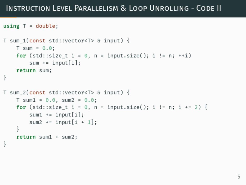
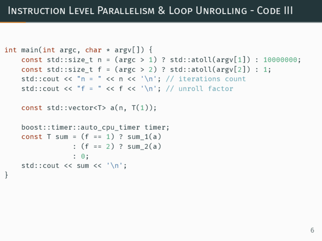
    View Slide

  2. FPGAs
    2

    View Slide

  3. 40 Years of Microprocessor Trend Data
    https://www.karlrupp.net/2015/06/40-years-of-microprocessor-trend-
    data/
    3

    View Slide

  4. Instruction Level Parallelism & Loop Unrolling - Code I
    #include
    #include
    #include
    #include
    #include
    #include
    4

    View Slide

  5. Instruction Level Parallelism & Loop Unrolling - Code II
    using T = double;
    T sum_1(const std::vector & input) {
    T sum = 0.0;
    for (std::size_t i = 0, n = input.size(); i != n; ++i)
    sum += input[i];
    return sum;
    }
    T sum_2(const std::vector & input) {
    T sum1 = 0.0, sum2 = 0.0;
    for (std::size_t i = 0, n = input.size(); i != n; i += 2) {
    sum1 += input[i];
    sum2 += input[i + 1];
    }
    return sum1 + sum2;
    }
    5

    View Slide

  6. Instruction Level Parallelism & Loop Unrolling - Code III
    int main(int argc, char * argv[]) {
    const std::size_t n = (argc > 1) ? std::atoll(argv[1]) : 10000000;
    const std::size_t f = (argc > 2) ? std::atoll(argv[2]) : 1;
    std::cout << "n = " << n << '\n'; // iterations count
    std::cout << "f = " << f << '\n'; // unroll factor
    const std::vector a(n, T(1));
    boost::timer::auto_cpu_timer timer;
    const T sum = (f == 1) ? sum_1(a)
    : (f == 2) ? sum_2(a)
    : 0;
    std::cout << sum << '\n';
    }
    6

    View Slide

  7. Instruction Level Parallelism & Loop Unrolling - Results
    make vector_sums 
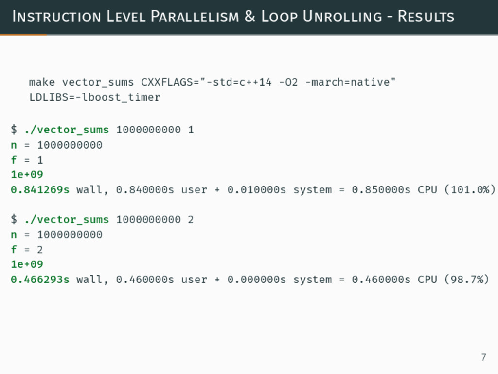
CXXFLAGS="-std=c++14 -O2 -march=native"
    LDLIBS=-lboost_timer
    $ ./vector_sums 1000000000 1
    n = 1000000000
    f = 1
    1e+09
    0.841269s wall, 0.840000s user + 0.010000s system = 0.850000s CPU (101.0%)
    $ ./vector_sums 1000000000 2
    n = 1000000000
    f = 2
    1e+09
    0.466293s wall, 0.460000s user + 0.000000s system = 0.460000s CPU (98.7%)
    7

    View Slide

  8. Microarchitecture
    Intel® 64 and IA-32 Architectures Optimization Reference Manual
    https://www-ssl.intel.com/content/www/us/en/architecture-and-
    technology/64-ia-32-architectures-optimization-manual.html 8

    View Slide

  9. IACA Results - sum_1
    $ iaca -64 -arch IVB -graph ./vector_sums_1i
    Intel(R) Architecture Code Analyzer Version - 2.1
    Analyzed File - ./vector_sums_1i
    Binary Format - 64Bit
    Architecture - IVB
    Analysis Type - Throughput
    Throughput Analysis Report
    --------------------------
    Block Throughput: 3.00 Cycles Throughput Bottleneck: InterIteration
    Port Binding In Cycles Per Iteration:
    -------------------------------------------------------------------------
    | Port | 0 - DV | 1 | 2 - D | 3 - D | 4 | 5 |
    -------------------------------------------------------------------------
    | Cycles | 1.0 0.0 | 1.0 | 1.0 1.0 | 1.0 1.0 | 0.0 | 1.0 |
    -------------------------------------------------------------------------
    N - port number or number of cycles resource conflict caused delay, DV - Divider pipe (on port 0)
    D - Data fetch pipe (on ports 2 and 3), CP - on a critical path
    F - Macro Fusion with the previous instruction occurred
    * - instruction micro-ops not bound to a port
    ^ - Micro Fusion happened
    # - ESP Tracking sync uop was issued
    @ - SSE instruction followed an AVX256 instruction, dozens of cycles penalty is expected
    ! - instruction not supported, was not accounted in Analysis
    | Num Of | Ports pressure in cycles | |
    | Uops | 0 - DV | 1 | 2 - D | 3 - D | 4 | 5 | |
    ---------------------------------------------------------------------
    | 1 | | | 1.0 1.0 | | | | | mov rdx, qword ptr [rdi]
    | 2 | | 1.0 | | 1.0 1.0 | | | CP | vaddsd xmm0, xmm0, qword ptr [rdx+rax*8]
    | 1 | 1.0 | | | | | | | add rax, 0x1
    | 1 | | | | | | 1.0 | | cmp rax, rcx
    | 0F | | | | | | | | jnz 0xffffffffffffffe7
    Total Num Of Uops: 5
    9

    View Slide

  10. IACA Results - sum_2
    $ iaca -64 -arch IVB -graph ./vector_sums_2i
    Intel(R) Architecture Code Analyzer Version - 2.1
    Analyzed File - ./vector_sums_2i
    Binary Format - 64Bit
    Architecture - IVB
    Analysis Type - Throughput
    Throughput Analysis Report
    --------------------------
    Block Throughput: 6.00 Cycles Throughput Bottleneck: InterIteration
    Port Binding In Cycles Per Iteration:
    -------------------------------------------------------------------------
    | Port | 0 - DV | 1 | 2 - D | 3 - D | 4 | 5 |
    -------------------------------------------------------------------------
    | Cycles | 1.5 0.0 | 3.0 | 1.5 1.5 | 1.5 1.5 | 0.0 | 1.5 |
    -------------------------------------------------------------------------
    N - port number or number of cycles resource conflict caused delay, DV - Divider pipe (on port 0)
    D - Data fetch pipe (on ports 2 and 3), CP - on a critical path
    F - Macro Fusion with the previous instruction occurred
    * - instruction micro-ops not bound to a port
    ^ - Micro Fusion happened
    # - ESP Tracking sync uop was issued
    @ - SSE instruction followed an AVX256 instruction, dozens of cycles penalty is expected
    ! - instruction not supported, was not accounted in Analysis
    | Num Of | Ports pressure in cycles | |
    | Uops | 0 - DV | 1 | 2 - D | 3 - D | 4 | 5 | |
    ---------------------------------------------------------------------
    | 1 | | | 0.5 0.5 | 0.5 0.5 | | | | mov rcx, qword ptr [rdi]
    | 2 | | 1.0 | 0.5 0.5 | 0.5 0.5 | | | CP | vaddsd xmm0, xmm0, qword ptr [rcx+rax*8]
    | 1 | 1.0 | | | | | | | add rax, 0x2
    | 2 | | 1.0 | 0.5 0.5 | 0.5 0.5 | | | | vaddsd xmm1, xmm1, qword ptr [rcx+rdx*1]
    | 1 | 0.5 | | | | | 0.5 | | add rdx, 0x10
    | 1 | | | | | | 1.0 | | cmp rax, rsi
    | 0F | | | | | | | | jnz 0xffffffffffffffde
    | 1 | | 1.0 | | | | | CP | vaddsd xmm0, xmm0, xmm1
    Total Num Of Uops: 9
    10

    View Slide

  11. CPUs: General Purpose, Fixed Functionality Hardware
    Intel® 64 and IA-32 Architectures Optimization Reference Manual
    https://www-ssl.intel.com/content/www/us/en/architecture-and-
    technology/64-ia-32-architectures-optimization-manual.html 11

    View Slide

  12. CPUs: General Purpose, Fixed Functionality Hardware
    General purpose flexibility – not
    always needed at all costs.
    What if we need custom pipelines
    with more/custom functional
    units?
    12

    View Slide

  13. FPGAs: Custom Purpose, Reconfigurable Hardware
    We'll make our own functional
    units!
    With look-up-tables and
    flip-flops!
    13

    View Slide

  14. The world’s first FPGA: Xilinx XC2064
    P. Alfke, I. Bolsens, B. Carter, M. Santarini, and S. Trimberger, “It’s an
    FPGA!,” IEEE Solid-State Circuits Mag., vol. 3, no. 4, 2011, pp. 15-20.
    14

    View Slide

  15. Reconfigurable Computing - Trends
    Lesley Shannon, Veronica Cojocaru, Cong Nguyen 
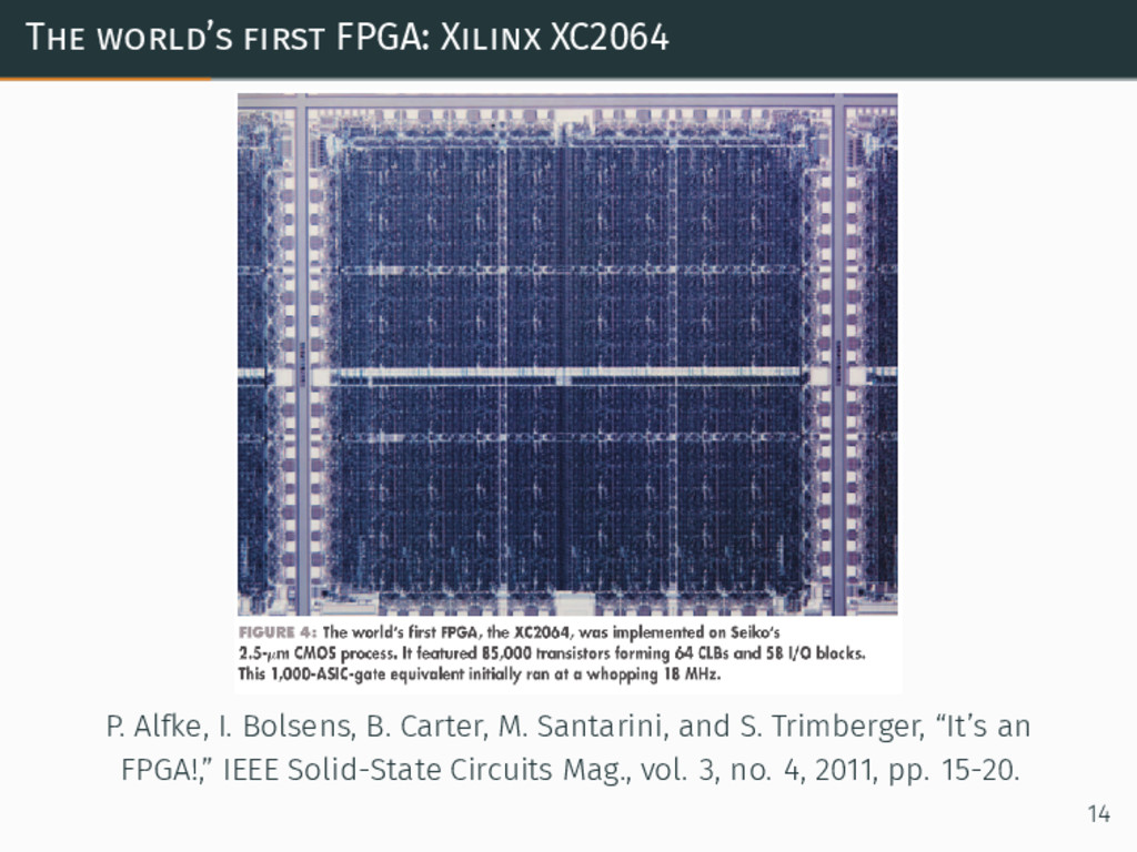
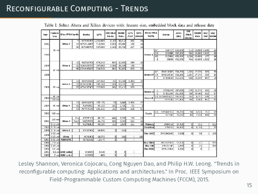
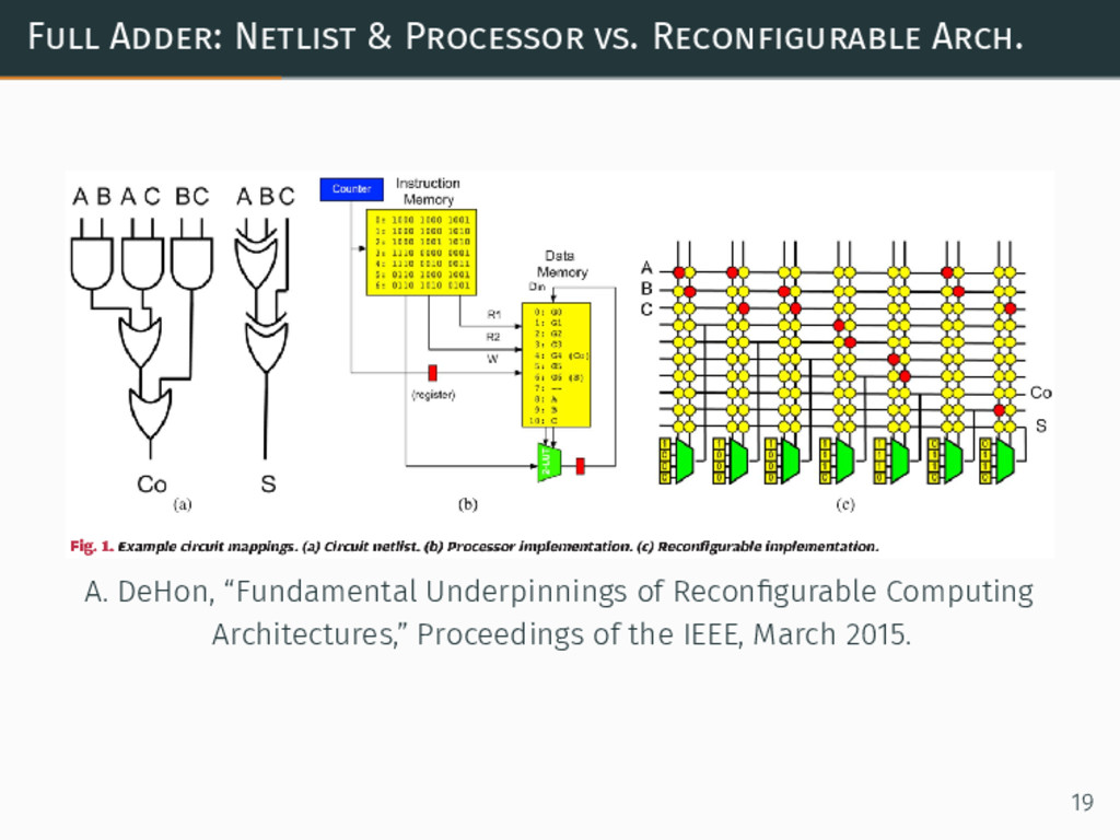
Dao, and Philip H.W. Leong. "Trends in
    reconfigurable computing: Applications and architectures." In Proc. IEEE Symposium on
    Field-Programmable Custom Computing Machines (FCCM), 2015.
    15

    View Slide

  16. Reconfigurable Computing - Progression
    Ahmed, et al., “A 16-nm Multiprocessing
    System-on-Chip Field-Programmable Gate Array
    Platform,” IEEE Micro, Mar-Apr 2016. 16

    View Slide

  17. Reconfigurable Computing - Timeline
    Russell Tessier, Kenneth Pocek, and André DeHon. "Reconfigurable
    Computing Architectures." In Proc. of the IEEE (Special Issue on
    Reconfigurable Systems), Volume 103, Number 3, 2015.
    17

    View Slide

  18. Hardware Description Language (HDL)
    • Hardware description language != software 
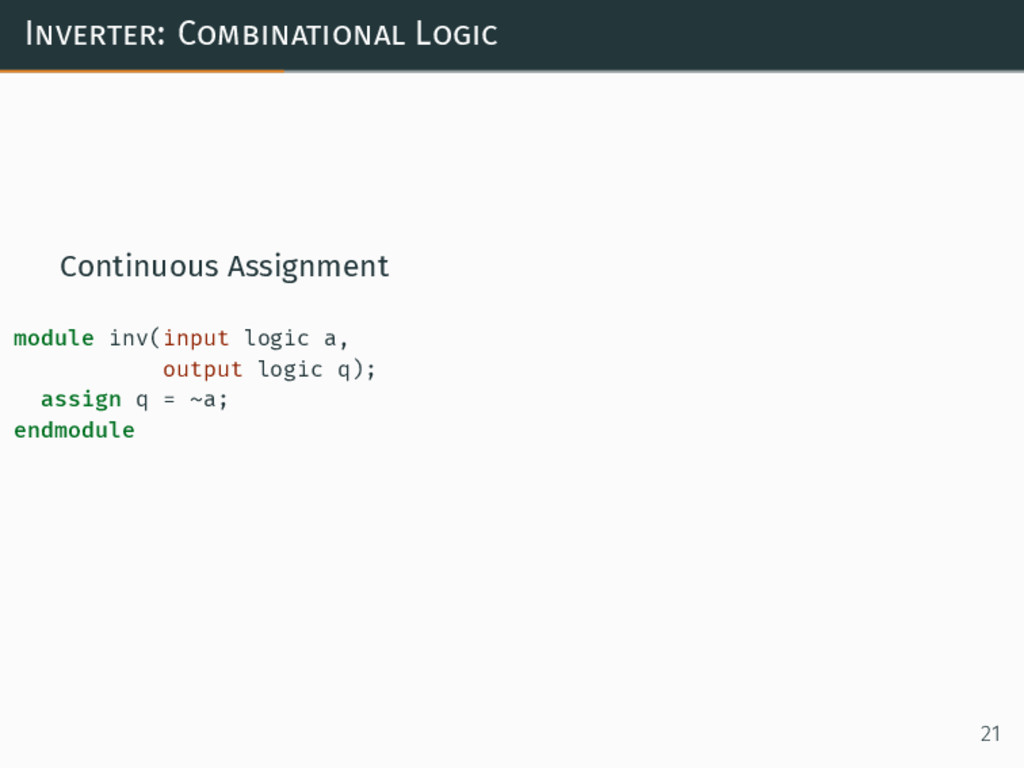
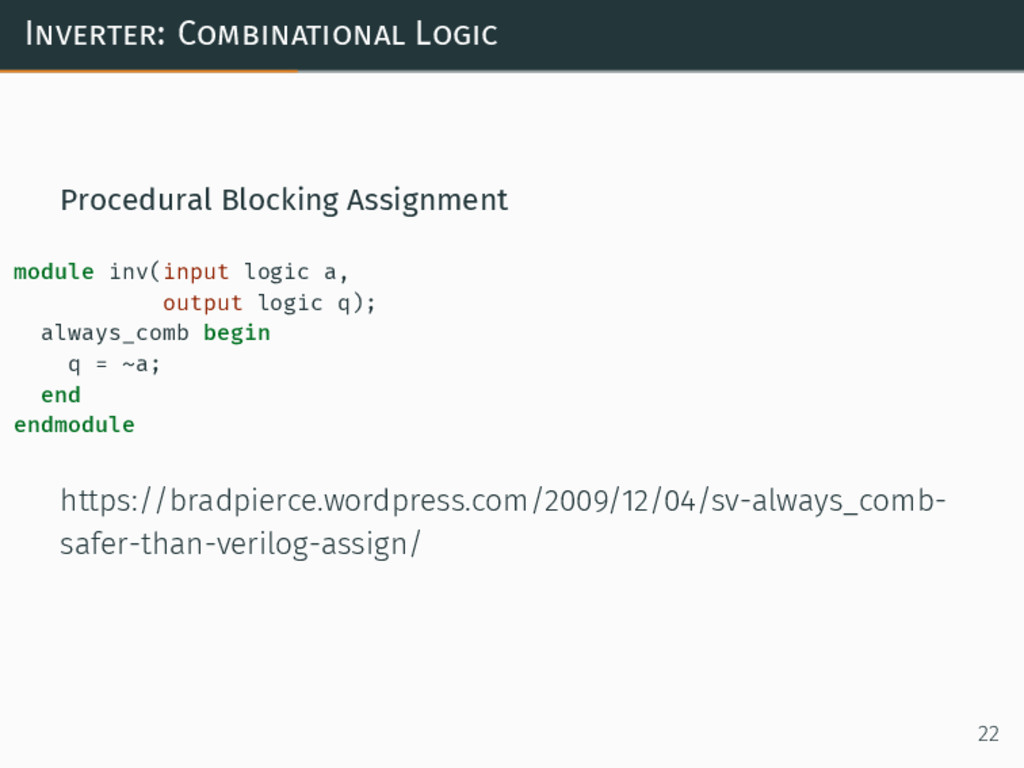
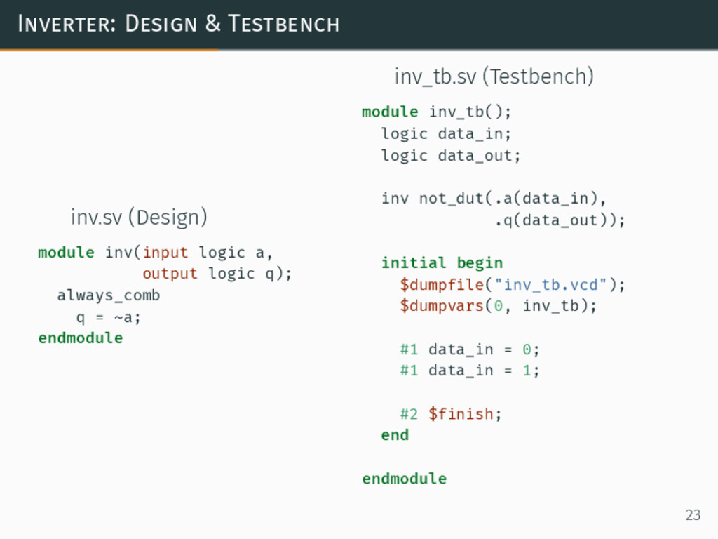
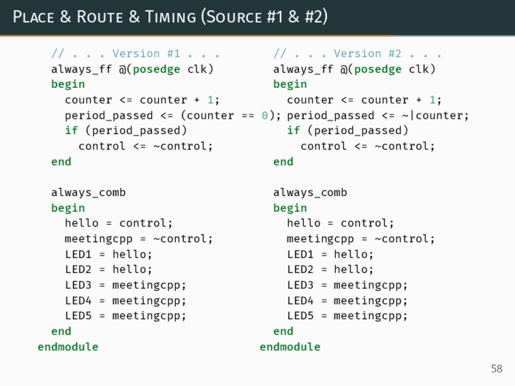
programming
    language
    • Hardware description: Quite different from software
    programming
    • Think: digital circuits design, design entry method happens to be
    using a text format rather than a schematic done with a CAD tool
    • Synthesizable constructs (design) vs. non-synthesizable constructs
    / testbenches (verification)
    • Gotchas: http://www.sutherland-hdl.com/papers.html
    • Verilog (IEEE 1364), SystemVerilog (IEEE 1800), VHDL (IEEE 1076)
    • Toolchain support, degree of standards compliance: extremely
    diverse...
    18

    View Slide

  19. Full Adder: Netlist & Processor vs. Reconfigurable Arch.
    A. DeHon, “Fundamental Underpinnings of Reconfigurable Computing
    Architectures,” Proceedings of the IEEE, March 2015.
    19

    View Slide

  20. SystemVerilog
    • combinational logic
    • outputs - purely a combination of inputs
    • assign continuous assignment statement
    • always_comb procedure
    • blocking assignment statement =
    • sequential logic
    • outputs - also depend on memory (e.g., previous inputs)
    • always_ff procedure
    • nonblocking assignment statement <=
    20

    View Slide

  21. Inverter: Combinational Logic
    Continuous Assignment
    module inv(input logic a,
    output logic q);
    assign q = ~a;
    endmodule
    21

    View Slide

  22. Inverter: Combinational Logic
    Procedural Blocking Assignment
    module inv(input logic a,
    output logic q);
    always_comb begin
    q = ~a;
    end
    endmodule
    https://bradpierce.wordpress.com/2009/12/04/sv-always_comb-
    safer-than-verilog-assign/
    22

    View Slide

  23. Inverter: Design & Testbench
    inv.sv (Design)
    module inv(input logic a,
    output logic q);
    always_comb
    q = ~a;
    endmodule
    inv_tb.sv (Testbench)
    module inv_tb();
    logic data_in;
    logic data_out;
    inv not_dut(.a(data_in),
    .q(data_out));
    initial begin
    $dumpfile("inv_tb.vcd");
    $dumpvars(0, inv_tb);
    #1 data_in = 0;
    #1 data_in = 1;
    #2 $finish;
    end
    endmodule
    23

    View Slide

  24. Design Flow
    "Open-source Hardware: Opportunities and Challenges" Gagan Gupta, Tony Nowatzki, Vinay Gangadhar and Karthikeyan
    Sankaralingam (pre-print: https://arxiv.org/abs/1606.01980) To Appear in IEEE Computer
    24

    View Slide

  25. The IceStorm flow
    • Fully open source Verilog-to-Bitstream flow for iCE40 FPGAs
    • Yosys: Verilog synthesis suite, formal verification
    • Arachne-pnr: place-and-route tool for iCE40
    • IceStorm: tools & docs for iCE40 bitstream
    • including IcePack/IceUnpack, IceBox (icebox_explain), IceTime, IceProg
    • http://www.clifford.at/icestorm/
    • iCE40 FPGAs
    • Lattice iCEstick (HX1K-TQ144)
    • http://www.latticesemi.com/icestick
    • https://octopart.com/search?q=icestick
    • iCE40-HX8K Breakout Board (HX8K-CT256)
    25

    View Slide

  26. Open source projects
    • GTKWave: waveform viewer
    • http://wiki.gedaproject.org/geda:faq#what_is_the_geda_suite
    26

    View Slide

  27. iCE40 HX1K: Block Diagram
    iCE40 LP/HX Family Data Sheet
    http://www.latticesemi.com/~/media/LatticeSemi/Documents/DataSheets/iCE/
    iCE40LPHXFamilyDataSheet.pdf
    27

    View Slide

  28. iCE40 HX1K: Programmable Logic Block (PLB)
    iCE40 LP/HX Family Data Sheet
    http://www.latticesemi.com/~/media/LatticeSemi/Documents/DataSheets/iCE/
    iCE40LPHXFamilyDataSheet.pdf
    28

    View Slide

  29. Inverter Simulation Waveform (Pre-Synthesis)
    # pre-synthesis simulation
    iverilog -g2012 -o inv_pre inv.sv inv_tb.sv
    ./inv_pre
    cp inv_tb.vcd inv_pre_tb.vcd
    gtkwave inv_pre_tb.vcd
    29

    View Slide

  30. Inverter Simulation Waveform (Post-Synthesis)
    # post-synthesis simulation
    yosys -p 'synth_ice40 -top inv -blif inv.blif' inv.sv
    yosys -o inv_syn.v inv.blif
    iverilog -g2012 -o inv_post -D inv_tb.sv inv_syn.v \
    `yosys-config --datdir/ice40/cells_sim.v`
    ./inv_post
    cp inv_tb.vcd inv_post_tb.vcd
    gtkwave inv_post_tb.vcd
    30

    View Slide

  31. Inverter Logic Diagram (Pre-Synthesis)
    read_verilog -sv inv.sv
    show -format png -prefix ./inv_diagram_pre inv
    31

    View Slide

  32. Inverter Logic Diagram (Post-Synthesis)
    read_verilog inv_syn.v
    show -format png -prefix ./inv_diagram_post inv
    32

    View Slide

  33. Hello Meeting C++ (iCE40-HX1K)
    iCEstick iCE40HX1K TQ144
    module hi(input logic clk,
    output logic LED1,
    output logic LED2,
    output logic LED3,
    output logic LED4,
    output logic LED5);
    logic [22:0] counter = 0;
    logic period_passed;
    logic control = 0;
    logic hello;
    logic meetingcpp;
    always_ff @(posedge clk)
    begin
    counter <= counter + 1;
    period_passed <= (counter == 0);
    if (period_passed)
    control <= !control;
    end
    assign hello = control;
    assign meetingcpp = ~control;
    assign LED1 = hello;
    assign LED2 = hello;
    assign LED3 = meetingcpp;
    assign LED4 = meetingcpp;
    assign LED5 = meetingcpp;
    endmodule
    33

    View Slide

  34. Hello Meeting C++ (iCE40-HX8K)
    iCE40-HX8K Breakout Board iCE40HX8K CT256
    module hi(input logic clk,
    output logic LED1,
    output logic LED2,
    output logic LED3,
    output logic LED4,
    output logic LED5,
    output logic LED6,
    output logic LED7,
    output logic LED8);
    logic [22:0] counter = 0;
    logic period_passed;
    logic control = 0;
    logic hello;
    logic meetingcpp;
    always_ff @(posedge clk)
    begin
    counter <= counter + 1;
    period_passed <= (counter == 0);
    if (period_passed)
    control <= !control;
    end
    assign hello = control;
    assign meetingcpp = ~control;
    assign LED1 = hello;
    assign LED2 = hello;
    assign LED3 = meetingcpp;
    assign LED4 = meetingcpp;
    assign LED5 = hello;
    assign LED6 = meetingcpp;
    assign LED7 = hello;
    assign LED8 = meetingcpp;
    endmodule 34

    View Slide

  35. PCF (Physical Constraints File) (iCE40-HX1K)
    # iCEstick iCE40HX1K TQ144 clk & LED pins
    set_io clk 21
    set_io LED1 99
    set_io LED2 98
    set_io LED3 97
    set_io LED4 96
    set_io LED5 95
    Source: Datasheet / Pinout Diagram (next slide)
    35

    View Slide

  36. iCEstick iCE40HX1K TQ144 Pinout Diagram
    https://github.com/Obijuan/open-fpga-verilog-tutorial/blob/master/tutorial/doc/images/icestick_pinout.png 36

    View Slide

  37. PCF (Physical Constraints File) (iCE40-HX8K)
    # iCE40-HX8K Breakout Board iCE40HX8K CT256 clk & LED pins
    set_io clk J3
    set_io LED1 B5
    set_io LED2 B4
    set_io LED3 A2
    set_io LED4 A1
    set_io LED5 C5
    set_io LED6 C4
    set_io LED7 B3
    set_io LED8 C3
    37

    View Slide

  38. iCEstick iCE40HX1K TQ144 Makefile
    hi.asc: hi.sv hi.pcf
    yosys -q -p "synth_ice40 -blif hi.blif" hi.sv
    arachne-pnr -d 1k -p hi.pcf hi.blif -o hi.asc
    hi.bin: hi.asc
    icebox_explain hi.asc > hi.ex
    icepack hi.asc hi.bin
    timing.txt: hi.asc
    icetime -tmd hx1k hi.asc > timing.txt
    configure: hi.bin
    iceprog hi.bin
    clean:
    rm -f hi.blif hi.asc hi.ex hi.bin
    .PHONY: clean configure
    38

    View Slide

  39. iCE40-HX8K Breakout Board iCE40HX8K CT256 Makefile
    hi.asc: hi.sv hi.pcf
    yosys -q -p "synth_ice40 -blif hi.blif" hi.sv
    arachne-pnr -d 8k -p hi.pcf hi.blif -o hi.asc
    hi.bin: hi.asc
    icebox_explain hi.asc > hi.ex
    icepack hi.asc hi.bin
    timing.txt: hi.asc
    icetime -tmd hx8k hi.asc > timing.txt
    configure: hi.bin
    iceprog hi.bin
    clean:
    rm -f hi.blif hi.asc hi.ex hi.bin
    .PHONY: clean configure
    39

    View Slide

  40. IceTime: Timing Reports
    // Reading input .asc file..
    // Reading 1k chipdb file..
    // Creating timing netlist..
    icetime topological timing analysis report
    ==========================================
    . . .
    Total number of logic levels: 23
    Total path delay: 5.55 ns (180.20 MHz)
    40

    View Slide

  41. Open-Source Hardware
    41

    View Slide

  42. RISC-V
    RISC-V: The Free and Open RISC Instruction Set Architecture
    https://riscv.org/
    https://riscv.org/2016/10/5th-risc-v-workshop-agenda/ 42

    View Slide

  43. PicoRV32 - A Size-Optimized RISC-V CPU
    • PicoRV32 - A Size-Optimized RISC-V CPU
    https://github.com/cliffordwolf/picorv32
    https://github.com/cliffordwolf/picorv32/tree/master/scripts/icestorm
    • Running a RISC-V core on an IcoBoard
    http://pramode.in/2016/10/23/running-riscv-on-an-icoboard/
    43

    View Slide

  44. ZPU Softcore
    Running ZPU Softcore on Lattice iCE40
    https://sigalrm.blogspot.com/2014/04/running-zpu-softcore-on-
    lattice-ice40.html
    44

    View Slide

  45. RISC-V Open Source Projects
    • BOOM: The Berkeley Out-of-Order RISC-V Processor
    • https://github.com/ucb-bar/riscv-boom
    https://twitter.com/boom_cpu
    • https://ccelio.github.io/riscv-boom-doc/
    • lowRISC - creating a fully open-sourced, Linux-capable, RISC-V-based
    SoC: http://www.lowrisc.org/
    • https://twitter.com/lowRISC
    • https://github.com/lowRISC/lowrisc-chip/
    • mriscv: A 32-bit Microcontroller featuring a RISC-V core
    • https://github.com/onchipuis/mriscv
    https://twitter.com/onchipUIS
    • http://www.onchipuis.io/risc-v
    • PULPino - 32-bit RISC-V microcontroller core:
    http://www.pulp-platform.org/
    • https://twitter.com/pulp_platform
    • https://github.com/pulp-platform/pulpino 45

    View Slide

  46. RISC-V Startup
    SiFive - customized silicon based on the free and open RISC-V
    instruction set architecture
    https://www.sifive.com/
    46

    View Slide

  47. Open Source Processors
    Jonathan Balkind, Michael McKeown, Yaosheng Fu, Tri 
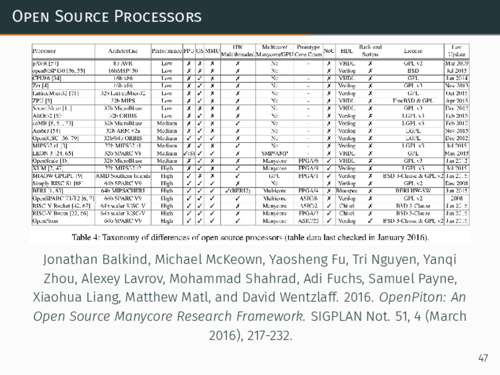
Nguyen, Yanqi
    Zhou, Alexey Lavrov, Mohammad Shahrad, Adi Fuchs, Samuel Payne,
    Xiaohua Liang, Matthew Matl, and David Wentzlaff. 2016. OpenPiton: An
    Open Source Manycore Research Framework. SIGPLAN Not. 51, 4 (March
    2016), 217-232.
    47

    View Slide

  48. Open Source FPGA Projects
    • FPGA Webserver:
    https://github.com/hamsternz/FPGA_Webserver
    • J2 core: a cleanroom reimplementation of the SH-2 ISA with
    extensions: http://j-core.org/
    • "Building a CPU from Scratch: jcore Design Walkthrough":
    http://j-core.org/talks/
    • NetFPGA: http://netfpga.org/
    • https://github.com/NetFPGA/netfpga
    • https://github.com/NetFPGA/NetFPGA-public/wiki
    • Nyuzi Processor: GPGPU processor, SystemVerilog FPGA
    implementation: https://github.com/jbush001/NyuziProcessor
    • TPU: Designing a CPU in VHDL
    • http://labs.domipheus.com/blog/tpu-series-quick-links/
    • Github repository with VHDL sources, ISE project, assembler and
    ISA: https://github.com/Domipheus/TPU 48

    View Slide

  49. FuseSoC
    FuseSoC - package manager and a set of build tools for HDL
    (Hardware Description Language) code for FPGA/ASIC
    development
    https://github.com/olofk/fusesoc
    Olof Kindgren, https://twitter.com/olofkindgren
    49

    View Slide

  50. OpenCores
    OpenCores: Open Source Hardware Community
    http://opencores.org/
    50

    View Slide

  51. FOSSi Foundation & LibreCores
    FOSSi: The Free and Open Source Silicon Foundation
    http://fossi-foundation.org/
    https://twitter.com/FossiFoundation
    LibreCores: Free and Open Source Digital Hardware
    open source hardware community and directory
    https://www.librecores.org/
    https://twitter.com/librecores
    51

    View Slide

  52. Resources
    18-643 Reconfigurable Logic: Technology, Architecture and
    Applications
    http://users.ece.cmu.edu/~jhoe/doku/doku.php?id=18-
    643_reconfigurable_logic
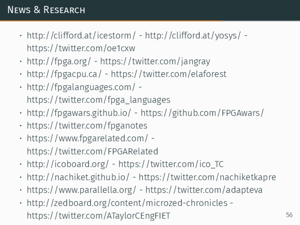
    http://www.clifford.at/icestorm/
    http://www.clifford.at/icestorm/bitdocs-1k/
    http://www.edaplayground.com/
    http://fpgacpu.ca/fpga/
    OH! Open Hardware for Chip Designers
    Silicon proven Verilog library for IC and FPGA designers
    https://github.com/parallella/oh
    https://github.com/parallella/oh#design-guide
    https://github.com/parallella/oh#coding-guide
    52

    View Slide

  53. FPGA History
    P. Alfke, I. Bolsens, B. Carter, M. Santarini, and S. Trimberger, “It’s
    an FPGA!,” IEEE Solid-State Circuits Mag., vol. 3, no. 4, 2011, pp.
    15-20. http://ieeexplore.ieee.org/document/6069771/
    Computer History Museum: Oral History of Bill Carter, designer of
    the first FPGA. Interviewed by Steve Trimberger on 2015-07-13
    https://www.youtube.com/watch?v=1oG-3XWLgog
    "Xilinx and the Birth of the Fabless Semiconductor Industry" by
    Steve Leibson. Chapter of "Fabless: the Transformation of the
    Semiconductor Industry" by Daniel Nenni and Paul McLellan
    https://forums.xilinx.com/xlnx/attachments/xlnx/
    Xcell/200/1/Fabless%20Book%20Chapter%20FINAL.pdf
    53

    View Slide

  54. Verilog
    • EDA Playground Verilog Tutorials - https://www.youtube.com/
    playlist?list=PLScWdLzHpkAfbPhzz1NKHDv2clv1SgsMo
    • HDLBits — Verilog Practice -
    http://verilog.stuffedcow.net/
    • http://hackaday.com/2015/08/19/
    learning-verilog-on-a-25-fpga-part-i/
    • http://hackaday.com/2015/07/28/
    open-source-fpga-toolchain-builds-cpu/
    • https://github.com/Obijuan/
    open-fpga-verilog-tutorial/wiki/Chapter-0%
    3A-you-are-leaving-the-privative-sector
    • Lattice HDL Coding Guidelines - http://www.latticesemi.
    com/~/media/LatticeSemi/Documents/UserManuals/EI/
    HDLcodingguidelines.pdf?document_id=48203
    • Quick Reference for Verilog HDL - https://github.com/
    parallella/oh/blob/master/docs/verilog_reference.md
    54

    View Slide

  55. Conferences & Communities
    ORCONF: An open source digital design conference
    http://orconf.org/
    OSHUG: Open Source Hardware User Group
    http://oshug.org/
    RISC-V Workshops
    https://riscv.org/workshops/
    55

    View Slide

  56. News & Research
    • http://clifford.at/icestorm/ - http://clifford.at/yosys/ -
    https://twitter.com/oe1cxw
    • http://fpga.org/ - https://twitter.com/jangray
    • http://fpgacpu.ca/ - https://twitter.com/elaforest
    • http://fpgalanguages.com/ -
    https://twitter.com/fpga_languages
    • http://fpgawars.github.io/ - https://github.com/FPGAwars/
    • https://twitter.com/fpganotes
    • https://www.fpgarelated.com/ -
    https://twitter.com/FPGARelated
    • http://icoboard.org/ - https://twitter.com/ico_TC
    • http://nachiket.github.io/ - https://twitter.com/nachiketkapre
    • https://www.parallella.org/ - https://twitter.com/adapteva
    • http://zedboard.org/content/microzed-chronicles -
    https://twitter.com/ATaylorCEngFIET 56

    View Slide

  57. Extra Slides
    57

    View Slide

  58. Place & Route & Timing (Source #1 & #2)
    // . . . Version #1 . . .
    always_ff @(posedge clk)
    begin
    counter <= counter + 1;
    period_passed <= (counter == 0);
    if (period_passed)
    control <= ~control;
    end
    always_comb
    begin
    hello = control;
    meetingcpp = ~control;
    LED1 = hello;
    LED2 = hello;
    LED3 = meetingcpp;
    LED4 = meetingcpp;
    LED5 = meetingcpp;
    end
    endmodule
    // . . . Version #2 . . .
    always_ff @(posedge clk)
    begin
    counter <= counter + 1;
    period_passed <= ~|counter;
    if (period_passed)
    control <= ~control;
    end
    always_comb
    begin
    hello = control;
    meetingcpp = ~control;
    LED1 = hello;
    LED2 = hello;
    LED3 = meetingcpp;
    LED4 = meetingcpp;
    LED5 = meetingcpp;
    end
    endmodule
    58

    View Slide

  59. Place & Route & Timing (P&R Version #1)
    place...
    initial wire length = 517
    at iteration #50: temp = 11.1576, wire length = 179
    at iteration #100: temp = 4.43194, wire length = 93
    at iteration #150: temp = 0.917684, wire length = 60
    final wire length = 50
    After placement:
    PIOs 4 / 96
    PLBs 10 / 160
    BRAMs 0 / 16
    place time 0.05s
    route...
    pass 1, 0 shared.
    After routing:
    span_4 13 / 6944
    span_12 4 / 1440
    route time 0.04s
    59

    View Slide

  60. Place & Route & Timing (P&R Version #2)
    place...
    initial wire length = 537
    at iteration #50: temp = 10.5997, wire length = 191
    at iteration #100: temp = 4.21034, wire length = 119
    at iteration #150: temp = 0.917684, wire length = 54
    final wire length = 45
    After placement:
    PIOs 4 / 96
    PLBs 9 / 160
    BRAMs 0 / 16
    place time 0.06s
    route...
    pass 1, 0 shared.
    After routing:
    span_4 13 / 6944
    span_12 1 / 1440
    route time 0.04s
    60

    View Slide

  61. Place & Route & Timing (Timing Report Version #1)
    Report for critical path:
    -------------------------
    lc40_11_7_2 (LogicCell40) [clk] -> lcout: 0.640 ns
    0.640 ns net_21394 (counter[0])
    odrv_11_7_21394_11136 (Odrv12) I -> O: 0.540 ns
    t106 (LocalMux) I -> O: 0.330 ns
    inmux_8_7_17380_17407 (InMux) I -> O: 0.260 ns
    lc40_8_7_0 (LogicCell40) in1 -> carryout: 0.260 ns
    2.029 ns t2
    lc40_8_7_1 (LogicCell40) carryin -> carryout: 0.126 ns
    . . .
    5.549 ns net_15475 (counter[22])
    Resolvable net names on path:
    0.640 ns .. 1.769 ns counter[0]
    2.155 ns .. 2.155 ns $auto$alumacc.cc:470:replace_alu$13.C[2]
    . . .
    5.073 ns .. 5.332 ns $auto$alumacc.cc:470:replace_alu$13.C[22]
    lcout -> counter[22]
    Total number of logic levels: 23
    Total path delay: 5.55 ns (180.20 MHz)
    61

    View Slide

  62. Place & Route & Timing (Timing Report Version #2)
    Report for critical path:
    -------------------------
    lc40_5_8_5 (LogicCell40) [clk] -> lcout: 0.640 ns
    0.640 ns net_9025 (counter[0])
    t42 (LocalMux) I -> O: 0.330 ns
    inmux_6_8_13283_13312 (InMux) I -> O: 0.260 ns
    lc40_6_8_0 (LogicCell40) in1 -> carryout: 0.260 ns
    1.489 ns t2
    lc40_6_8_1 (LogicCell40) carryin -> carryout: 0.126 ns
    . . .
    5.009 ns net_11380 (counter[22])
    Resolvable net names on path:
    0.640 ns .. 1.229 ns counter[0]
    1.615 ns .. 1.615 ns $auto$alumacc.cc:470:replace_alu$14.C[2]
    . . .
    4.532 ns .. 4.792 ns $auto$alumacc.cc:470:replace_alu$14.C[22]
    lcout -> counter[22]
    Total number of logic levels: 23
    Total path delay: 5.01 ns (199.63 MHz)
    62

    View Slide

  63. Select Assign: Else & Priority (#1 & #2)
    // Version #1 (priority)
    module sel_assign(
    input logic s1, s2, d1, d2,
    output logic o1, o2
    );
    always_comb
    begin
    o1 = 1'b0;
    o2 = 1'b0;
    if (s1)
    o1 = d1;
    else if (s2)
    o2 = d2;
    end
    endmodule
    // Version #2 (no priority)
    module sel_assign(
    input logic s1, s2, d1, d2,
    output logic o1, o2
    );
    always_comb
    begin
    o1 = 1'b0;
    o2 = 1'b0;
    if (s1)
    o1 = d1;
    if (s2)
    o2 = d2;
    end
    endmodule
    63

    View Slide

  64. Select Assign: Else & Priority (Logic Diagram #1)
    Note: s1 & inferred priority
    64

    View Slide

  65. Select Assign: Else & Priority (Logic Diagram #2)
    Note: no inferred priority of s1 necessary
    65

    View Slide

  66. Synchronizer (#1 & #2)
    // Version #1 (correct)
    module sync(
    input logic clk,
    input logic d,
    output logic q);
    logic n;
    always_ff @(posedge clk)
    begin
    n <= d;
    q <= n;
    end
    endmodule
    • always_ff &
    nonblocking
    assignment statement
    // Version #2 (incorrect)
    module sync(
    input logic clk,
    input logic d,
    output logic q);
    logic n;
    always_ff @(posedge clk)
    begin
    n = d;
    q = n;
    end
    endmodule
    • issue: always_ff &
    blocking assignment
    statement
    66

    View Slide

  67. Synchronizer (Logic Diagram #1)
    Note: synchronization via intermediate n and 2 flip-flops
    67

    View Slide

  68. "Synchronizer" (Logic Diagram #2)
    Note: useless intermediate n optimized out
    Yosys:
    2.7.3. Executing OPT_CLEAN pass (remove unused cells and wires).
    Finding unused cells or wires in module \sync..
    removing unused `$dff' cell `$procdff$3'.
    removing unused non-port wire \n.
    removed 1 unused temporary wires.
    68

    View Slide

  69. Inverter: Self-Checking Testbench
    module inv_tb();
    logic data_in;
    logic data_out;
    logic data_out_expected;
    logic errors = 0;
    inv not_dut(.a(data_in), .q(data_out));
    initial begin
    $dumpfile("inv_tb.vcd");
    $dumpvars(0, inv_tb);
    data_out_expected = 1;
    data_in = 0; #1;
    $write("data_in: %b, ", data_in);
    $display("data_out: %b", data_out);
    if (data_out !== data_out_expected) begin
    errors = 1;
    $display("Error: input = %b, output = %b (expected: %b)",
    data_in, data_out, data_out_expected);
    end
    data_out_expected = 0;
    data_in = 1; #1;
    $write("data_in: %b, ", data_in);
    $display("data_out: %b", data_out);
    if (data_out !== data_out_expected) begin
    errors = 1;
    $display("Error: input = %b, output = %b (expected: %b)",
    data_in, data_out, data_out_expected);
    end
    $display("Tests: %s", errors ? "FAILED!" : "passed.");
    $finish;
    end
    endmodule
    69

    View Slide

  70. Inverter: Self-Checking Testbench: Output
    iverilog -g2012 -o inv_pre inv.sv inv_tb.sv
    ./inv_pre
    gtkwave inv_tb.vcd &
    VCD info: dumpfile inv_tb.vcd opened for output.
    data_in: 0, data_out: 1
    data_in: 1, data_out: 0
    Tests: passed.
    70

    View Slide

  71. Inverter: Formal Verification with Yosys-SMTBMC
    Reference: http://www.clifford.at/papers/2016/yosys-smtbmc/
    Correct design:
    // inv.sv
    module inv(input logic a, output logic q);
    always_comb
    q = ~a;
    endmodule
    Faulty design:
    // inv.sv
    module inv(input logic a, output logic q);
    always_comb
    q = a; // not an inverter!
    endmodule
    71

    View Slide

  72. Inverter: Formal Verification with Yosys-SMTBMC
    ABV (Assertion Based Verification) & SVA (SystemVerilog
    Assertions)
    // inv_tb.sv
    module inv_tb(input logic data_in);
    logic data_out;
    inv inv_uut(.a(data_in), .q(data_out));
    always_comb begin
    if (!$initstate) begin
    // negation property
    assert(data_out == data_in ^ 1);
    // other examples
    assert(data_out ^ data_in);
    if (!data_in) assert(data_out);
    if (data_out) assert(!data_in);
    assert(data_in != 0 || data_out != 0);
    assert(data_in == 0 || data_out == 0);
    end
    end
    endmodule
    72

    View Slide

  73. Inverter: Formal Verification with Yosys-SMTBMC
    Correct design:
    $ yosys -ql inv.yslog \
    -p 'read_verilog -sv inv.sv' \
    -p 'read_verilog -formal -sv inv_tb.sv' \
    -p 'prep -top inv_tb -nordff' \
    -p 'write_smt2 inv.smt2'
    $ yosys-smtbmc inv.smt2
    ## 0 0:00:00 Solver: z3
    ## 0 0:00:00 Checking asserts in step 0..
    ## 0 0:00:00 Checking asserts in step 1..
    . . .
    ## 0 0:00:00 Checking asserts in step 18..
    ## 0 0:00:00 Checking asserts in step 19..
    ## 0 0:00:00 Status: PASSED
    73

    View Slide

  74. Inverter: Formal Verification with Yosys-SMTBMC
    Faulty design:
    $ yosys -ql inv.yslog \
    -p 'read_verilog -sv inv.sv' \
    -p 'read_verilog -formal -sv inv_tb.sv' \
    -p 'prep -top inv_tb -nordff' \
    -p 'write_smt2 inv.smt2'
    $ yosys-smtbmc inv.smt2
    ## 0 0:00:00 Solver: z3
    ## 0 0:00:00 Checking asserts in step 0..
    ## 0 0:00:00 Checking asserts in step 1..
    ## 0 0:00:00 BMC failed!
    ## 0 0:00:00 Assert failed in inv_tb: inv_tb.sv:15
    ## 0 0:00:00 Assert failed in inv_tb: inv_tb.sv:17
    ## 0 0:00:00 Assert failed in inv_tb: inv_tb.sv:19
    ## 0 0:00:00 Assert failed in inv_tb: inv_tb.sv:12
    ## 0 0:00:00 Status: FAILED (!)
    74

    View Slide

  75. Slides & References
    https://speakerdeck.com/mattpd
    https://github.com/MattPD/cpplinks/blob/master/comparch.fpga.md
    75

    View Slide

  76. Thank You!
    Questions?
    76

    View Slide