INDIA Private Limited, Sonepat Slide: 2 Basic Electronics History: Thermionic emission was observed by Thomas Alva Edison in 1883. In 1904, John Embrose Fleming invented Valve. Lee Dee Forest added another electrode & named it Triode in 1906. Transistor was invented by William Shockley, Bardeen & Brattain in 1947. Jack Kilby invented IC in 1958.
INDIA Private Limited, Sonepat Slide: 4 Basic Electronics Matter: Anything that has mass and occupies space. Matter is found in 3 states. 1. Solids 2. Liquids & 3. Gases.
INDIA Private Limited, Sonepat Slide: 5 Basic Electronics Substance means any solid, liquid or gas. In Solids: 1. Molecules are quite close. 2. It has definite shape & volume.
INDIA Private Limited, Sonepat Slide: 6 Basic Electronics In Liquids: 1. Molecules are relatively at more distances. 2. Definite volume but no definite shape. In Gases: 1. Molecules are at very large distance compared to their size. 2. Neither definite volume nor shape.
INDIA Private Limited, Sonepat Slide: 7 Basic Electronics Matter is composed of small particles called Molecules. Molecules have free existence. A molecule can be further divided into smaller particles called atoms. According to modern theory, the basic constituent of all the matters, whether elements or compounds, is an atom.
INDIA Private Limited, Sonepat Slide: 8 Basic Electronics The electrons may be emitted from an atom by any one of the following methods. 1. Thermionic emission. 2. Field emission. 3. Secondary emission 4. Photo emission & 5. Radio active.
INDIA Private Limited, Sonepat Slide: 9 Basic Electronics What is electronics? The branch of physics that deals with the emission and effects of electrons and with the use of electronic devices. What is emission? The release or discharge of an electron from its parent atom.
INDIA Private Limited, Sonepat Slide: 10 Basic Electronics Structure of an atom? 1. An atom consists of a central part called nucleus. 2. There are protons and neutrons in side the nucleus. 3. In the space around nucleus, electrons revolve in circular or elliptical orbit.
INDIA Private Limited, Sonepat Slide: 12 Basic Electronics Unit positive charged is called protons. 1. It has a charge of 1.6 x 10⁻¹⁹ Coulombs. 2. All protons obtained from different elements are quite identical. 3. Protons rest in the nucleus and they do not move at all. 4. The mass of a proton is 1845 times that of the mass of an electron.
INDIA Private Limited, Sonepat Slide: 13 Basic Electronics Neutrons: 1. It is electrically neutral. 2. Neutrons rest in the nucleus and they also do not move at all. 3. Its mass is almost equal to that of protons. 4. All neutrons obtained from different elements are quite identical.
INDIA Private Limited, Sonepat Slide: 14 Basic Electronics Electrons have two different motions. One is orbital motion due to which they revolve around the nucleus. The second one is spin motion due to which they rotate at their own axis like a top. The same way as earth rotates. Think how day & year changes?
INDIA Private Limited, Sonepat Slide: 15 Basic Electronics Laws governing atomic structure: 1. A normal atom is electrically neutral. Therefore, No. of electrons = No. of protons. It is so because of equal magnitude of charge in an electron and a proton. 2. The number of electrons or protons present in an atom is known as Atomic Number of the element. For example: Cu-29, C-6, Ge-32 etc.
INDIA Private Limited, Sonepat Slide: 16 Basic Electronics 3. The atomic mass or atomic weight of an element is a number, which is equal to the sum of protons and neutrons present in one atom of that element. 4. The distribution of electrons in different orbits is governed by the rule 2n2, where n is the number of orbit. Thus the maximum number of electrons in K, L, M, N, O, P, Q orbits are 2, 8, 18, 18, 8, 2 respectively.
INDIA Private Limited, Sonepat Slide: 17 Basic Electronics 5. For starting a new orbit, its preceding orbit should be completely filled with electrons according to 2n2 law. 6. The last orbit cannot have more than 8 electrons and its preceding orbit cannot have more than 18 electrons. The rule 2n2 is used up to 4 orbits.
INDIA Private Limited, Sonepat Slide: 18 Basic Electronics Ion & Ionisation: 1. An atom remains no longer neutral if it gains or loses one or more electrons. Hence a charged atom is called an ion. 2. An atom having a deficit of electrons is termed as positive ion or cation and an atom having a surplus of electrons is termed as negative ion or anion. 3. The conversion of atoms into ions is known as ionization.
INDIA Private Limited, Sonepat Slide: 19 Basic Electronics How many electrons are there in atom of an element? The relative atomic mass of mercury is 200.59. It means 200.59 gram of mercury shall have 6.023×10²³ atoms. The each atom of mercury has 80 electrons. Therefore,1 gram of Hg shall have 240211376400000000000000 electrons.
INDIA Private Limited, Sonepat Slide: 20 Basic Electronics Inter-Atomic Bonds: The bond between atoms makes it possible to combine to form a solid. Inter-atomic bonds are of three main types: 1. Metallic bond 2. Covalent bond & 3. Ionic bond. These bonds determine the electric conductivity of the materials.
INDIA Private Limited, Sonepat Slide: 21 Basic Electronics Metallic bond: This type of bond exists in metals and their alloys e.g. brass which is the combination of copper & zinc. Stainless steel (composed of iron, chromium, carbon and nickel). 14 karat gold (composed of gold and copper).
INDIA Private Limited, Sonepat Slide: 22 Basic Electronics It is a connection between atoms formed by sharing, rather than transferring electrons. Covalent bond: Si & Ge has 4 electrons in their outer most orbit. They share electrons.
INDIA Private Limited, Sonepat Slide: 23 Basic Electronics Ionic bond: The bond taking place between sodium & chlorine. Sodium (11 electrons) has 1 electron in its outer most orbit and Chlorine (17 electrons) has 7. For some atoms it is easier to lose electrons than to pick up new ones.
INDIA Private Limited, Sonepat Slide: 26 Basic Electronics Conductors are those who have 1, 2 or 3 electrons in their outermost orbit. They are good conductors of heat & electricity. Insulators are those who have 6, 7 or 8. They are bad conductors of both heat & electricity. Semiconductors are those who have 4 electrons & that is why they are neither conductors nor insulators.
INDIA Private Limited, Sonepat Slide: 27 Basic Electronics Intrinsic semiconductors are pure semiconductor without any impurity e.g. silicon & germanium. Extrinsic semiconductors are not pure. They are added with impurity. The process of adding impurity is called doping. Generally 1 to 2 atoms of impurity is added for 1million intrinsic atoms.
INDIA Private Limited, Sonepat Slide: 28 Basic Electronics P-type semiconductor is made when 1 or 2 atoms of Gallium is doped with 1 million atoms of Silicon or Germanium. 3+4=7 electrons means 1 hole is there.
INDIA Private Limited, Sonepat Slide: 29 Basic Electronics N-type semiconductor is made when 1 or 2 atoms of Arsenic is doped with 1 million atoms of Silicon or Germanium. 5+4=9 electrons means 1 extra electron.
INDIA Private Limited, Sonepat Slide: 39 Basic Electronics Ripple Filters: The main function of any ripple filter is to minimise the ripple. Output of various rectifier circuits is pulsating. It has a d.c. component and some a.c. components which are called ripples. This type of output is not useful for driving sophisticated electronic circuits/devices.
INDIA Private Limited, Sonepat Slide: 40 Basic Electronics The ratio between the rms value of ac component of output voltage and the dc components of output voltage is known as ripple factor. For the half-wave rectifier it is 1.21 & for the full wave 0.482. It can be brought to near zero by using ripple filters.
INDIA Private Limited, Sonepat Slide: 43 Basic Electronics 3. It offers high resistance to ac but no resistance to dc components. 4. More effective for heavy load currents. 5. Results in lower dc output. Why? 6. Ripple factor γ , f =50 Hz & L in Henry RL RL γ = ------------------ = --------------------- 3√2.2Πf.L 1330L
INDIA Private Limited, Sonepat Slide: 45 Basic Electronics 3. Discharging time constant should be 100 times than charging time. 4. Capacitor maintains large voltage across the load resistance. 5. Suitable for smaller ripple frequency. 6. Ripple factor γ , f =50 Hz & C in μF. 1 2890 γ = ------------------ = --------------------- 4√3.f.C.RL C.RL
INDIA Private Limited, Sonepat Slide: 46 Basic Electronics LC filter: 1. In inductor filter, ripple factor is directly proportional to load resistance. 2. In capacitor filter, ripple factor it is inversely proportional.
INDIA Private Limited, Sonepat Slide: 47 Basic Electronics 3. When combined, the ripple factor will become independent load resistor. 4. This is called LC filter/inductor input filter/choke input filter etc. 5. Ripple factor γ , f =50 Hz & C in μF & L in Henry. √2 1.195 γ = ------------------ = ------------------ 12.(2Πf)2 LC LC
INDIA Private Limited, Sonepat Slide: 48 Basic Electronics П filter: 1. It is called CLC filter. 2. It is used where low output current and high dc output voltage is required.
INDIA Private Limited, Sonepat Slide: 49 Basic Electronics 3. DC output voltage will be high only when C1 is large (the first capacitor). 4. The ripple factor will be depending upon C1 ×C2 not on C1 + C2 . 5. Ripple factor γ , f =50 Hz & C in μF & L in Henry. 1 5700 γ = --------------------------------- = -------------- 4√2.(2Πf)3.C1 .C2 .L.RL LC
INDIA Private Limited, Sonepat Slide: 51 Basic Electronics We all know that electronic devices needs constant dc voltage for their operation. The dc voltages can be supplied from dry cells or batteries. But these are expensive and needs frequent replacement or charging. Therefore, regulated dc power supply is made by converting the domestic ac supply i.e. 230V50 Hz.
INDIA Private Limited, Sonepat Slide: 52 Basic Electronics The essential element which constitutes a regulated power supply are; 1.Rectifier 2. Filter 3.Voltage regulator.
INDIA Private Limited, Sonepat Slide: 53 Basic Electronics The main reasons of voltage fluctuations in an circuit is; 1. Increase or decrease in input voltage 2. Increase or decrease in load resistor. Therefore, the main task for any voltage regulator is to maintain constant voltage across the load resistor under any of the above 4 conditions.
INDIA Private Limited, Sonepat Slide: 54 Basic Electronics Voltage regulation in % is given by VMAX – VMIN = --------------------------------------- × 100 VMAX Where, VMAX is the maximum dc output voltage VMIN is the minimum dc output voltage.
INDIA Private Limited, Sonepat Slide: 55 Basic Electronics Voltage regulation may also be given in % VNL – VFL = --------------------------------------- × 100 VFL Where, VFL is the full load voltage & VNL is the no load or open circuit voltage of the supply. Smaller the value of voltage regulation better is the power supply!
INDIA Private Limited, Sonepat Slide: 57 Basic Electronics Zener diode shunt regulator: 1. Since Zener is connected in parallel, it is known as shunt regulator
INDIA Private Limited, Sonepat Slide: 58 Basic Electronics 2. A resistance RS is connected in series with the zener to limit the current in the circuit. 3. This is also known as series current limiting resistor. 4. The output VL is taken across the RL . 5. The input voltage must be greater than the VZ .
INDIA Private Limited, Sonepat Slide: 59 Basic Electronics 6. The input current i.e. the current through the limiting resistor is given by VS – VZ divided by RS . 7. VS is the input voltage & VZ is the zener voltage. 8. The ideal zener diode acts as constant voltage source of voltage (VZ ). 9. The practical zener diode has a definite value of resistance called rZ .
INDIA Private Limited, Sonepat Slide: 60 Basic Electronics 10.This causes a voltage drop inside the zener equal to IZ .rZ . 11.Therefore, the voltage across the terminals of zener is equal to load voltage i.e. VL = VZ + IZ .rZ . 12.The current through the load resistor is given by IL = VL /RL . 13.The input current IS = IZ + IL . 14.This also is IZ = IS - IL .
INDIA Private Limited, Sonepat Slide: 61 Basic Electronics Disadvantages: 1. The maximum load current is limited to IZ(MAX) – IZ(MIN) which is of few mA. 2. A large amount of power is wasted in the zener diode and in series resistor. 3. The regulation factor and the output resistance are not very low.
INDIA Private Limited, Sonepat Slide: 62 Basic Electronics Transistor shunt regulator: 1. In this type of voltage regulator, a transistor is connected in parallel with the load that is why the circuit is named.
INDIA Private Limited, Sonepat Slide: 63 Basic Electronics 2. The load voltage VL is equal to the sum of zener voltage VZ & VBE . 3. In other words, VBE = VL – VZ . 4. Since, voltage for a given zener diode is fixed, therefore any increase or decrease in load voltage will have a corresponding effect on the VBE . 5. When VS increases, load voltage also increases.
INDIA Private Limited, Sonepat Slide: 64 Basic Electronics 6. This will cause VBE to increase. 7. Transistor will conduct more. IC will increase forcing VS & IS to increase. 8. IS increases VRS . VL decreases. VS = VRS + VL or VL = VS – VRS . VS ↑→ VL ↑→ VBE ↑→ IC → VRS ↑→ VL↓
INDIA Private Limited, Sonepat Slide: 65 Basic Electronics Transistor series regulator: 1. In this type of voltage regulator, a transistor is connected in series with the load that is why the circuit is named. 2. This is also called emitter follower. 3. The transistor behaves like variable resistance whose value is determined by the base current. 4. VL = VZ – VBE = VZ – VL .
INDIA Private Limited, Sonepat Slide: 66 Basic Electronics 5. When value of load resistance increases, load current decreases, load voltage tends to increase. 6. Increase in load voltage will decrease the base-emitter voltage because zener is fixed. 7. Forward bias to the transistor reduces. 8. Less conduction, increases collector to emitter voltage.
INDIA Private Limited, Sonepat Slide: 67 Basic Electronics 9. This decreases input current to compensate for the increase in the value of load resistor. 10.Thus load voltage may remain at a constant value. 11.The output of a transistor series regulator is approximately equal to the zener voltage VZ . 12.This can be used for larger load.
INDIA Private Limited, Sonepat Slide: 69 Basic Electronics 9. This decreases input current to compensate for the increase in the value of load resistor. 10.Thus load voltage may remain at a constant value. 11.The output of a transistor series regulator is approximately equal to the zener voltage VZ . 12.This can be used for larger load.
INDIA Private Limited, Sonepat Slide: 71 Basic Electronics Voltage multiplier is a circuit, which produces a greater dc output voltage than ac input voltage to the rectifiers. Multipliers are required in many circuits applications where it is necessary to have high voltage with low current. The best example is in the CRT for accelerating purposes.
INDIA Private Limited, Sonepat Slide: 72 Basic Electronics Voltage multipliers are generally; 1. Half wave voltage doublers 2. Full wave voltage doublers 3. Voltage triplers 4. Voltage quadrupler etc.
INDIA Private Limited, Sonepat Slide: 74 Basic Electronics Full wave voltage doublers: During + ve half cycle D1 conducts not D2 . During - ve half cycle D2 conducts not D1 .
INDIA Private Limited, Sonepat Slide: 75 Basic Electronics Voltage tripler & quadruplers: The half wave voltage doubler circuit can be extended to obtain any multiple.
INDIA Private Limited, Sonepat Slide: 79 Basic Electronics It consists of two back to back p-n junctions manufactured in a single crystal. These two junctions give rise to 3 regions called emitter, base & collector.
INDIA Private Limited, Sonepat Slide: 80 Basic Electronics When a layer of n-type material sandwiched between two layers of p-type material, it is called p-n-p transistor. When p-type is sandwiched between layers of n-type, it is called n-p-n transistor.
INDIA Private Limited, Sonepat Slide: 81 Basic Electronics The emitter, base & collector are provided with terminals which are labeled as E, B & C. The 2 junctions are emitter-base junction and collector-base junction.
INDIA Private Limited, Sonepat Slide: 82 Basic Electronics The arrow head is always at the emitter. The arrow head indicates the conventional direction of current flow. In p-n-p, it heads from emitter to base means emitter is more positive than base. Whereas in n-p-n, it is from base to emitter means base is more positive than emitter. Transistors are made by growing, alloying or diffusing.
INDIA Private Limited, Sonepat Slide: 83 Basic Electronics Emitter: It forms the left hand section or region. More heavily doped. Its function is to supply either electrons or holes to the base. Physically it is smaller than collector but larger than base.
INDIA Private Limited, Sonepat Slide: 84 Basic Electronics Base: It forms the middle section of the transistor It is very thin say 10-6m as compared to either the emitter or collector. It is very lightly doped.
INDIA Private Limited, Sonepat Slide: 85 Basic Electronics Collector: It forms the right-hand side region. Main function is to collect either electrons or holes from the emitter and passing through the base. Physically it is largest because it has to dissipate much greater power.
INDIA Private Limited, Sonepat Slide: 86 Basic Electronics The best way to understand emitter, base & collector is to compare as; Emitter as water tank in your house, base as a water tap & collector, the water you collect from the water tap. When you want more water; what do you do? open the tap. Like wise, base current!
INDIA Private Limited, Sonepat Slide: 87 Basic Electronics It is essential for the working of transistor to apply correct polarity across its junction. This is called biasing.
INDIA Private Limited, Sonepat Slide: 88 Basic Electronics Emitter-base junction must be forward biased & collector-base junction must be reverse biased. This can be achieved by 3 ways or configurations.
INDIA Private Limited, Sonepat Slide: 89 Basic Electronics For a p-n-p transistor, collector & base are negative w.r.t. emitter. For n-p-n transistor it is positive w.r.t. emitter.
INDIA Private Limited, Sonepat Slide: 90 Basic Electronics Transistor currents: The three primary currents which flow in the properly biased transistor are; 1. Emitter current IE . 2. Base current IB & 3. Collector current IC . It is seen that IE = IB + IC .
INDIA Private Limited, Sonepat Slide: 91 Basic Electronics By normal convention, currents flowing into a transistor are taken as positive. Current flowing out are taken as negative. Hence, IE is +ve and IB & IC are –ve. Applying Kirchhoff’s law, IE + (-IB ) + (-IC ) =0 IE - IB – IC = 0 or IE = IB + IC This statement is true regardless of transistor type & configuration.
INDIA Private Limited, Sonepat Slide: 92 Basic Electronics Summing up: The four basic guidepost about transistor circuits are; 1. Conventional current flows along arrow whereas electrons flow against it. 2. Emitter-base junction is forward biased. 3. Collector-base junction is reverse biased 4. IE = IB + IC .
INDIA Private Limited, Sonepat Slide: 93 Basic Electronics Transistor circuit configuration: Configuration means circuit connection. Basic there are 3 types of circuit connections. They are; 1. Common base 2. Common emitter and 3. Common collector.
INDIA Private Limited, Sonepat Slide: 94 Basic Electronics Common base configuration: In this configuration, the input signal is applied between base & emitter whereas output is taken out from base & collector. The ratio of collector current to the emitter current is known as alpha of a transistor = IC /IE or IC = IE . The value of of a transistor ranges from 0.95 to 0.99 but not equal to 1.
INDIA Private Limited, Sonepat Slide: 95 Basic Electronics Common emitter configuration: In this configuration, the input signal is applied between base & emitter whereas output is taken out from emitter & collector. The ratio of collector current to the base current is known as Beta of a transistor = IC /IB or IC = IB . The value of of a transistor ranges up to 500.
INDIA Private Limited, Sonepat Slide: 96 Basic Electronics Common collector configuration: In this configuration, the input signal is applied between base & collector whereas output is taken out from emitter & collector. The ratio of emitter current to the base current is known as Gamma of a transistor = IE /IB or IE = IB .
INDIA Private Limited, Sonepat Slide: 99 Basic Electronics Transistor has 2 main functions; 1. As a switch & 2. As an amplifier. When transistor is cut off, it means no current flows through it. When it is saturated; maximum current is flowing. Under both the above conditions, it can be made to work as a switch which has either ON or OFF position.
INDIA Private Limited, Sonepat Slide: 100 Basic Electronics The following sub-script is worth remembering. VCC : Supply voltage collector VEE : Supply voltage emitter VBB : Supply voltage base VCE : Voltage between emitter & collector. VCB : Voltage between collector & base. VEB : Voltage between emitter & base.
INDIA Private Limited, Sonepat Slide: 101 Basic Electronics Cut-off point is that point at which transistor doesn’t conduct any current means IB =0, IC =0; hence VCE =VCC . Considering the circuit, VCE =VCC -IC RL At this point, transistor is used as a switch; normally closed.
INDIA Private Limited, Sonepat Slide: 102 Basic Electronics Saturation point is that point at which collector carries maximum current means, IC =βIB ; hence VCE =VCC -IC RL . Considering the circuit, VCE =VCC -IC RL = 0 At this point, transistor is used as a switch; normally open.
INDIA Private Limited, Sonepat Slide: 103 Basic Electronics Importance of VCE : The voltage VCE is very important in checking whether the transistor is; 1. Defective 2. Working in cut-off & 3. In saturation or well into saturation.
INDIA Private Limited, Sonepat Slide: 104 Basic Electronics For amplifier operation, VCE =½VCC that is transistor is operated at approximately ½ ON. In this way, variation in IB in either direction will control IC in both directions. In other words, when IB increases or decreases; IC also increases or decreases.
INDIA Private Limited, Sonepat Slide: 107 Basic Electronics Transistor amplifiers are classified according to their mode of operation. 1. Input 2. Output 3. Frequency response 4. Biasing condition & 5. Transistor configuration.
INDIA Private Limited, Sonepat Slide: 108 Basic Electronics The description may read like this; small signal, class-A, CE configuration, voltage amplifier used in audio circuit means that; 1. The input voltage is small 2. Biasing condition is common emitter 3. Output is voltage amplification. 4. Frequency range is 20 to 20kHz. 5. Class-A means 360° amplification.
INDIA Private Limited, Sonepat Slide: 110 Basic Electronics Characteristics of a CB amplifier: Very low input resistance (30-150Ω) Very high output resistance (500kΩ) Current gain <1 Large voltage gain of about 1500 Power gain up to 30dB. No phase reversal between input & output.
INDIA Private Limited, Sonepat Slide: 112 Basic Electronics Characteristics of a CE amplifier: Moderately low input resistance (1-2kΩ) Output resistance 50kΩ or large. Current gain is between 300-500. Very high voltage gain Produces phase reversal i.e. input and output signals are 180° are out of phase
INDIA Private Limited, Sonepat Slide: 114 Basic Electronics Characteristics of a CE amplifier: High input impedance (20-500kΩ) Low output impedance (500-1kΩ) High current gain i.e. 1+ Voltage gain is less than 1. Power gain of 10-20dB. No phase reversal.
INDIA Private Limited, Sonepat Slide: 115 Basic Electronics Emitter follower: 1. The common collector junction transistor amplifier is commonly called an emitter follower. 2. It is so-called because the output of the circuit appears at the emitter of the transistor and it is approximately equal to the input voltage. That is, the output 'follows' the input.
INDIA Private Limited, Sonepat Slide: 116 Basic Electronics 3. The main parameter for a transistor is called "Beta" or Hfe (also called 'DC current gain'). This is the ratio of the collector current to the base current. 4. For example, if 100μA flows into the base and causes a collector current of 10mA, then the beta (Hfe) is 10/0.1 = 100 which is a good value. 5. Generally, the beta is between 20 and 200.
INDIA Private Limited, Sonepat Slide: 117 Basic Electronics 6. The base voltage is essentially constant at 0.7 to 0.8 volts with respect to the emitter when the transistor is conducting (turned on). 7. If the base voltage is not at least 0.5 volt more positive than the emitter, the transistor will conduct negligible current.
INDIA Private Limited, Sonepat Slide: 118 Basic Electronics 8. In an emitter follower the base will be about 0.75 volts more positive than the emitter. 9. The output of an emitter follower just follows the input, so the voltage gain is essentially one (unity). 10. A big advantage of the emitter follower is it's high input impedance. It doesn't take much power to drive it.
INDIA Private Limited, Sonepat Slide: 121 Basic Electronics Comparison of Amplifiers configurations Characteristics Common Base Common Emitter Common Collector Current gain Near unity () High () Highest (1+) Voltage gain High Very high Near unity Power gain Moderate Highest Lowest Input impedance Lowest Moderate Highest Output impedance Highest Moderate Lowest Phase reversal Input/output No Yes No
INDIA Private Limited, Sonepat Slide: 122 Basic Electronics Amplifier may also be classified on amount of transistor biasing and amplitude of the signal. The main classifications are; Class-A Class-B Class-C Class-AB
INDIA Private Limited, Sonepat Slide: 123 Basic Electronics Class-A Amplifiers: The transistor is so biased that it remains forward biased throughout the input cycle. This results output current to flow for the full cycle of the input signal.
INDIA Private Limited, Sonepat Slide: 124 Basic Electronics Class-B Amplifiers: The transistor is so biased that it remains forward biased only for half input cycle. This results output current to flow for half cycle of the input signal.
INDIA Private Limited, Sonepat Slide: 125 Basic Electronics Class-C Amplifiers: The transistor is so biased that it remains forward biased for less than half input cycle. This results output current to flow for less than half cycle i.e. 120-150° the input signal.
INDIA Private Limited, Sonepat Slide: 126 Basic Electronics Class-AB Amplifiers: The transistor is so biased that it remains forward biased for more than half input cycle. This results output current to flow for more than half cycle i.e. 180° but less than 360° of the input signal. Its characteristics lies somewhere between those of class-A & class-B.
INDIA Private Limited, Sonepat Slide: 127 Basic Electronics Class-B Push-Pull Amplifiers: It employs two identical transistors operating as a single stage of amplification.
INDIA Private Limited, Sonepat Slide: 128 Basic Electronics 2. They are CE in configuration. 3. Transistor A takes positive half cycle whereas B handles negative half cycle. 4. The two outputs are combined. 5. Whenever there is no signal, it doesn’t draw any power from the VCC . 6. Used extensively in audio work like receivers, tape-recorders etc.
INDIA Private Limited, Sonepat Slide: 129 Basic Electronics Advantages: Efficiency is up to 75%. Distortion free output. No saturation of the transformer cores. No power is drawn in the absence of the input signal.
INDIA Private Limited, Sonepat Slide: 130 Basic Electronics Disadvantages: It requires bulky and expensive output transformers. It requires two out of phase input signals which necessitates an input centre tapped transformer. Driver circuit becomes very complicated.
INDIA Private Limited, Sonepat Slide: 131 Basic Electronics Complementary symmetry class-B push- pull amplifier: 1. Complementary amplifier is a pair of closely matched but oppositely doped power transistors.
INDIA Private Limited, Sonepat Slide: 132 Basic Electronics 2. Complementary amplifier is a pair of closely matched but oppositely doped power transistors. 3. One transistor is PNP but another NPN 4. They operate as emitter follower. 5. Input is capacitive coupled whereas output is direct. 6. Transistors do not conduct when input signal is not present.
INDIA Private Limited, Sonepat Slide: 133 Basic Electronics 7. Positive going input signal forces transistor A to conduct and B to cut-off. 8. Push-pull goes on as one is conducting & another goes to cut-off. 9. Unity voltage gain, no phase reversal & high input impedance. 10.Frequency not a limitations since there is no transformer. 11.Less weight.
INDIA Private Limited, Sonepat Slide: 135 Basic Electronics When the output of one amplifier is connected to the input of another amplifier via something; then it is called coupling. The four basic method of couplings are; 1. Resistance-capacitance coupling. 2. Impedance or Inductive coupling 3. Transformer coupling & 4. Direct coupling.
INDIA Private Limited, Sonepat Slide: 136 Basic Electronics R-C coupling: Amplifiers using this type of coupling are known as RC coupled amplifiers. This consists of two single stage transistor amplifiers using CE configuration.
INDIA Private Limited, Sonepat Slide: 137 Basic Electronics The resistors R2 & R3 and capacitor C2 forms the coupling. Capacitor C1 couples the input signal whereas C3 couples out the output signal. The input vi is amplified by transistor Q1 .The dc component is blocked by C2 and signal is further amplified by Q2 . The output signal is twice of the input signal with no phase reversal.
INDIA Private Limited, Sonepat Slide: 138 Basic Electronics Advantages: 1. Expensive or bulky components are not required. Hence, small, light & simple. 2. Overall amplification is higher. 3. Minimum distortions since coils, transformers etc. are not used. 4. Very flat frequency verses gain curve. It gives uniform voltage amplification over wide range.
INDIA Private Limited, Sonepat Slide: 139 Basic Electronics Disadvantages: 1. Not suitable for very low or very high frequency due to capacitive reactance. 2. Large voltage drops across collector load resistors.
INDIA Private Limited, Sonepat Slide: 140 Basic Electronics L-C coupling: Amplifiers using this type of coupling are known as impedance coupled amplifiers. This consists of two single stage transistor amplifiers using CE configuration.
INDIA Private Limited, Sonepat Slide: 141 Basic Electronics Advantages: 1. Hardly any drop across L; hence low collector supply voltage can be used. Disadvantages: 1. Larger, heavier and costlier. 2. Needs protection from magnetic field. 3. Frequency response is not as good as of RC coupling.
INDIA Private Limited, Sonepat Slide: 142 Basic Electronics At low frequencies, the gain is low due to large capacitance offered by the capacitor. Gain remains low even at high frequencies, due to large reactance. LC coupling is therefore suitable only for audio frequencies.
INDIA Private Limited, Sonepat Slide: 143 Basic Electronics Transformer coupling: Amplifiers using this type of coupling are known as transformer coupled amplifiers. This consists of two single stage transistor amplifiers using CE configuration.
INDIA Private Limited, Sonepat Slide: 144 Basic Electronics T1 is the coupling transformer whereas T2 is the output transformer.C1 is the input coupling capacitor whereas C2 , C3 & C4 are the bypass capacitors. Resistors R1 and R2 as well as R4 and R5 form voltage divider circuits whereas R3 and R6 are emitter stabilising resistors. When input signal is coupled through C1 to the base of Q1 , it appears in an amplified form in the primary of T1 .
INDIA Private Limited, Sonepat Slide: 145 Basic Electronics The secondary of T1 applies the signal to the base of Q2 which appears in an amplified form in the primary of T2 . The secondary of T2 finally appears across the matched load R7 . Advantages: 1.More efficient because of low dc resistance in the primary of collector. 2.It provides higher voltage gain.
INDIA Private Limited, Sonepat Slide: 146 Basic Electronics 3. Poor frequency response because transformer is frequency sensitive. 4. Provides impedance matching. Disadvantages: 1. Costly, bulky & expensive. 2. Faces problem at radio frequencies. 3. Poor frequency response 4. Tends to introduce hum.
INDIA Private Limited, Sonepat Slide: 147 Basic Electronics The peak gain occurs due to resonance or tuning effect of inductance and distributed capacitance. Frequency response: At low frequencies, primary reactance is small, the gain is less.
INDIA Private Limited, Sonepat Slide: 148 Basic Electronics Direct coupling: These amplifiers operate without the use of frequency sensitive components like capacitors, inductors and transformers.
INDIA Private Limited, Sonepat Slide: 149 Basic Electronics They are specially suited for amplifying 1. AC signals with frequencies as low as a fraction of a hertz. 2. Change in dc voltages. 3. Any signal current at the base of Q1 is amplified β1 times and appears at the collector of Q1 and becomes base signal for Q2 . Current gain = β1 β2
INDIA Private Limited, Sonepat Slide: 150 Basic Electronics Advantages: 1. Circuit arrangement is very simple & cheap since it uses minimum components. 2. Capable of amplifying signals of low frequency. Disadvantages: 1. It can’t amplify high frequency signals.
INDIA Private Limited, Sonepat Slide: 152 Basic Electronics Darlington pair: It is the name given to a pair of similar transistors, so connected that emitter of one is directly joined to the base of the other as shown below.
INDIA Private Limited, Sonepat Slide: 153 Basic Electronics Darlington pairs are commercially mounted in a single package that has only 3 leads. The main characteristics of Darlington pairs are; 1. Current gain 2. Input impedance and 3. Voltage gain.
INDIA Private Limited, Sonepat Slide: 154 Basic Electronics Advantages: 1. It can be readily formed from two adjacent transistors in an IC. 2. It can transform a low impedance load into a high impedance load. 3. It uses very few components. 4. It provides vary high β values.
INDIA Private Limited, Sonepat Slide: 156 Basic Electronics Load lines and DC bias circuits: The straight line joining cut-off and saturation points of a BJT is called load line. Load line can be drawn when VCC & RL is known.
INDIA Private Limited, Sonepat Slide: 158 Basic Electronics Q-point: The middle point of extreme points (cut- off & saturation) on the load line, is known as Quiescent point or Q-point. The Q-point can be fixed from the data of a transistor given in transistor data books. This reduces the time consuming work of plotting the collector characteristics and the load line.
INDIA Private Limited, Sonepat Slide: 159 Basic Electronics To do so, the following are very important to remember. 1.The chosen VCC must be less than VCE(Max) given in the data book. As far as possible, value of VCC must be restricted to ¾ of VCE(Max) . 2.Fix the Q-point IC at ½ of IC(Max) given in the data book. 3.At the Q-point assume ½ of VCC will be across VCE .
INDIA Private Limited, Sonepat Slide: 160 Basic Electronics 4. From points (2) & (3), find the value of RC . 5. From the HFE value given in data book, fix the approximate value of the base current at the Q-point as given below; 6. Chosen value of IC at the Q-point IB at Q-point = ---------------------------------------------- Typical value of HFE from data book. 7. From the value of IB at the Q-point and allowing a 0.7 volts drop across the base- emitter, calculate the value of RB .
INDIA Private Limited, Sonepat Slide: 162 Basic Electronics Electronic Oscillators: 1. It is a circuit which converts dc energy into ac energy at very high frequency. 2. A source of generating sine, square, saw tooth or pulse shape. 3. Generates ac output without any external applied input. 4. It is an unstable amplifier.
INDIA Private Limited, Sonepat Slide: 164 Basic Electronics Classification: Electronic oscillator may broadly be divided into following two groups. 1. Sinusoidal (harmonic) oscillator 2. Non-sinusoidal (relaxation) oscillator.
INDIA Private Limited, Sonepat Slide: 165 Basic Electronics Sinusoidal oscillator produce an output having sine waveform. This may further be divided in to; 1. Tuned circuits or LC feedback oscillators such as Hartley, Colpitts, Clapp etc. 2. RC phase shift e.g. Wien bridge 3. Negative resistance oscillators such as tunnel diode.
INDIA Private Limited, Sonepat Slide: 166 Basic Electronics 4. Crystal oscillators 5. Heterodyne or beat frequency oscillators. The active devices (BJT’s, FET’s & UJT’s) in the abovementioned circuits may be biased as class-A, AB, B or C. Class-A biasing is used in high quality AF oscillators whereas RF oscillators prefer class-C biasing.
INDIA Private Limited, Sonepat Slide: 167 Basic Electronics Damped oscillations: Oscillations whose amplitude keeps decreasing with time. This is due to the I2R losses taking place continuously.
INDIA Private Limited, Sonepat Slide: 169 Basic Electronics Oscillatory circuit: 1. It is also called LC or tank circuit. 2. This circuit consists of two reactive elements; an inductor & a capacitor. 3. Both are capable of storing energy. 4. Capacitor stores energy in its electric field whenever there is potential difference across its plates.
INDIA Private Limited, Sonepat Slide: 170 Basic Electronics 5. Similarly, an inductor stores energy in its magnetic field whenever current flow through it. 6. Both L & C are suppose to be loss free. 7. Let that the capacitor has been fully charged from a dc source. 8. Since, S is open, it can not discharge through L
INDIA Private Limited, Sonepat Slide: 172 Basic Electronics When switch ‘S’ is closed; 1. Electrons move from plate A to plate B through coil L. 2. Coil L opposes the flow of current but some current does pass. 3. Magnetic field is set up in L which stores the energy. 4. When plate A loses all its electrons, current stops.
INDIA Private Limited, Sonepat Slide: 173 Basic Electronics 5. Magnetic field set in the coil, collapses, emf is induced and according to Lenzs’ law; current flow but in the opposite direction i.e. from plate B to plate A. 6. Now capacitor starts getting charged but in opposite direction till the time potential becomes equal. 7. Once, capacitor is charged fully, it again discharges through L.
INDIA Private Limited, Sonepat Slide: 174 Basic Electronics 8. This sequence of charging and discharging continues. The to and fro motion of electrons between the two plates of capacitor constitutes an oscillatory current. 9. It may be noted that during this process, the electrical energy of the capacitor is converted into magnetic energy of the coil and vice-versa.
INDIA Private Limited, Sonepat Slide: 175 Basic Electronics 10.These oscillations are damped because energy is dissipated and their amplitude becomes zero. 11.There are two reasons for this loss of energy. heat produced in the resistance of the coil and connecting wires. in the form of EM waves that are radiated out due to oscillation.
INDIA Private Limited, Sonepat Slide: 176 Basic Electronics The frequency or the time period of the oscillatory current depends upon; 1. Larger the value of capacitor, greater the charging and discharging time. 2. Larger the self induction, greater the time required for each reversal. 1 159 f = ----------- = --------- kHz 2Π√LC √LC L in μH & C in μF
INDIA Private Limited, Sonepat Slide: 177 Basic Electronics Essential of a feedback LC oscillator: 1. Tank circuit or FDN 2. Amplifier 3. A positive feedback.
INDIA Private Limited, Sonepat Slide: 179 Basic Electronics 5. The parallel tuned LC circuit connected between the base & emitter is FDN. Circuit operation: 1. When ‘S’ is closed, IC increases. 2. L1 & L expands. 3. EB voltage & current increases. 4. Further increase in IC . 5. Increase in feedback.
INDIA Private Limited, Sonepat Slide: 181 Basic Electronics 6. IC goes in to saturation. 7. Meanwhile C gets charged. 8. When no increase in IC , L1 contracts. 9. Less feedback through L. 10.C starts discharging. 11.Decrease in the voltage of C, decreases EB voltage, IC , L1 and finally IC to cut-off.
INDIA Private Limited, Sonepat Slide: 182 Basic Electronics 12. After losing its original charge, capacitor again becomes fully charged though with opposite polarity. 13. Since, transistor is in cut-off state, capacitor discharges through L. 14. EB, IC , L1 & L increases that drives transistor into saturation. 15. This cycle keeps on repeating.
INDIA Private Limited, Sonepat Slide: 183 Basic Electronics Tuned collector oscillator: 1. L1 C1 forms primary winding & combination an oscillatory tank circuit. 2. Positive feedback between CE & EB is provided by transformer secondary winding L2 which is mutually coupled to L1 . 3. AC signal is connected through L2 to emitter via low reactance C2 & C3 .
INDIA Private Limited, Sonepat Slide: 184 Basic Electronics 4. CE configuration gives 180° phase shift and another 180° is given by transformer. 5. R1 & R2 is used for dc biasing. Working: 1. When switch is on, a transient current is developed in the L1 C1 circuit. 2. This initiates natural oscillation.
INDIA Private Limited, Sonepat Slide: 185 Basic Electronics 3. Small emf induced in L2 by mutual inductance causes increase in IB . 4. IB is amplified β times & appears in collector circuit. 5. Part of this amplified energy is used to meet loses. 6. The frequency of oscillatory current is almost equal to resonant frequency.
INDIA Private Limited, Sonepat Slide: 186 Basic Electronics Circuit of tuned collector oscillator Let, Inductance = 100μH fo = 1500kHz What should be the C? C = 133pF!
INDIA Private Limited, Sonepat Slide: 187 Basic Electronics Hartley oscillator: 1. Invented by Ralph Hartley in 1915. 2. Inductively coupled, variable frequency oscillators where the oscillator may be series or shunt fed. 3. Series fed oscillators have poor oscillation stability. 4. Shunt fed are used in radio receivers.
INDIA Private Limited, Sonepat Slide: 189 Basic Electronics 5. Tank circuit has centre tapped inductor and one tuning capacitor. 6. The RF choke at the collector keeps the high frequency ac signal out of VCC . 7. RF choke may be replaced with a resistor in cheaper oscillators. 8. Hartley oscillator coil has three connections i.e. T, P & G. The resistance between T & P < T & G.
INDIA Private Limited, Sonepat Slide: 190 Basic Electronics 9. The oscillator frequency range is in MHz. 10. It can be varied by varying C1 . 11. The frequency may be measured; i. Frequency counter (Direct Read Out) ii. Oscilloscope
INDIA Private Limited, Sonepat Slide: 191 Basic Electronics Advantages: 1. The frequency is simply varied by the net value of C in the tank circuit. 2. The output amplitude remains constant when tuned over the frequency range. 3. The feedback ratio of L1 to L2 remains constant.
INDIA Private Limited, Sonepat Slide: 192 Basic Electronics Disadvantages: 1. The output is rich in harmonic content. 2. Not suitable where a pure sine wave is required.
INDIA Private Limited, Sonepat Slide: 193 Basic Electronics Colpitts oscillator: 1. Invented by Edwin H Colpitts. 2. Key features of this type of oscillator is its simplicity and robustness. 3. It is similar to Hartley oscillator except using split capacitor in tank circuit. 4. Generally used for frequencies > 1MHz.
INDIA Private Limited, Sonepat Slide: 195 Basic Electronics Crystal oscillators: 1. When mechanical stress is applied across the two opposite faces of a crystal, a potential difference is developed across them. It is called Piezo-electric effect. 2. Also, when a potential difference is applied across its two opposite faces, it causes the crystal to expand or contract.
INDIA Private Limited, Sonepat Slide: 196 Basic Electronics 3. If an ac is applied, the crystal is set into vibration. 4. The frequency of vibration is equal to the resonant frequency of the crystal which is determined by its structure. 5. When the frequency of the ac equals the resonant frequency, the amplitude of vibration is maximum. 6. Thinner the crystal higher is vibration.
INDIA Private Limited, Sonepat Slide: 198 Basic Electronics Wien bridge oscillators: 1. Suitable for generating low frequencies in the range of 10Hz to 1MHz. 2. It uses two CE connected RC coupled amplifiers and one RC (Wien) bridge. 3. To avoid more components, they use operational amplifiers. 4. Highly stabilised amplitude, voltage & frequency.
INDIA Private Limited, Sonepat Slide: 200 Basic Electronics Non-Sinusoidal (Relaxation) Oscillators: 1. Those oscillators which generate waveforms other than sine waveform are called non-sinusoidal oscillator. 2. They are also called relaxation oscillator. 3. That include square, rectangular, saw- tooth & pulse shaped.
INDIA Private Limited, Sonepat Slide: 202 Basic Electronics Pulse width 1μs MSR = -------------------- = --------------= 1:4 Time between pulse 4μs PRT (Pulse Repetition Time): Time between beginning of one pulse and that of the other. PRF (Pulse repetition Frequency): It is number of pulses per second.
INDIA Private Limited, Sonepat Slide: 203 Basic Electronics Pulse definition: Time delay td: It is the time interval between the beginning of the input pulse and the time the output voltage reaches 10% of its maximum value. Rise time tr: It is the time taken by the output voltage to rise from 10% to 90% of its maximum value. Turn-on Time TON : = td + tr.
INDIA Private Limited, Sonepat Slide: 205 Basic Electronics Pulse width: It is the time duration of the output pulse measured between two 50% levels of the output pulse. Storage Time ts: Time interval between end of the input pulse and the time when output voltage falls to 90%. Fall Time tf: Time interval during which the output voltage falls from 90% to 10%. Turn-off Time TOFF = ts + tf.
INDIA Private Limited, Sonepat Slide: 206 Basic Electronics Multi-vibrators: 1. These devices are useful as pulse generating, storing & counting circuits. 2. They are two stage amplifiers with positive feedback from the output of one amplifier to the input of second amplifier. 3. The feedback is supplied in such a way that one transistor is driven to
INDIA Private Limited, Sonepat Slide: 207 Basic Electronics saturation and other to cut-off. 4. New set of conditions in which the saturated transistor is driven to cut- off and the cut-off to saturation. 5. Three basic types of multi-vibrators; i. Astable ii. Bistable & iii. Monostable
INDIA Private Limited, Sonepat Slide: 208 Basic Electronics Astable multi-vibrator (AMV): It is also called free running relaxation oscillator. It has no stable state but keeps oscillating between two states of its own without any external excitation. When one is on, the other is off & they continuously switch back & forth at a rate depending on RC time constant.
INDIA Private Limited, Sonepat Slide: 210 Basic Electronics When the power is switched on, one of the transistor will start conducting before the other. Let Q1 starts conducting first. The feedback is such that Q1 will be very rapidly driven to saturation and Q2 to cut-off. Soon, Q1 will come to cut-off and make Q2 to saturation and this goes on.
INDIA Private Limited, Sonepat Slide: 211 Basic Electronics Mono-stable multi-vibrator (MMV): It is also called single shot or one shot. It has one stable state. It can be switched to other state by an external trigger pulse. But it returns to the previous state after a time delay determined by the value of circuit components.
INDIA Private Limited, Sonepat Slide: 213 Basic Electronics The initial stable state is represented by Q2 conducting & Q1 at cut-off. When trigger pulse is applied, this multi- vibrator switches Q2 to cut-off and Q1 to conducting. Soon, it returns to initial stage by the feedback . It remains in this state till another trigger pulse arrives. The pulse duration T = 0.69C1 R1 .
INDIA Private Limited, Sonepat Slide: 214 Basic Electronics Bi-stable Multi-vibrator (BMV): It is called flip-flop multi-vibrator. It has two absolute stable state. It can remain in either of these two states unless an external trigger pulse switches it from one state to the other. It doesn’t oscillates. It has no energy storage element.
INDIA Private Limited, Sonepat Slide: 216 Basic Electronics Whenever, a positive pulse is applied to R, Q2 starts conducting. Collector of Q2 falls to zero & cuts-off Q1 . When positive pulse is applied to S, it brings multi-vibrator to its original state. It is widely used in computer memory circuits, counting circuits & frequency dividing circuit.
INDIA Private Limited, Sonepat Slide: 217 Basic Electronics Schmitt Trigger 1. It is named after its inventor. 2. It closely resembles a multi-vibrator. 3. It has two bi-stable states. 4. It is also called emitter coupled binary oscillator because positive feedback occurs by coupling through emitter resistor RE .
INDIA Private Limited, Sonepat Slide: 219 Basic Electronics Applications: 1. It is frequently used for wave shaping purposes even worn out pulses. 2. It can convert inputs with any wave shape into output pulses having rectangular or square wave shapes. 3. This circuit is often called squarer. 4. It can be used as level detector.
INDIA Private Limited, Sonepat Slide: 221 Basic Electronics Field effect transistor: 1. The FET’s were developed in 1960. 2. Current conduction is done by the flow of one type of carrier i.e. holes or electrons. 3. Current is controlled by the effect of electric field. 4. This has an extremely high input resistance ≈100 M).
INDIA Private Limited, Sonepat Slide: 222 Basic Electronics 5. They are voltage controlled divices. 6. It shows high degree of insulation between input and output. 7. The FET is less noisy than a tube or BJT. 8. More suitable for input stages of low signal amplifier. 9. It is mostly used in high fidelity FM receivers.
INDIA Private Limited, Sonepat Slide: 223 Basic Electronics There are two types of FET; i. JEFT (Junction Field Effect Transistor).& ii. MOSFET (Metal Oxide Semiconductor FET).
INDIA Private Limited, Sonepat Slide: 225 Basic Electronics n-channel: n-channel JFET is constructed using a bar of N-type material into which a pair of P-type are diffused. Three wires are connected to device.
INDIA Private Limited, Sonepat Slide: 226 Basic Electronics One at each end of the channel and the third at the substrate. In a sense, this device is like a pn junction diode except that we have connected two wires to the n-side. Electrons can move along the channel When we apply a voltage between the two end wires, a current will flow along the channel.
INDIA Private Limited, Sonepat Slide: 227 Basic Electronics The flow of electrons from source to drain will depend upon the upon the size and shape of the channel and the properties of the N-type material. When a small –ve voltage through the third wire is given to the substrate, the depletion zones get bigger. Current flow becomes difficult and even stops. This is called pinching off the current.
INDIA Private Limited, Sonepat Slide: 228 Basic Electronics The third current is called gate because it can be used to control the flow of electrons along the channel. If we want to increase the current, a small +ve voltage to the gate needs to be applied which will make depletion zone smaller.
INDIA Private Limited, Sonepat Slide: 229 Basic Electronics If we apply too large +ve gate voltage we will make it possible for channel electrons to cross the walls and move into the substrate. What’s is worse, modern FET’s have such tiny gates that even a small channel-gate will blow up the transistor. A basic rule in practical electronics. Transistors blow up faster than fuses!
INDIA Private Limited, Sonepat Slide: 230 Basic Electronics Comparison between FET & BJT: i. FET is uni-polar device i.e. current in the device is carried either by the electrons or by the holes whereas BJT is bipolar device i.e. current is carried by both electrons and the holes. ii. FET is voltage controlled device whereas BJT is current controlled.
INDIA Private Limited, Sonepat Slide: 231 Basic Electronics iii.FET’s input resistance is of several mega ohms whereas input resistance of BJT is of few kilo ohms. iv. FET has a positive temperature coefficient at high current levels & this characteristic prevents the FET from thermal breakdown. BJT has a negative temperature coefficient at high current level & this characteristic leads the BJT to thermal breakdown.
INDIA Private Limited, Sonepat Slide: 232 Basic Electronics v. FET doesn’t suffer from minority carrier storage effects and therefore has higher switching speeds and cut off frequencies but BJT’s do suffer from minority carriers storage effects and therefore BJT has both lower switching speed and cut off frequencies than that of FET’s. vi.Fabrication of FET’s on IC is simpler than BJT’s.
INDIA Private Limited, Sonepat Slide: 233 Basic Electronics Biasing of JFET: 1. Gates are always reverse biased. Therefore the gate current IG is practically zero. 2. In a n-channel JFET, source channel S is connected to the negative of the DC power supply. And, the positive of the DC power supply is connected to the drain terminal of the JFET.
INDIA Private Limited, Sonepat Slide: 234 Basic Electronics iii.In the p-channel JFET, source is connected to the positive end of the power supply and the drain is connected to the negative end of the power supply unit for the drain to get the holes from the p-channel where the holes are the majority carriers.
INDIA Private Limited, Sonepat Slide: 235 Basic Electronics Applications: 1. As input amplifiers in oscilloscopes, electronic measuring instruments etc. as it doesn’t load much to circuit due to its high impedance. 2. For mixer operations in FM receivers.
INDIA Private Limited, Sonepat Slide: 236 Basic Electronics 3. In logic circuits where it is kept off when there is zero input and is turned on with a very little input power. 4. As voltage variable resistor (VVR) in operational amplifier and tone control circuits. 5. LSI and computer memories because of very small size.
INDIA Private Limited, Sonepat Slide: 237 Basic Electronics Testing of JFET and MOSFET: 1. Measure the resistance by a multimeter between source and drain. Its value should be about 10 k. 2. Multimeter should indicate low resistance between gate and source with one polarity and indicate very high resistance between source and drain when the polarity is changed.
INDIA Private Limited, Sonepat Slide: 238 Basic Electronics 3. When the gate junction is open, it gives high resistance with both the polarities. When junction is shorted, it gives low resistance. 4. While checking MOSFET, the value of resistance between gate and drain should be infinitely high in either polarity. If it gives low resistance, the device is faulty.
INDIA Private Limited, Sonepat Slide: 239 Basic Electronics Step Gate Source Drain Measured Resistance Good FET Bad FET 1 open -ve +ve very low high/very high 2 open +ve -ve very low high/very high 3 -ve open +ve very high low/very low 4 +ve open -ve very low high 5 -ve +ve open low low 6 +ve -ve open low high
INDIA Private Limited, Sonepat Slide: 240 Basic Electronics MOSFET: Is abbreviated for metal oxide semiconductor field effect transistor. It has a source, gate and drain. The gate of the MOSFET is insulated from the channel. Because of this, it is sometimes known as IGFET (Insulated Gate Field Effect Transistor).
INDIA Private Limited, Sonepat Slide: 246 Basic Electronics Integrated Circuits: Is an integrated (put together) form of several components of a circuit on a single chip or wafer of a semiconductor material, generally silicon. IC’s may have hundreds of active and passive components.
INDIA Private Limited, Sonepat Slide: 247 Basic Electronics Active components such as diodes and transistors take much less space on the chip than resistors and capacitors. Transistors are used as resistors instead of fabricating resistors themselves. Components like choke, coils and transformers cannot be fabricated in IC’s because of its physical bulkiness.
INDIA Private Limited, Sonepat Slide: 248 Basic Electronics Therefore, wherever inductors are necessary for a circuit leads are brought out of the IC’s such that inductors can be connected externally to the IC. Most IC’s are designed to be used for more than one application by making small changes in external circuitry. For example, an IC may be used as an amplifier or as an oscillator and so on.
INDIA Private Limited, Sonepat Slide: 249 Basic Electronics Advantages of IC’s: 1. Miniaturization of the electronic gadgets. 2. Drastic decrease in the overall weight. 3. Low power requirement. 4. Increased reliability due to less number of solder connections.
INDIA Private Limited, Sonepat Slide: 250 Basic Electronics 5. Greater flexibility in use of the same IC for circuit configurations. 6. Better functioning under wide range of temperatures. 7. Low cost per IC due to large scale production of IC’s. 8. Easy to replace.
INDIA Private Limited, Sonepat Slide: 251 Basic Electronics Limitations: 1. Large value capacitors and resistors cannot be fabricated. 2. Chokes, inductors and transformers cannot be fabricated. 3. If any one stage inside the IC becomes defective, the complete IC has to be discarded. 4. Handling is very delicate.
INDIA Private Limited, Sonepat Slide: 252 Basic Electronics Operational Amplifiers: 1. Often referred as Op-Amps is a high gain, direct coupled differential amplifier, designed to amplify both DC and AC signals. 2. In early days these amplifiers were used in analogue computers to perform mathematical operations such as addition, multiplication etc. 3. That is why it is called “operational.”
INDIA Private Limited, Sonepat Slide: 253 Basic Electronics 4. It has two inputs and one output. 5. It have a special type of amplifier configuration known as differential amplifier as its first stage.
INDIA Private Limited, Sonepat Slide: 254 Basic Electronics Differential amplifiers stage: 1. A differential amplifier stage consists of two transistors with an input to each transistor. 2. The output is taken between the collectors of the transistors as shown. 3. The most important point to note is, both the transistors have identical characteristics, load resistors, input resistors and a single emitter resistor.
INDIA Private Limited, Sonepat Slide: 255 Basic Electronics 4. Dual power supply (+ve, -ve and GND) is required for differential amplifiers (single supply can also be used with a few extra components).
INDIA Private Limited, Sonepat Slide: 256 Basic Electronics If a dual supply is used & if the amplifier is properly balanced (symmetrical values) the output voltage across the collectors will be equal to the difference of the two input voltages. Hence, this amplifier is called differential amplifier It can be operated in two modes; 1. Common-mode operation 2. Differential-mode operation.
INDIA Private Limited, Sonepat Slide: 257 Basic Electronics Common mode operation: Since both sides of the differential amplifier circuits are identical, if an additional signal of same level and phase is applied to both the inputs, the same output signal results from both collectors. Mathematically; VOUT (COM) = A (V1 – V2 )
INDIA Private Limited, Sonepat Slide: 258 Basic Electronics Where A is the voltage gain of each transistor & V1 & V2 are the base input voltages measured to ground. If both the signals are same in phase & in magnitudes; VOUT = A (V1 – V2 ) = A (V1 – V1 ) = A (0) = 0
INDIA Private Limited, Sonepat Slide: 259 Basic Electronics Where A is the voltage gain of each transistor & V1 & V2 are the base input voltages measured to ground. In practice, since the two halves of the circuit cannot be perfectly identical, instead of zero output there will be a very small output. When inputs are 0.5 V, output in common mode may be 0.025V not zero? Why?
INDIA Private Limited, Sonepat Slide: 260 Basic Electronics Differential mode operation: When two inputs signals are out of phase by 180°, the amplifier amplifies the difference of the input signals. Since, the input signals are of equal in amplitude, but out of phase by 180°, the output signal is equal to twice the gain times the input signal.
INDIA Private Limited, Sonepat Slide: 261 Basic Electronics This can be mathematically written as; VOUT (DIFF) = A [V1 -(-V2 )] If V1 = V2 then VOUT (DIFF) = A (2V1 )
INDIA Private Limited, Sonepat Slide: 262 Basic Electronics Common mode rejection ratio: The advantage of differential amplifiers is, it doesn’t amplify input signals that are in phase. This is known as common- mode signal rejection. CMRR = ADM /ACM . ADM = Amplifier gain in differential mode ACM = Amplifier gain in common mode.
INDIA Private Limited, Sonepat Slide: 263 Basic Electronics Inverting amplifier: The input signal is applied to the inverting ‘+’ (INV) terminal. The non (NON) inverting terminal is grounded. The output is amplified signal of opposite polarity.
INDIA Private Limited, Sonepat Slide: 264 Basic Electronics Non-inverting amplifier: The input signal is applied to the non- inverting ‘-’ (NON) terminal. The inverting (INV) terminal is grounded. The output is amplified signal of in phase polarity.
INDIA Private Limited, Sonepat Slide: 265 Basic Electronics Summing amplifier: Operational amplifier is used as an inverting amplifier to do the summing operation.
INDIA Private Limited, Sonepat Slide: 266 Basic Electronics In the given figure, three input signals are applied to the INV terminal through resistors R1 , R2 & R3 . The amount of negative feedback given to the OP amplifier is dependent on the value of RF divided by each resistor in the feedback path.
INDIA Private Limited, Sonepat Slide: 269 Basic Electronics Timer IC-555: Applications such as square wave, ramp, pulse generators and one shot multi- vibrators etc. require a circuit essentially capable of producing timing intervals. Due to the circuit components count and the delicacy in using transistors, integrated circuits are preferred to transistors.
INDIA Private Limited, Sonepat Slide: 270 Basic Electronics One such most suitable and popular IC for producing time intervals is the 555. This IC is popularly known as 555 timer. Similar to operational amplifier, 555 IC is reliable, easy to use in a variety of applications, and at low cost. The IC 555 can operate from a wide range of supply voltages of + 5 to + 18 volts.
INDIA Private Limited, Sonepat Slide: 271 Basic Electronics IC-555 contains i. Two comparators ii. One transistor iii.Three equal value resistors iv.One flip-flop and v. An output stage.
INDIA Private Limited, Sonepat Slide: 273 Basic Electronics Modes of operation: The timer has two modes of operation; 1.As an astable (free running) & 2.As a mono-stable (one shot).
INDIA Private Limited, Sonepat Slide: 274 Basic Electronics Principle of operation: 1. The threshold input is connected to an external RC timing circuit. 2. If the capacitor charge exceeds the ⅔VCC , reference on the threshold comparator, the comparator is triggered. 3. This sets the flip-flop. 4. Turns on the transistor. 5. Capacitor discharges.
INDIA Private Limited, Sonepat Slide: 275 Basic Electronics Application of astable multi-vibrator: 1. In electronic Pianos: generation of different frequencies with different RC values. 2. Signal injectors: used as testing instrument by service technicians. 3. Flashing lights: advertisements, displays etc.
INDIA Private Limited, Sonepat Slide: 276 Basic Electronics IC-555 timer as VCO: A voltage controlled oscillator (VCO) changes its output frequencies in relation to the input voltage at the control input of the threshold comparator at pin-5.
INDIA Private Limited, Sonepat Slide: 279 Basic Electronics Varactor diode: In a p-n junction diode, a very thin depletion region (an insulator) exists on either side of p-n type semiconductor materials. This forms a capacitor.
INDIA Private Limited, Sonepat Slide: 280 Basic Electronics Since, the width of the depletion region (dielectric) between the two plates of the capacitor can be varied by varying the external voltage applied to the junction, the effective capacitance of the junction also varied accordingly. Therefore, a p-n junction can be used as a voltage variable capacitor (VVC). By changing C, frequency is changed.
INDIA Private Limited, Sonepat Slide: 281 Basic Electronics Applications: 1. Since the junction capacitance of a varactor diode is in the picofarad range, it is suitable for use in high frequency circuits. 2. Automatic frequency control device. 3. FM modulator 4. Adjustable band pass filter and 5. Parametric amplifiers
INDIA Private Limited, Sonepat Slide: 282 Basic Electronics Schottky diodes: 1. It is also called Schottky barrier diode and hot carrier diode. 2. Unlike the semiconductors p-n junction diodes, the Schottky diodes consist of a metal semiconductor junction. 3. The semiconductor is normally n-type silicon, while a host of different metal, such as molybdenum, platinum, chrome or tungsten are used.
INDIA Private Limited, Sonepat Slide: 283 Basic Electronics 4. In both materials (semiconductor and metal), the electron is the majority carrier. 5. Therefore, the Schottky diodes are majority carrier device, in contrast to an ordinary p-n junction diode.
INDIA Private Limited, Sonepat Slide: 284 Basic Electronics This diode possesses 2 unique features. It is a unipolar device because it has electrons as majority carriers on both sides of the junction. An ordinary p-n junction diode is a bipolar device because it has both electrons and holes as majority carriers. No holes available in metal. Hence, no depletion layer, no stored charge etc. very less switching time.
INDIA Private Limited, Sonepat Slide: 285 Basic Electronics Applications: 1. Widely used in clipping and clamping circuits, computer gating, mixing and detecting networks used in communication systems. 2. Schottky diode can easily rectify signals of frequencies exceeding 300 MHz.
INDIA Private Limited, Sonepat Slide: 286 Basic Electronics 3. It can produce an almost perfect half- wave rectified output. The present maximum current rating of the device is about 100 A. 4. It is commonly used in switching power supplies that operate at frequencies of 20 GHz. 5. Low noise which is extremely important in communication receivers and radar units etc.
INDIA Private Limited, Sonepat Slide: 287 Basic Electronics Tunnel diodes: 1. This diode differ from any other diode discussed so far in that it has a magnetic resistance region. 2. An increases in terminal voltage results in a reduction in diode current. 3. By increasing the doping level of the material from which a p-n junction is formed, the depletion region may be reduced.
INDIA Private Limited, Sonepat Slide: 288 Basic Electronics 4. It is this thin depletion region that many carriers can tunnel through or cross the junction without any external applied voltage.
INDIA Private Limited, Sonepat Slide: 289 Basic Electronics Applications: 1. As an ultrahigh speed switch due to tunnelling mechanism which essentially takes place at the speed of light. It has a switching time of the order of nanosecond or even picosecond. 2. As logic memory storage device due to triple-valued feature of its curve for current.
INDIA Private Limited, Sonepat Slide: 290 Basic Electronics 3. As microwave oscillator at a frequency of about 10 GHz due to its extremely small capacitance and inductance and negative resistance. 4. In relaxation oscillator circuits due to its negative resistance 5. As an amplifier due to its negative resistance.
INDIA Private Limited, Sonepat Slide: 291 Basic Electronics Step Recovery Diode: 1. It is another type of VVC (Variable Voltage Capacitor) diode having a graded doping profile where doping density decreases near the junction as shown in the figure. This results in the production of strong electric fields on both sides of the junction. 2. Sometimes called a snap diode.
INDIA Private Limited, Sonepat Slide: 292 Basic Electronics Applications: 1. Used in pulse and digital circuits for generating very fast pulses, frequency multipliers with rise time of less than 1 nanosecond.
INDIA Private Limited, Sonepat Slide: 293 Basic Electronics LED: 1. LED stands for light emitting diode. 2. In all semiconductor p-n junctions some of this energy will be given off as heat and some in the form of light (or photons). 3. In silicon and germanium diodes, the greater percentage is given up in the form of heat and the emitted light is insignificant.
INDIA Private Limited, Sonepat Slide: 294 Basic Electronics 4. In other materials such as gallium arsenide phosphide (GaAsP) or gallium phosphide (GaP), the number of photons of light energy emitted is sufficient to create a very visible light source.
INDIA Private Limited, Sonepat Slide: 295 Basic Electronics OSRAM produces LED,s that radiate red, green, yellow, blue, orange or infrared (invisible light). Research are in full swing to replace discharge lamps with LED’s because; i. LED’s have longer life up to 100,000 hours. ii. It consumes very less power i.e. 150mW.
INDIA Private Limited, Sonepat Slide: 296 Basic Electronics Applications: 1. Infrared LED’s are used in burglar alarm systems. 2. For solid-state video displays which are rapidly replacing cathode ray tubes. 3. In image sensing circuits used for picture phone. 4. For numeric displays in hand-held or pocket calculators.
INDIA Private Limited, Sonepat Slide: 297 Basic Electronics 5. In the field of optical communication where high-radiance GaAs diodes are matched into the silica-fibre optical cable. 6. In arrays of different types for displaying alphanumeric (letters & numbers) or supplying input power to lasers or for entering information into optical computer memories.
INDIA Private Limited, Sonepat Slide: 298 Basic Electronics PIN Photo Diode: 1. It is a three-region reverse-biased junction diode as shown below. 2. A layer of intrinsic silicon is sandwiched between two heavily doped p and n type silicon materials. 3. This has the effect of reducing the transit time of photo-induced electron- hole pair.
INDIA Private Limited, Sonepat Slide: 299 Basic Electronics 4. These diodes have faster response than even the p-n photodiode. Moreover, the relative thick I-layer (about 2.5 m) ensures the absorption of most of the incident light.
INDIA Private Limited, Sonepat Slide: 300 Basic Electronics Advantages: 1. The reverse current increases linearly with the level of illumination. 2. Capable of processing very weak signals. Hence, such devices are widely used for detecting laser pulses and in ultra fast switching and logic circuits. 3. They have broad spectral response and generate very low noise.
INDIA Private Limited, Sonepat Slide: 301 Basic Electronics P-N Junction Photo Diode: 1. It is a two-terminal junction device, which is operated by first reverse- biasing the junction and then illuminating it.
INDIA Private Limited, Sonepat Slide: 302 Basic Electronics 2. A reverse-biased p-n junction has a small amount of reverse saturation current IS (or IO) due to thermally generated electron-hole pair. 3. In silicon, IS is in the range of nanoampere. The number of these minority carriers depends on the intensity of light incident on the junction.
INDIA Private Limited, Sonepat Slide: 303 Basic Electronics 4. By changing the illumination level, reversed current can be changed. In this way, reverse resistance of the diode can be changed by a factor nearly 20. 5. A photodiode can turn its current ON and OFF in nanosecond. Hence, it is one of the fastest photo detectors. It is used where it is required to switch light ON and OFF at maximum rate
INDIA Private Limited, Sonepat Slide: 304 Basic Electronics Applications: 1. Detection (both visible and un visible) 2. Demodulation 3. Logic circuits that require stability and high speed. 4. Switching 5. Optical communication equipment 6. Character recognising 7. Encoders
INDIA Private Limited, Sonepat Slide: 305 Basic Electronics Laser Diode: 1. LASER: Light amplification by stimulated emission of radiation. 2. Similar to LED, LASER diodes are used to convert the electrical signals into light signals. 3. Processes very weak signals. Hence, widely used for detecting laser pulses and in ultra fast switching and logic circuits.
INDIA Private Limited, Sonepat Slide: 307 Basic Electronics Properties: 1. They are small. 2. They possess high radiance (i.e., they emit lots of light in a small area). 3. The emitting area is small, comparable to the dimensions of optical fibers. 4. They have a very long life, offering high reliability.
INDIA Private Limited, Sonepat Slide: 309 Basic Electronics GUNN Diode: 1. In 1963, Gunn discovered the transferred electron effect known as GUNN effect & is used for generation of microwave oscillations.
INDIA Private Limited, Sonepat Slide: 310 Basic Electronics Power Diode: 1. Known as rectifier & is used to convert a.c to d.c. 2. PIV ratings 50 to 1200 volts. 3. Current rating 30 to 40 A or even more. 4. Is constructed using silicon. 5. The forward resistance of power diodes must be as small as possible but the reverse resistance must be as large as possible.
INDIA Private Limited, Sonepat Slide: 311 Basic Electronics IMPATT Diode: 1. IMPATT diode stands for INPact Avalanche and Transit Time Diode. 2. When alternating voltage is applied, current will rise when voltage falls. 3. Hence, negative resistance may be redefined as that property of the device, which causes the current through it to be 180 out of phase with the voltage across it.
INDIA Private Limited, Sonepat Slide: 312 Basic Electronics 4. IMPATT diodes are most powerful CW solid-state microwave power sources.OA-75, OA-79 etc.
INDIA Private Limited, Sonepat Slide: 314 Basic Electronics Thyristors: 1. The term Thyristor pertains generally to the family of semi-conductor devices used for control of power. 2. This term is derived from thyratron and transistor, the thyratron, being a gas- filled tube & transistor. 3. They are also referred as breakdown devices because their working depends on avalanche breakdown.
INDIA Private Limited, Sonepat Slide: 315 Basic Electronics 4. Thyristor means family of four-layer solid-state devices. 5. It can be externally controlled by either current or voltage. 6. It is a fast switching semi-conductor device i.e. μs/ns. 7. Modulation of power can vary from 100 watt to 100 mega watt.
INDIA Private Limited, Sonepat Slide: 316 Basic Electronics The thyristor is suitable for the control of large amounts of power because 1. It is light in weight. 2. Reliable 3. Fast acting 4. Turns on with a small power and 5. Free from mechanical troubles.
INDIA Private Limited, Sonepat Slide: 318 Basic Electronics SCR (Silicon Controlled Rectifier): It is one of the prominent members of the thyristor family. It is a four-layer or PNPN device. Basically, it is a rectifier with a control element and can be employed as a control switch for performing various functions such as rectification, inversion and regulation of power flow.
INDIA Private Limited, Sonepat Slide: 319 Basic Electronics 4. In fact, it consists of three diodes connected back-to-back with a gate connection. 5. It is widely used as a switching device in power control applications. 6. It possesses the advantages of a rheostat and a switch with none of their disadvantages.
INDIA Private Limited, Sonepat Slide: 321 Basic Electronics Two transistor analogy: To understand the basic operation of an SCR, SCR is split into 3 layer transistor structure as shown.
INDIA Private Limited, Sonepat Slide: 322 Basic Electronics As seen, transistor Q1 is a pnp where as Q2 is an npn device connected together. It is also noted that the; 1. IC of Q1 is the IB of Q2 & 2. IB of Q1 is the IC of Q2 . Let the supply voltage across terminals A & C is such that its reverse bias junction J2 starts breaking down. Then current through the device rises.
INDIA Private Limited, Sonepat Slide: 324 Basic Electronics Thus a regenerative action takes place whereby an initial increase in current produces further increase in the same current. Soon maximum current is reached limited by external resistance. The two transistors are fully turned ON and voltage across the two transistors falls to a very low value. This regeneration takes 0.1 to 1μs.
INDIA Private Limited, Sonepat Slide: 325 Basic Electronics Method of turning-ON: The SCR can be switched ON; 1. either by increasing the forward voltage beyond forward break-over voltage (VBO ). 2. by applying a positive gate signal when the device is forward biased The gate control method is more efficient.
INDIA Private Limited, Sonepat Slide: 326 Basic Electronics Consideration for gate control method: 1. Appropriate gate to cathode voltage. 2. The gate signal must be removed after the device is turned ON. 3. No gate signal should be applied when the device is reverse biased. 4. When the device is in the off-state, a negative voltage applied between the gate and the cathode will improve the characteristics of the device.
INDIA Private Limited, Sonepat Slide: 327 Basic Electronics Methods of turning ON the device: 1. Triggering by d.c. gate signal. 2. Triggering by a.c. gate signal. 3. Triggering by pulse-gate signal.
INDIA Private Limited, Sonepat Slide: 328 Basic Electronics Methods of turning OFF the device: 1. Natural commutation 2. Reverse biasing 3. Gate turn OFF Natural commutation: When the anode current is reduced below the level of the holding current, the SCR turns OFF. Generally, the anode current is 1000 times of holding current.
INDIA Private Limited, Sonepat Slide: 329 Basic Electronics Reverse bias turn OFF: A reverse anode to cathode voltage (the cathode is positive with respect to the anode) will tend to interrupt the anode current. Gate turn OFF: In some specially designed SCR’s, negative gate current increases the holding current so that it exceeds the load current and device turns OFF.
INDIA Private Limited, Sonepat Slide: 330 Basic Electronics Half-wave power control: SCR’s are commonly used for control of a.c. power for lamp dimmers, electric heaters and motors etc.
INDIA Private Limited, Sonepat Slide: 331 Basic Electronics Controlled rectification: It is that rectification in which the output of a rectifier circuit can be varied by controlling the point in an ac cycle at which the circuit is turned ON.
INDIA Private Limited, Sonepat Slide: 334 Basic Electronics Applications: 1. Power control 2. Relay control 3. Regulated power supply 4. Motor control 5. Inverters 6. Battery chargers 7. Heater control 8. Phase control
INDIA Private Limited, Sonepat Slide: 340 Basic Electronics TRIAC: It is a five layer bi-directional device. It behaves like two SCR’s connected in parallel upside down with respect to each other.
INDIA Private Limited, Sonepat Slide: 341 Basic Electronics This can be triggered into conduction by both positive & negative voltages at its anodes and with both positive and negative triggering pulses at its gate. It responds to both +ve & -ve voltages at the anode, the concept of cathode used for an SCR is dropped. The two electrodes are denoted by A1 & A2 & gate G.
INDIA Private Limited, Sonepat Slide: 342 Basic Electronics Operation: When A2 is positive: When positive voltage is applied to A2 , path of current flow is P1 -N1 -P2 -N2 . The two junctions, P1 -N1 & P2 -N2 are forward biased whereas N1 -P2 junction is blocked. The gate can be given either positive or negative voltage to turn ON the TRIAC. 1. Positive gate: Forward biases P2 -N2 . 2. Negative gate: Forward biases P2 -N3 .
INDIA Private Limited, Sonepat Slide: 343 Basic Electronics Operation: When A1 is positive: When positive voltage is applied to A1 , path of current flow is P2 -N1 -P1 -N4 . The two junctions, P2 -N1 & P1 -N4 are forward biased whereas N1 -P1 junction is blocked. The gate can be given either positive or negative voltage to turn ON the TRIAC. 1. Positive gate: Forward biases P2 -N2 . 2. Negative gate: Forward biases P2 -N4 .
INDIA Private Limited, Sonepat Slide: 344 Basic Electronics Applications: 1. As static switch to turn ac power OFF-ON. 2. Minimising radio interference. 3. Light, motor speed control etc. Disadvantages: Takes longer time to recover OFF state. Its use is limited to ac supply up to 400 Hz.
INDIA Private Limited, Sonepat Slide: 347 Basic Electronics DIAC: A TRIAC without gate terminal is DIAC. It is a pair of inverted four layer diodes. When anode A1 is positive, the current path is P2 -N2 -P1 -N1 . When anode A2 is positive, the current path is P1 -N2 -P2 -N3 .
INDIA Private Limited, Sonepat Slide: 348 Basic Electronics The operation of DIAC is similar to two diodes connected in series. Voltage applied across it in either direction turns ON one diode, reverse biasing the other. Hence, it can be switched from OFF to ON state for either polarity of the applied voltage. Used as triggering devices in TRIAC phase control circuits.
INDIA Private Limited, Sonepat Slide: 349 Basic Electronics Uni-Junction Transistor (UJT): 1. It is a three terminal silicon diode. 2. It has only one p-n junction. 3. It differs from ordinary diode that it has 3 leads. 4. Differs from FET that it has no ability to amplify. 5. It has the ability to control a large ac power with a small signal.
INDIA Private Limited, Sonepat Slide: 350 Basic Electronics 6. It exhibits a negative resistance which makes it useful as an oscillator. 7. It has one emitter E and two bases B2 & B1 . 8. The emitter leg is drawn at an angle and arrow conven- tional current.
INDIA Private Limited, Sonepat Slide: 351 Basic Electronics Inter-base resistance (RBB ) = RB1 + RB2 when emitter is open. Point A should be at point where RB1 >RB2 . Usually, RB1 = 60% of RB2 .
INDIA Private Limited, Sonepat Slide: 352 Basic Electronics Intrinsic stand-off ratio: As seen in the figure, when a battery of 30V is applied across B1 & B2 , there is a progressive fall of voltage over RBB provided emitter is open. It is obvious from the figure that emitter acts as a voltage divider tap on fixed resistance RBB . I1 = I2 = VBB /RBB (Ohm’s law)
INDIA Private Limited, Sonepat Slide: 353 Basic Electronics The voltage division factor is known as “intrinsic stand-off ratio” & is given by a special symbol . RB1 = ------------------ RB1 + RB2 VA = VBB .
INDIA Private Limited, Sonepat Slide: 354 Basic Electronics Applications: Due to the unique property that it can be triggered/output can be taken from any one of its three terminals. Once triggered, the emitter current IE of the UJT increases re-generatively till its reaches limiting value determined by the external power supply.
INDIA Private Limited, Sonepat Slide: 356 Basic Electronics UJT as sawtooth generator: It consists of a power source, a uni- junction transistor and a R-C network.
INDIA Private Limited, Sonepat Slide: 357 Basic Electronics Circuit action: When S is initially closed, following chain of events take place. 1. A small current is set up through R2 and R1 via B2 and B1 and an initial reverse bias is established across the EB1 junction. 2. C begins to get charged through RE and reaches target voltage V.
INDIA Private Limited, Sonepat Slide: 358 Basic Electronics 3. When capacitor voltage equals the emitter firing voltage VP , EB1 junction becomes forward-biased and emitter goes into negative region of its characteristics. 4. Being forward biased, EB1 junction offers very low resistance. Hence, C starts discharging through B1 and R1 at a rate determined mainly by EB1 junction resistance and R1 .
INDIA Private Limited, Sonepat Slide: 359 Basic Electronics 5. As capacitor voltage approaches zero, the EB1 junction again becomes reverse-biased and so stops conducting. 6. Thus, we revert to the initial stage where C begins to charge and the whole cycle is repeated. The slow charge and fast discharge produces a saw-tooth wave.
INDIA Private Limited, Sonepat Slide: 360 Basic Electronics We have seen the applications of Electronics. Much more is yet to be discovered. What to say about the studies of Protonics & Neutronics? Our life and our surroundings are full of mysteries. Science has helped us to discover to some extent.
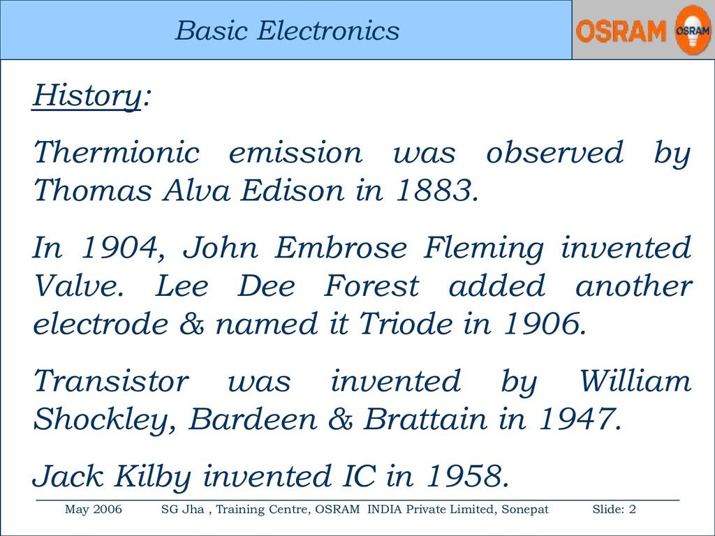
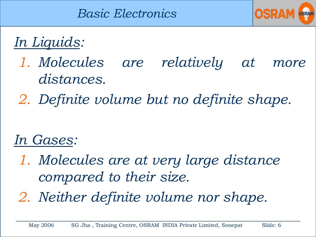
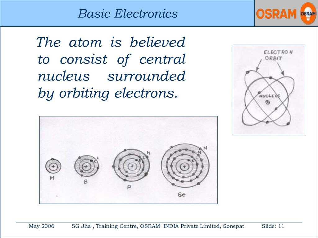
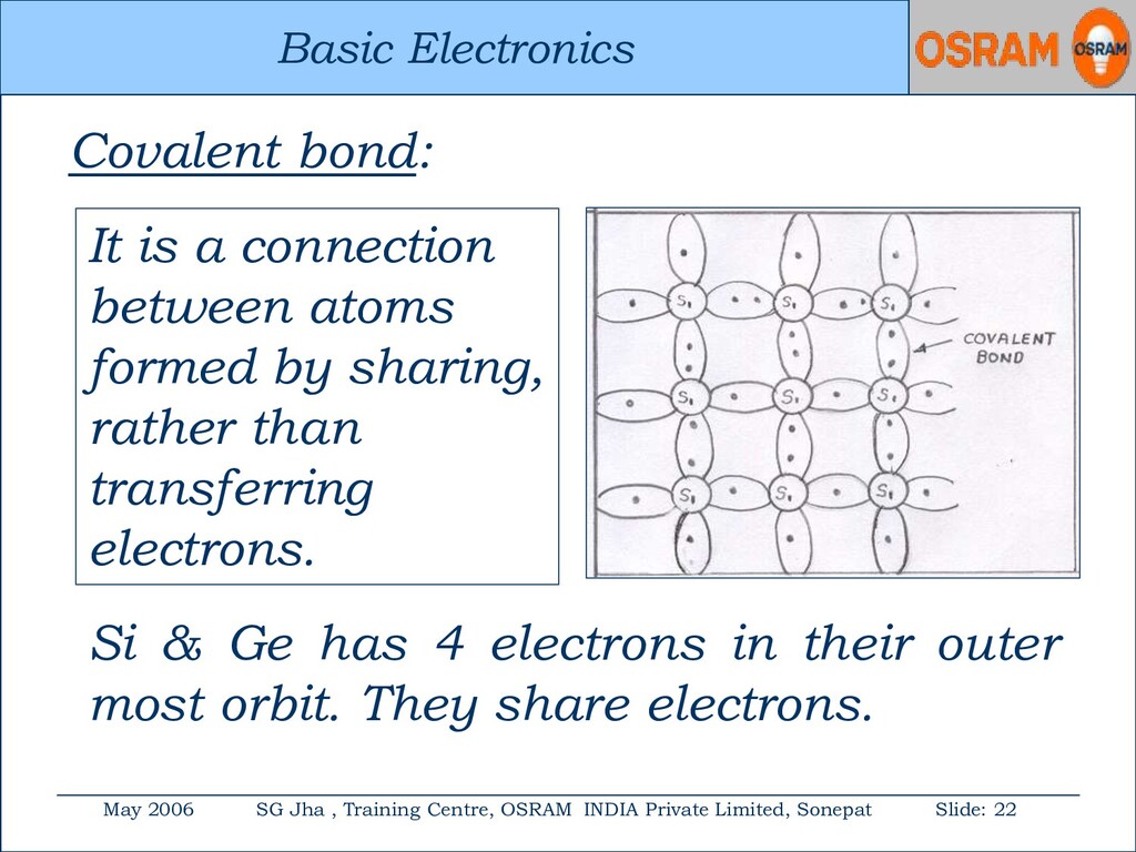
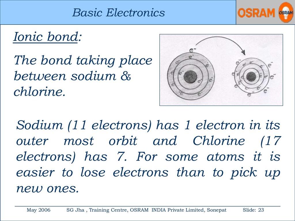
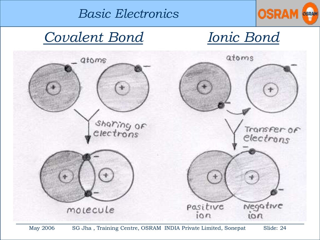
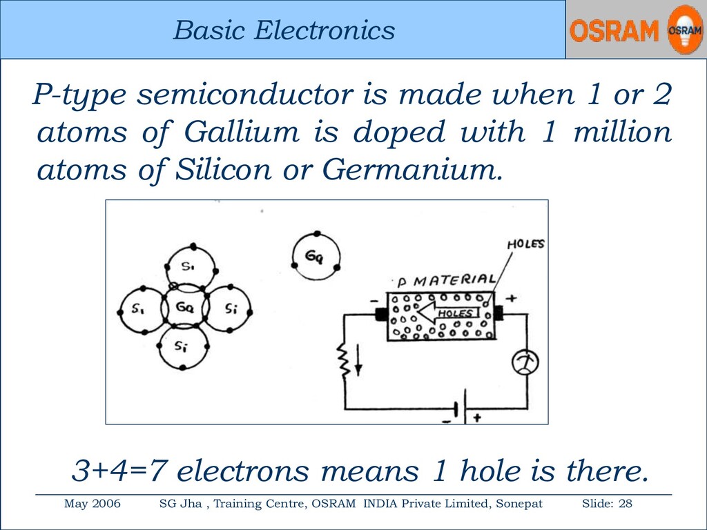
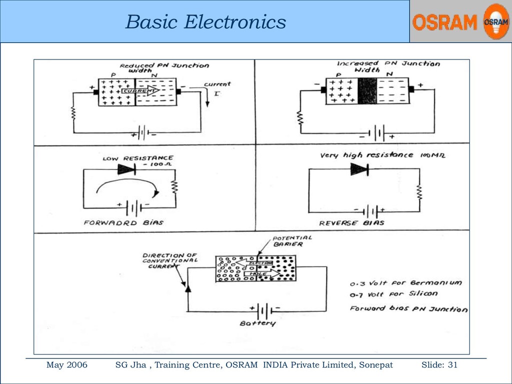
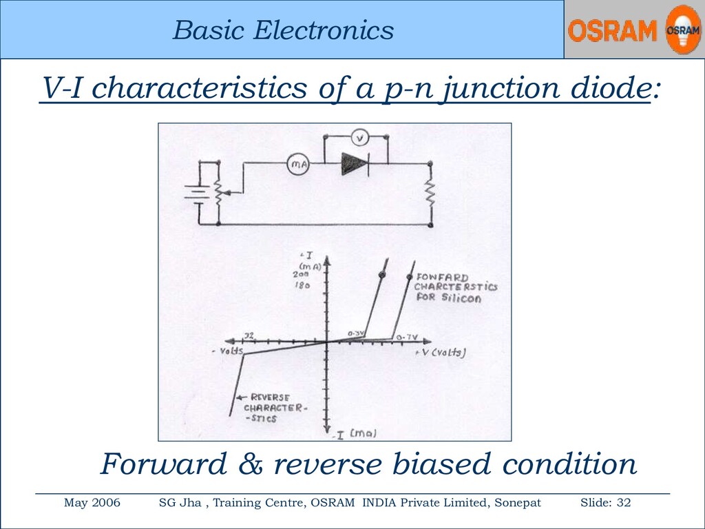
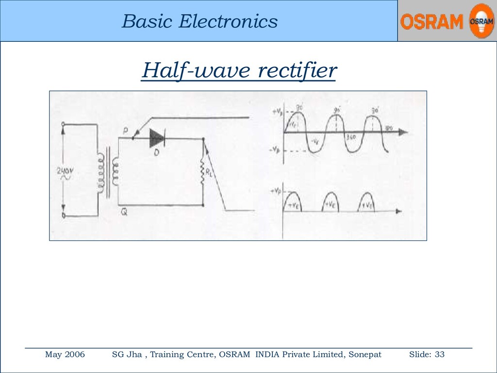
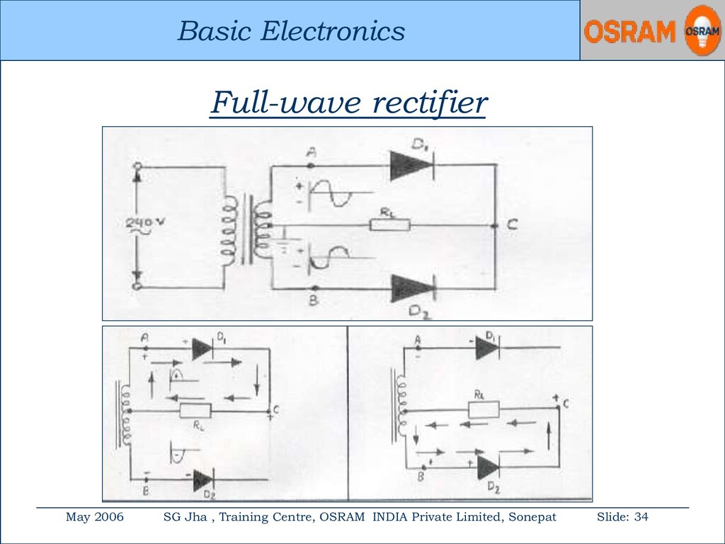
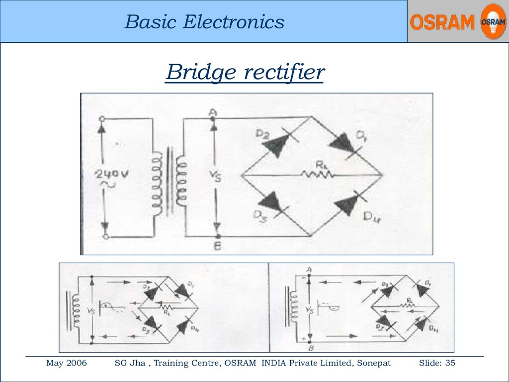
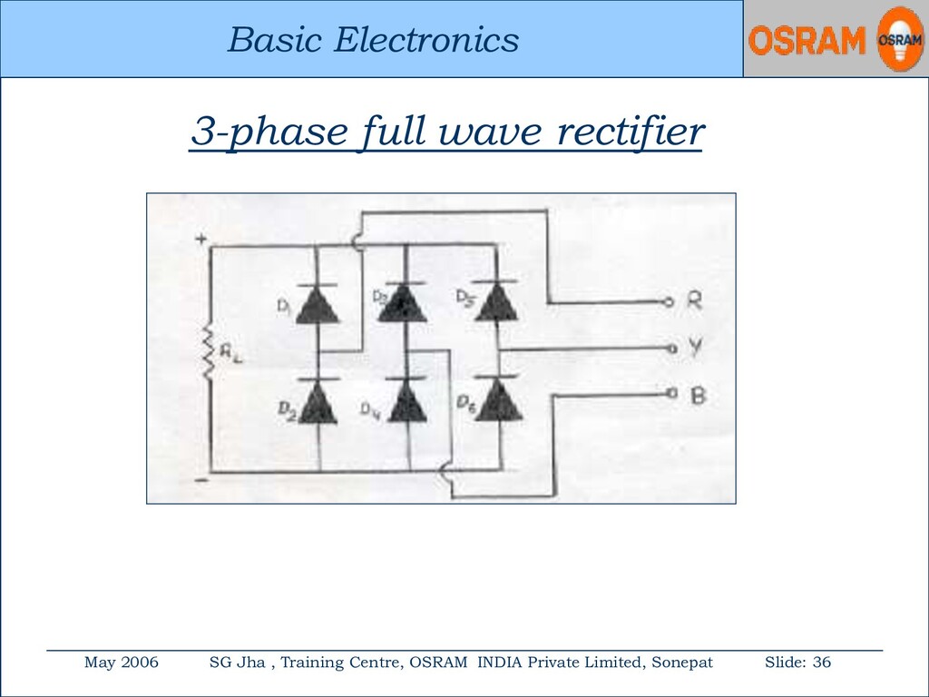
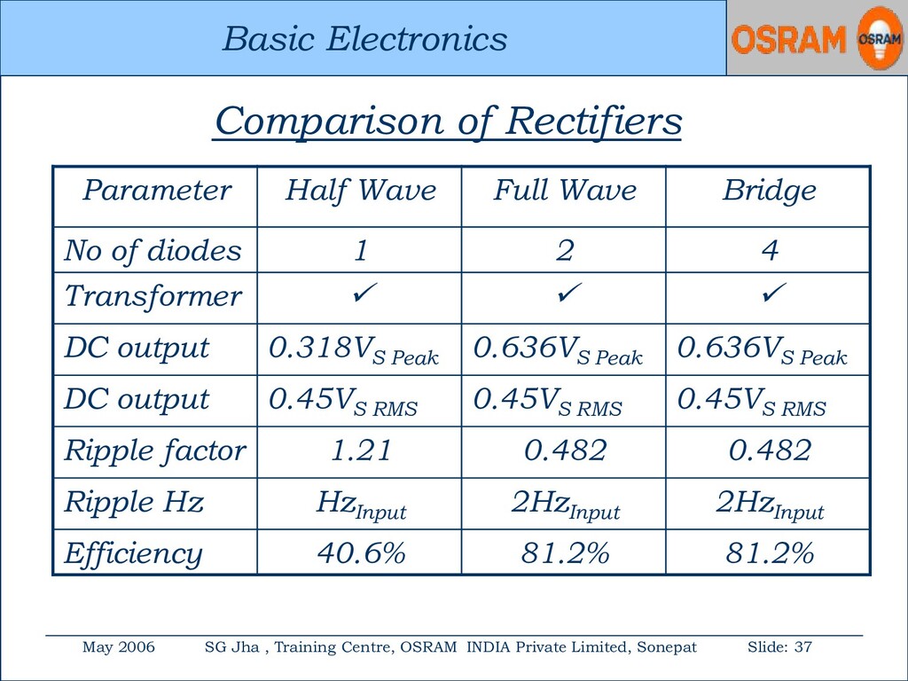
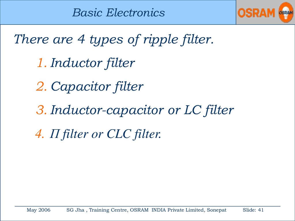
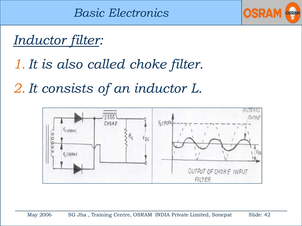
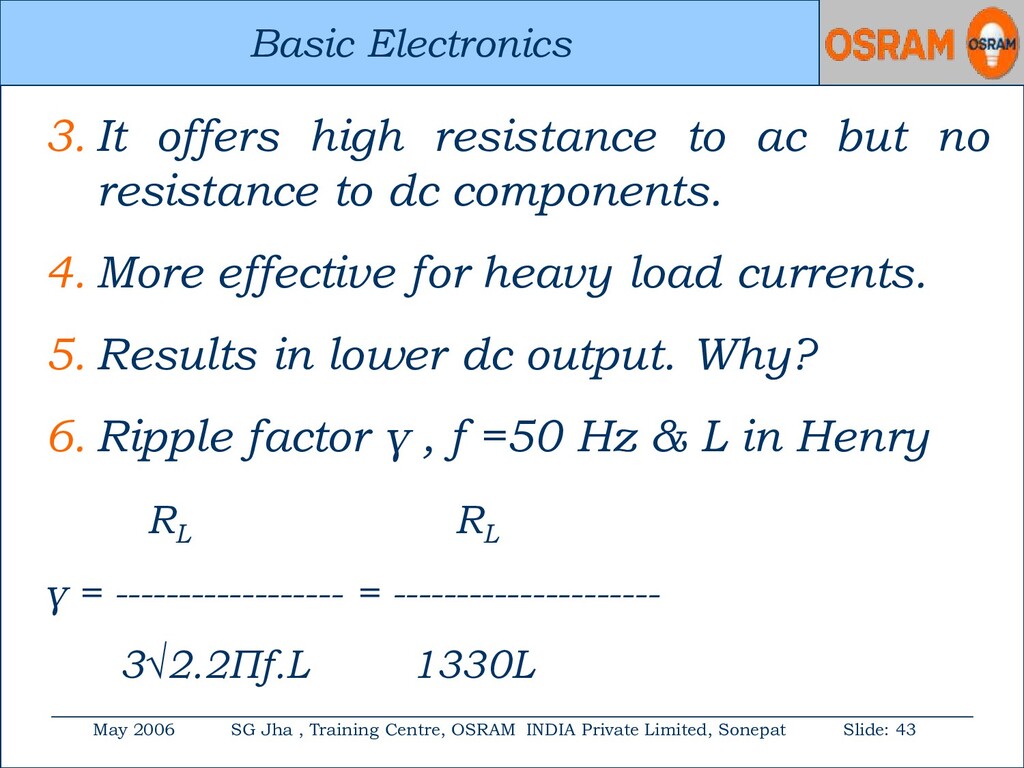
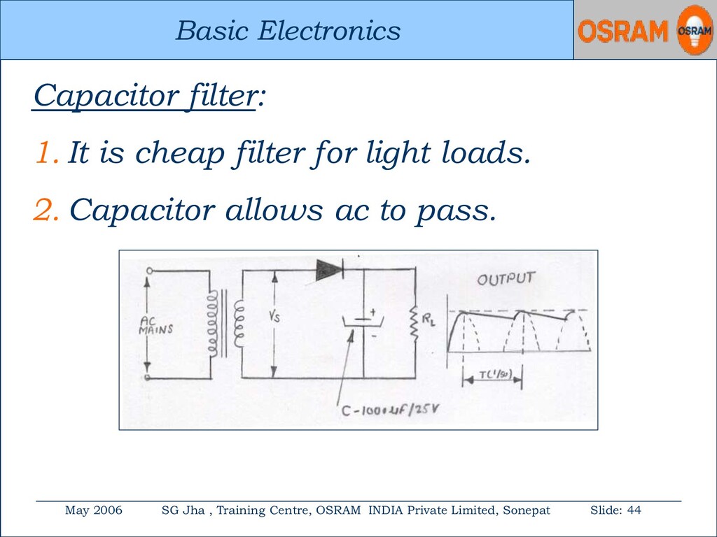
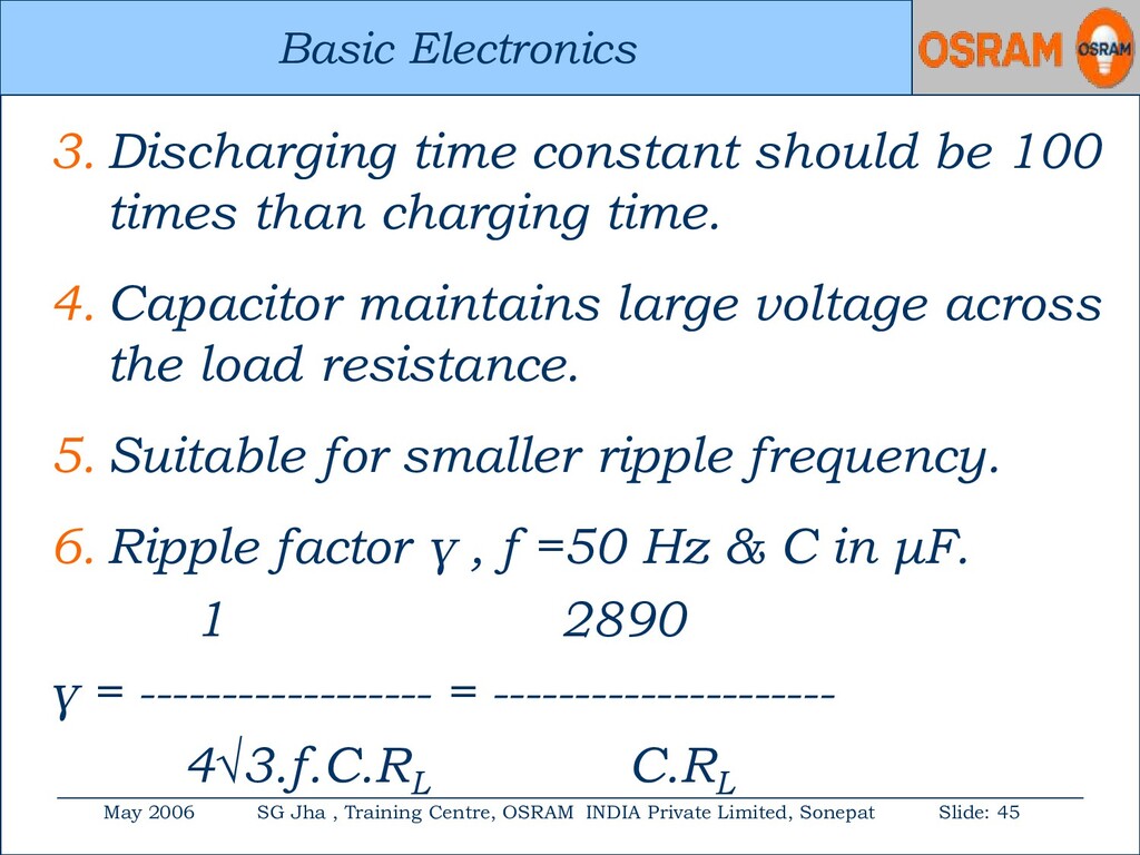
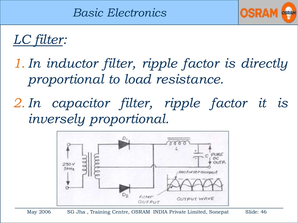
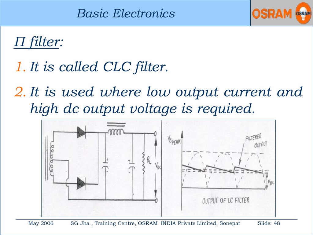
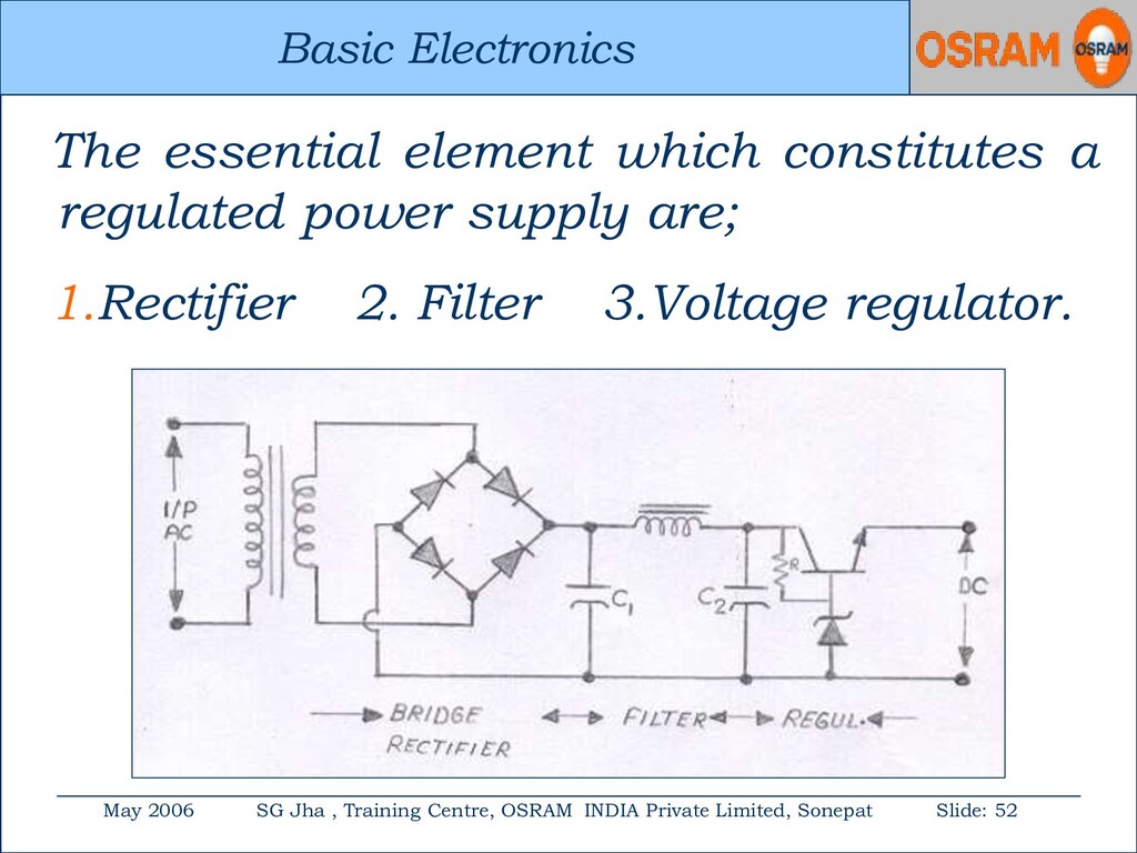
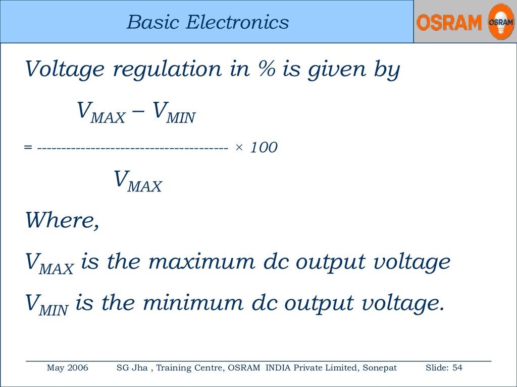
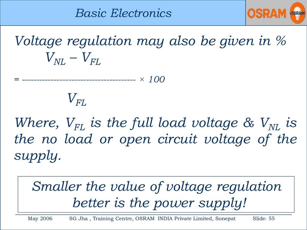
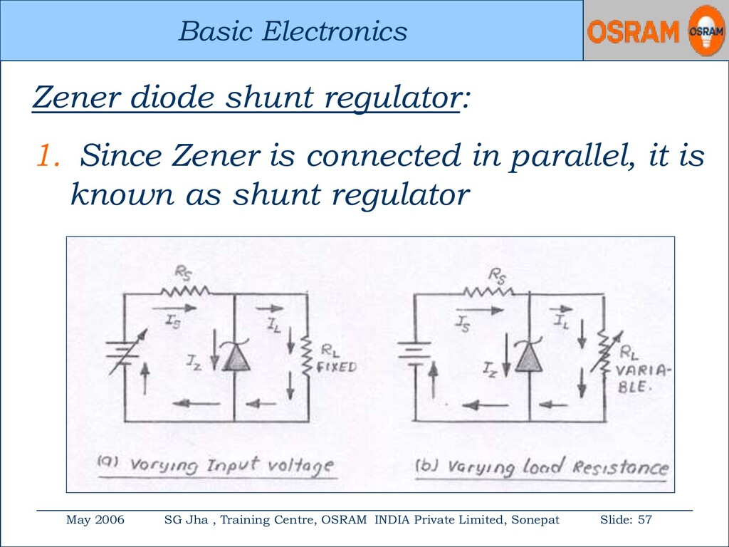
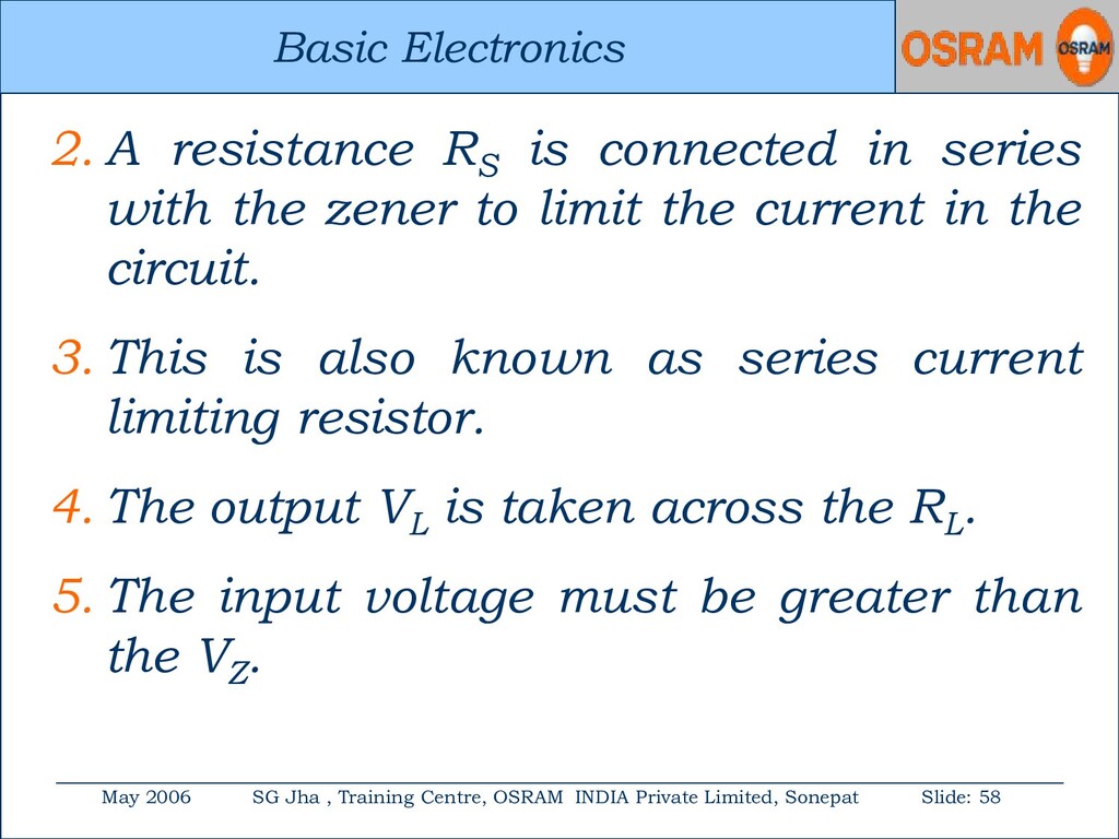
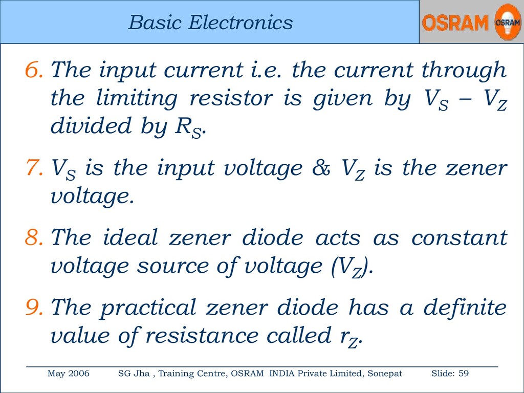
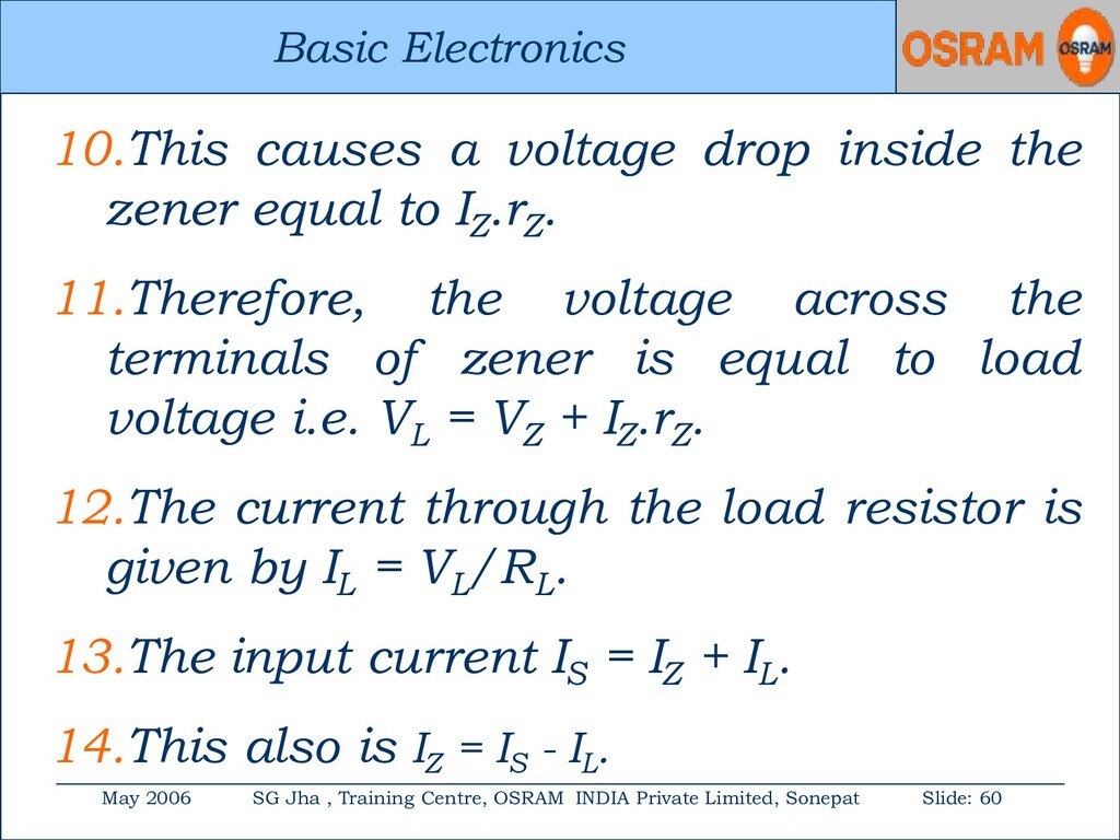
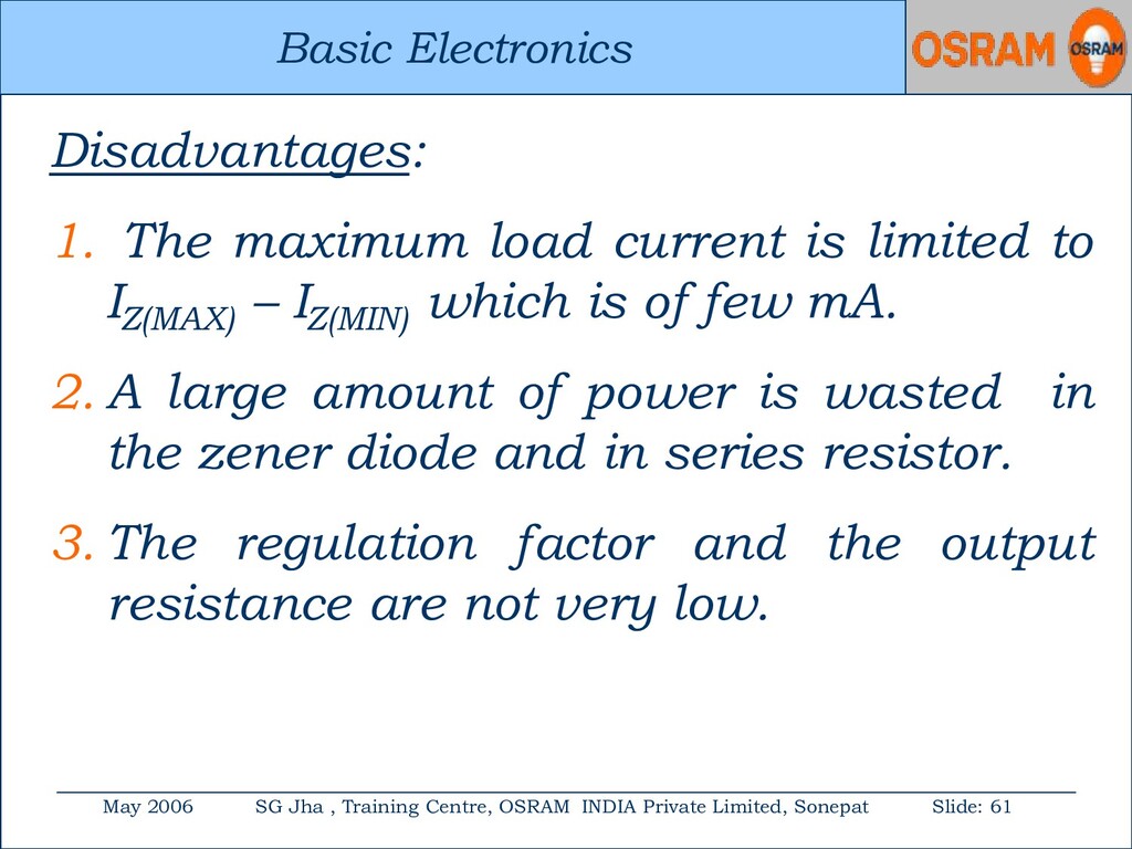
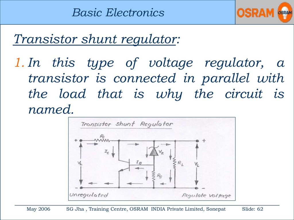
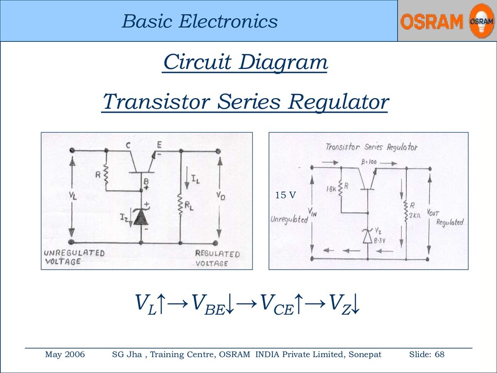
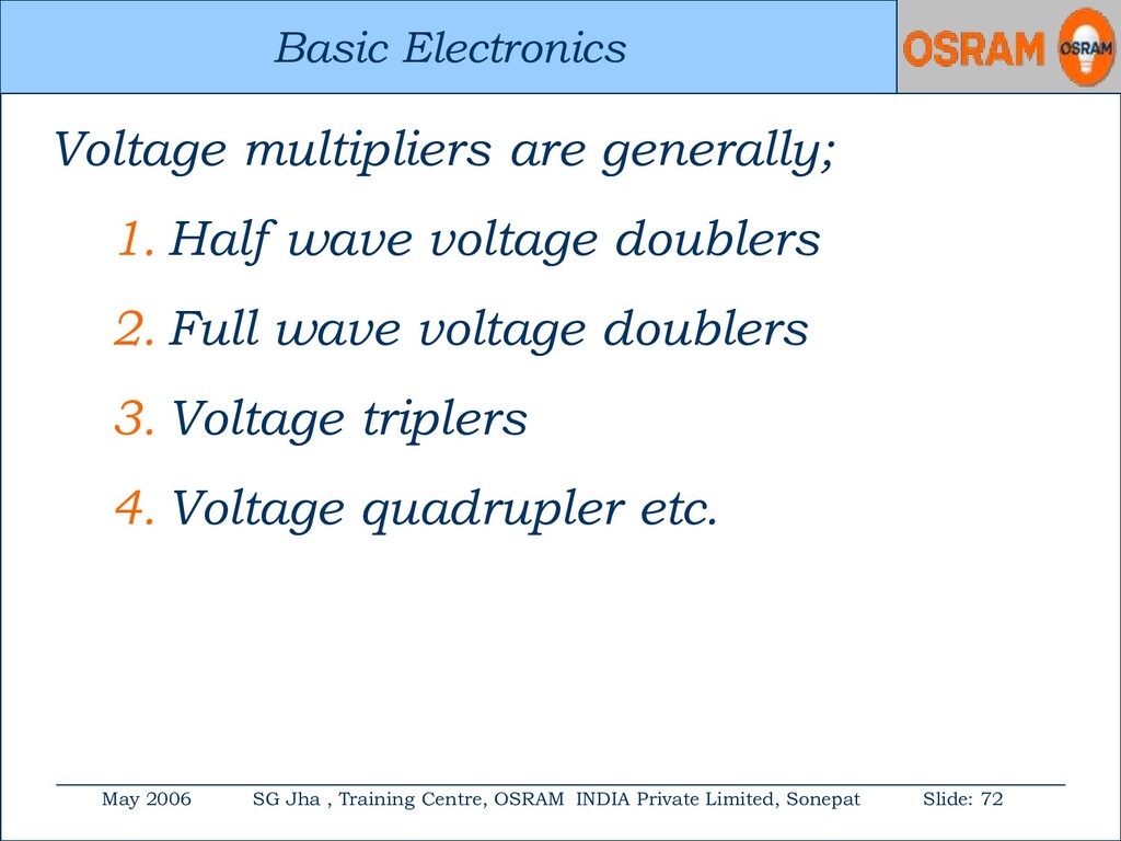
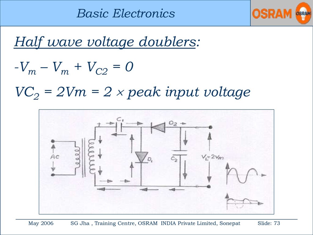
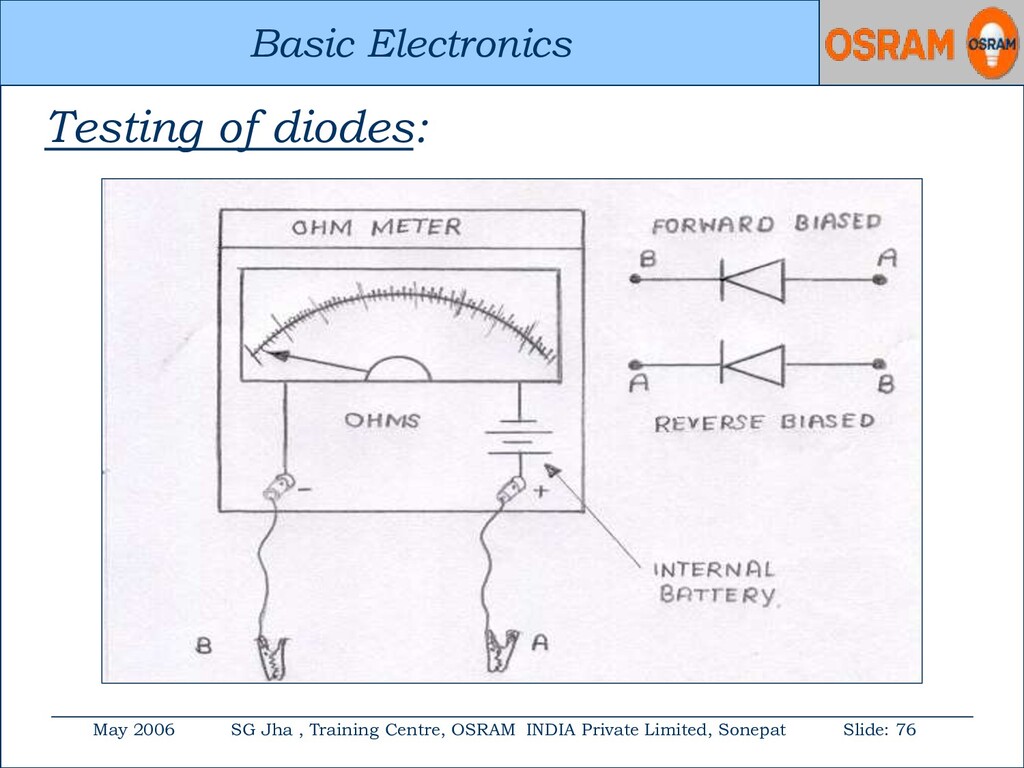
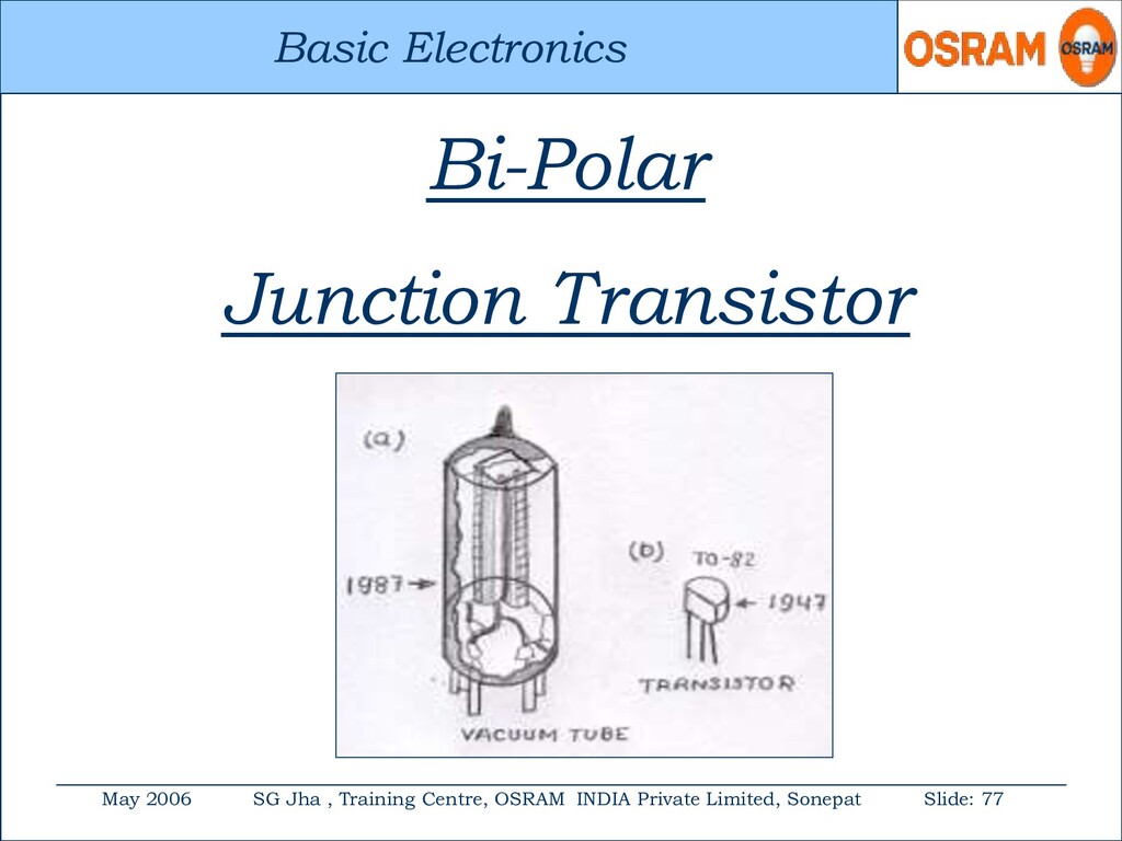
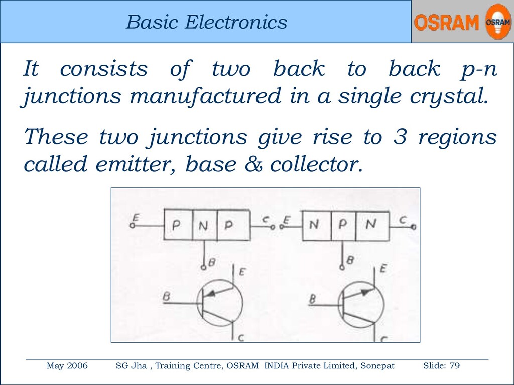
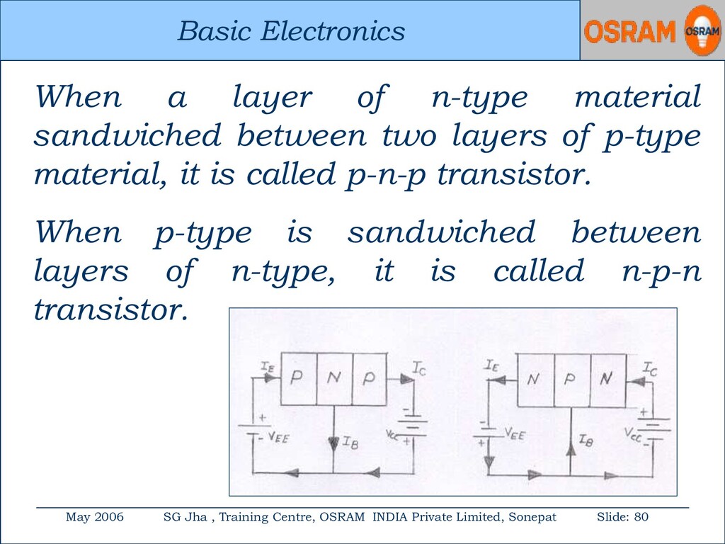
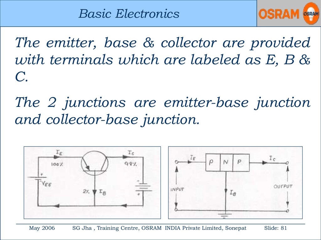
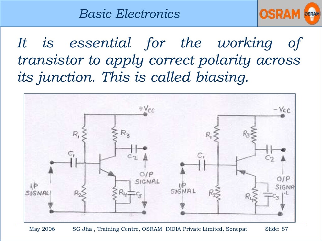
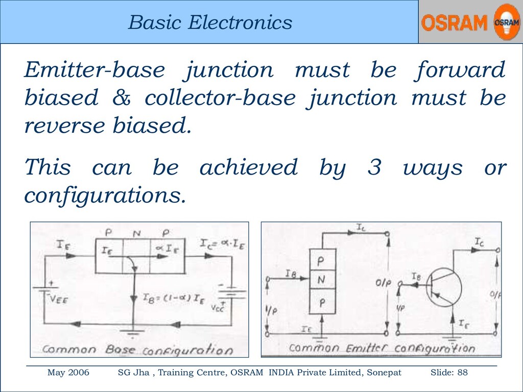
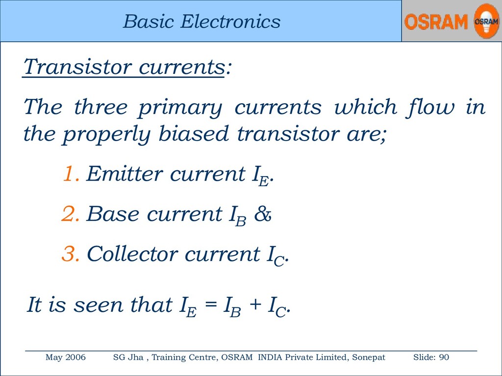
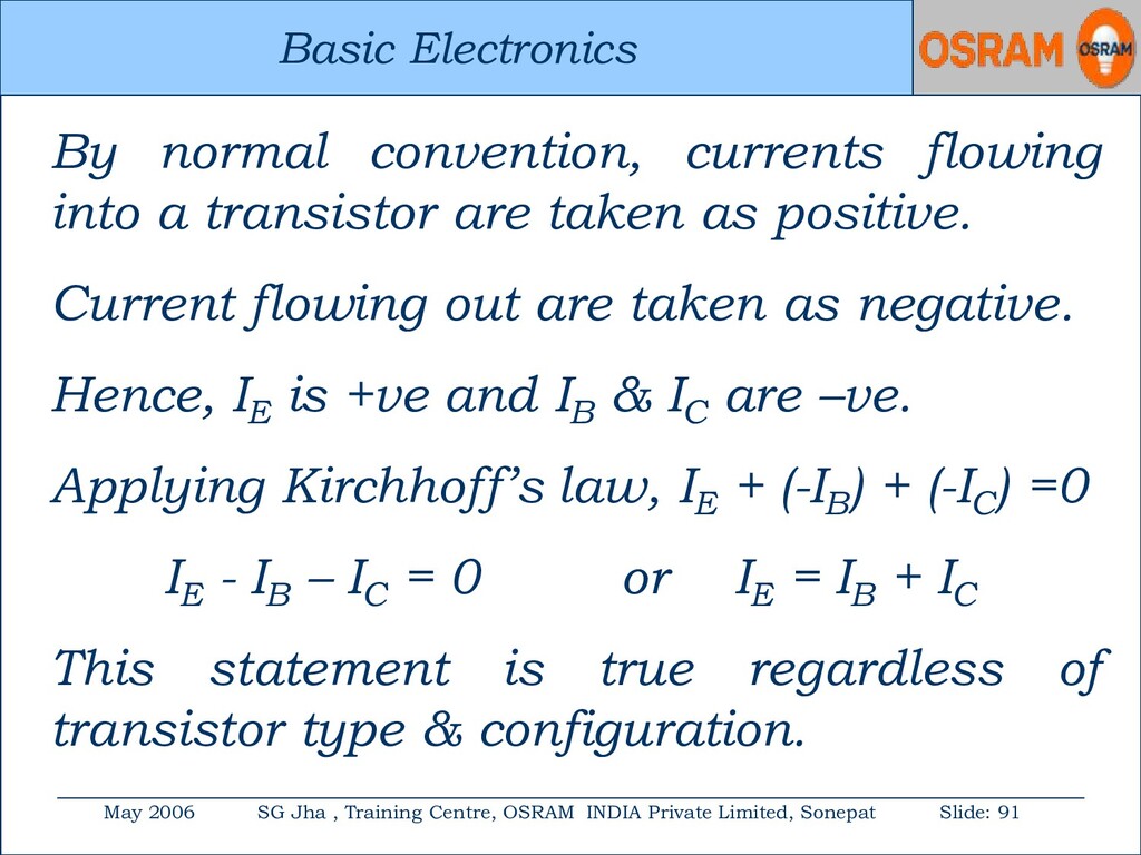
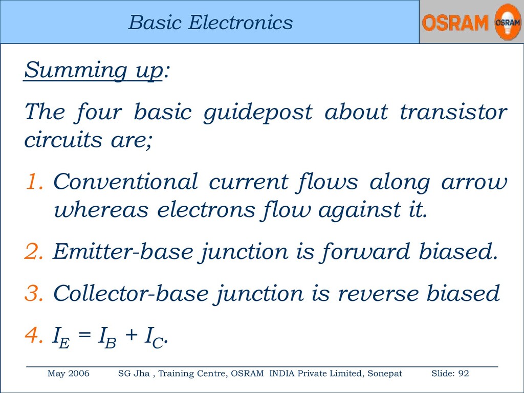
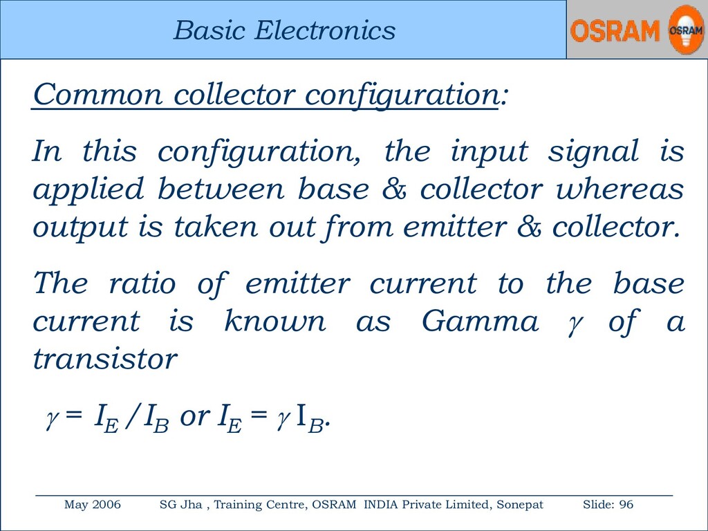
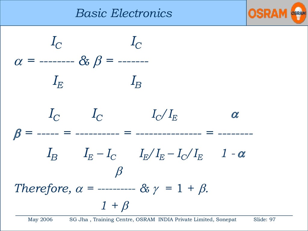
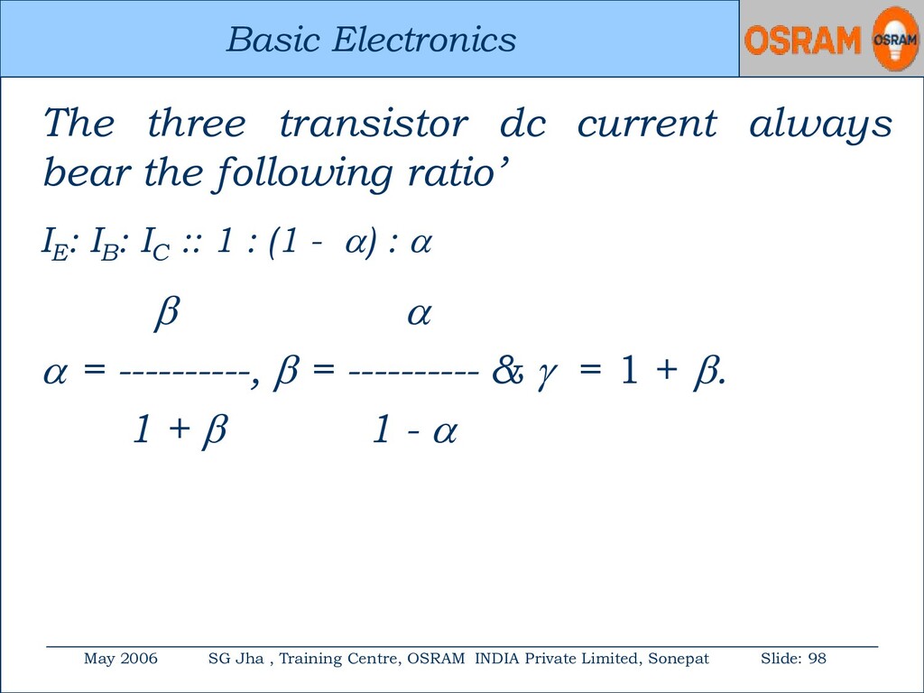
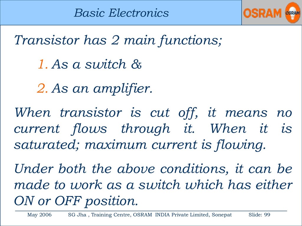
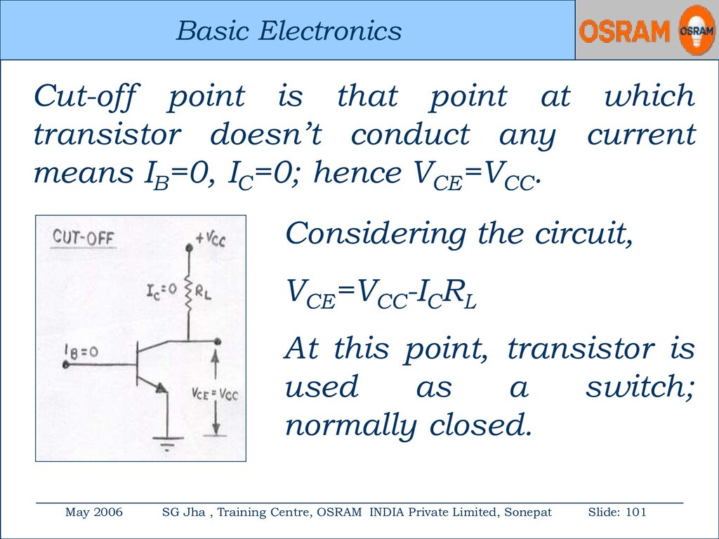
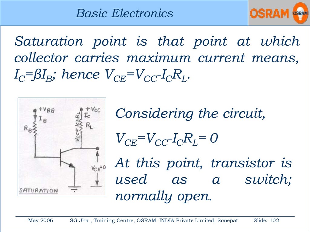
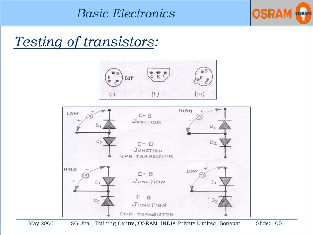
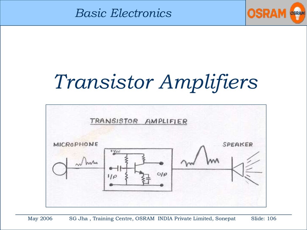
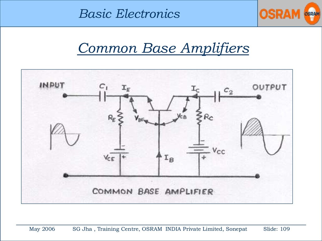
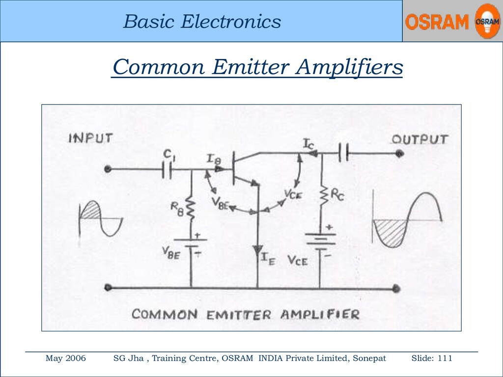
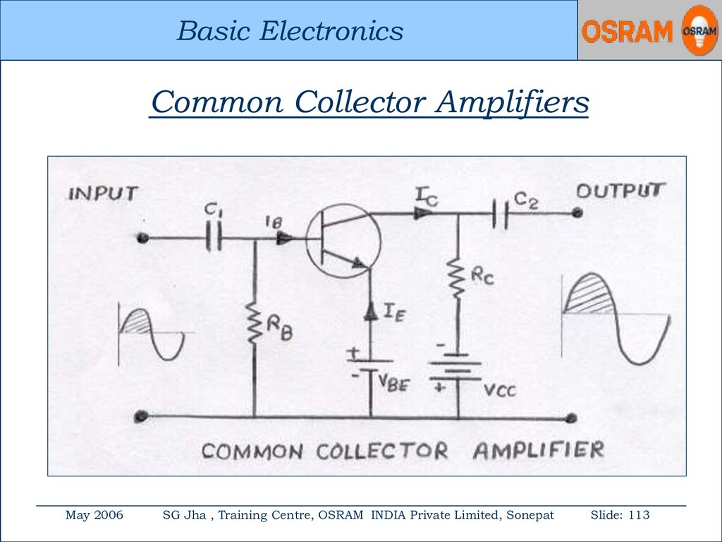
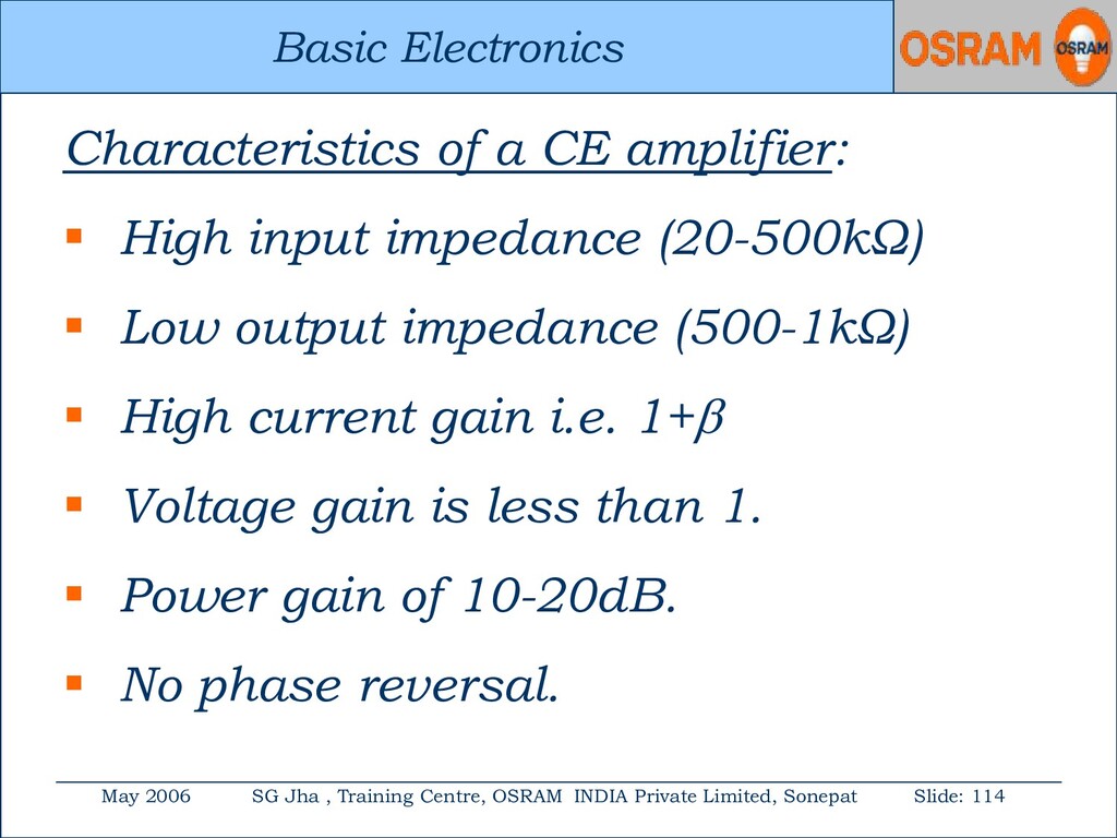
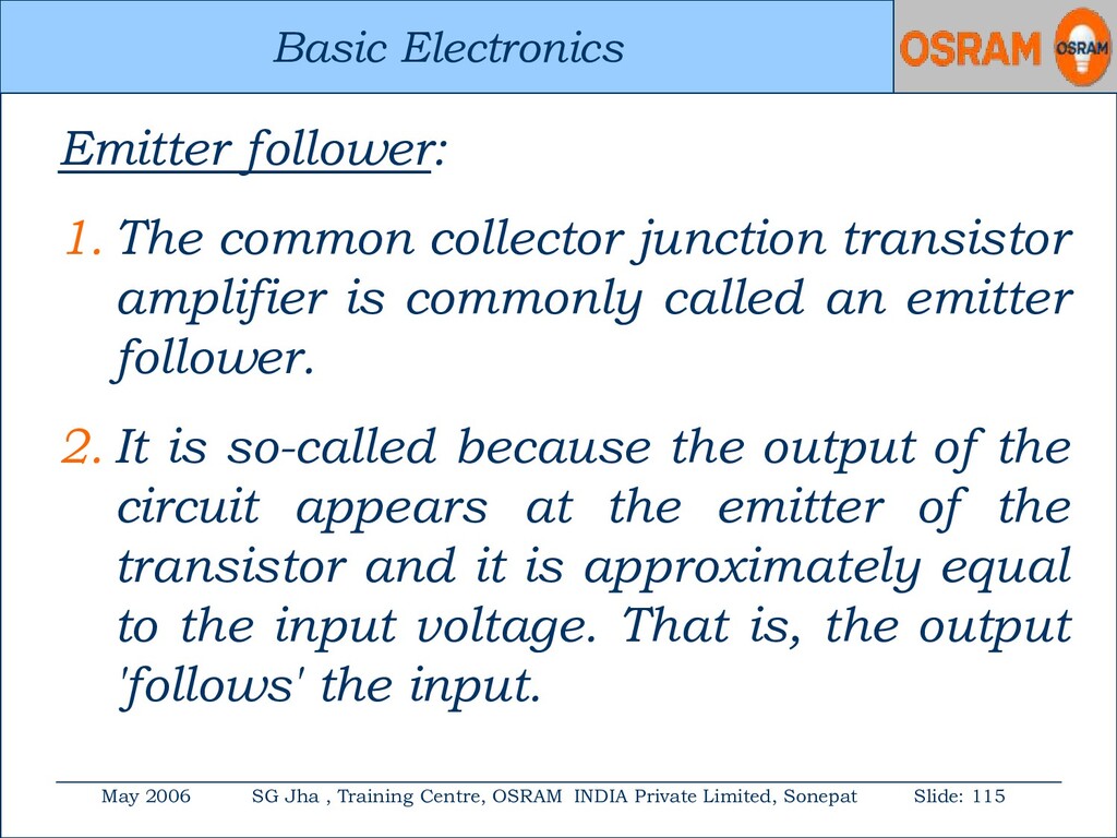
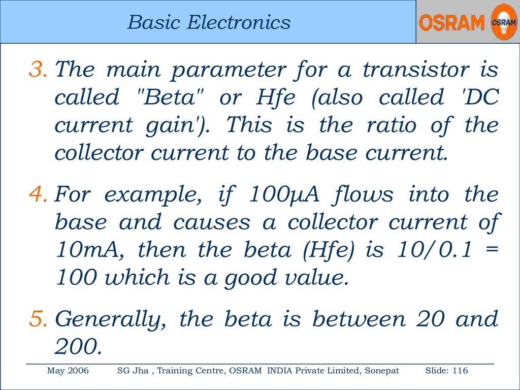
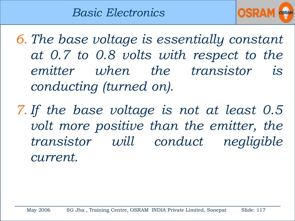
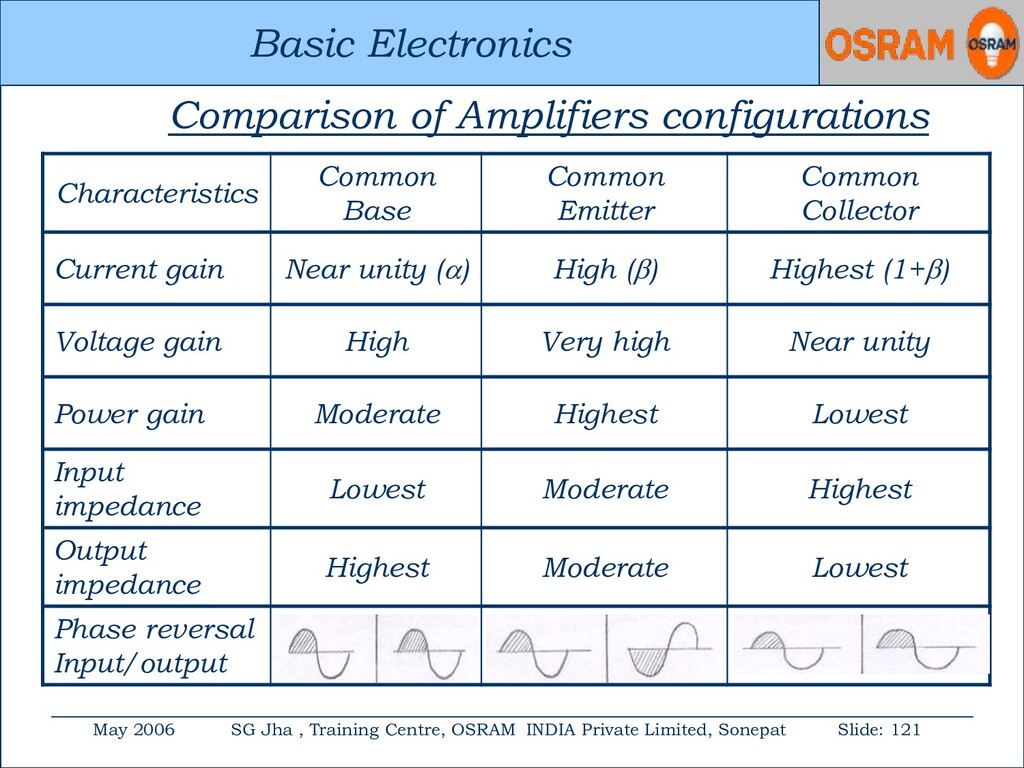
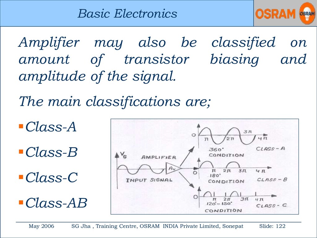
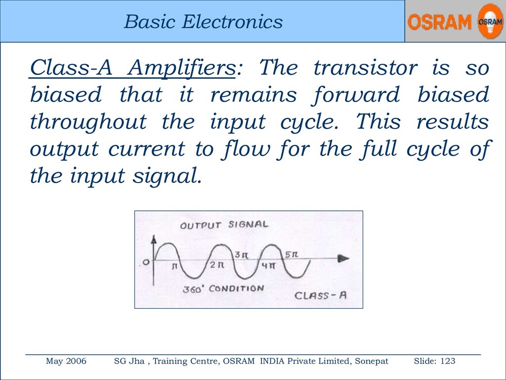
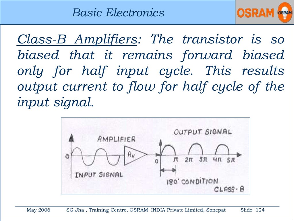
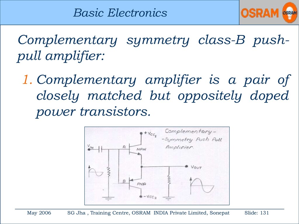
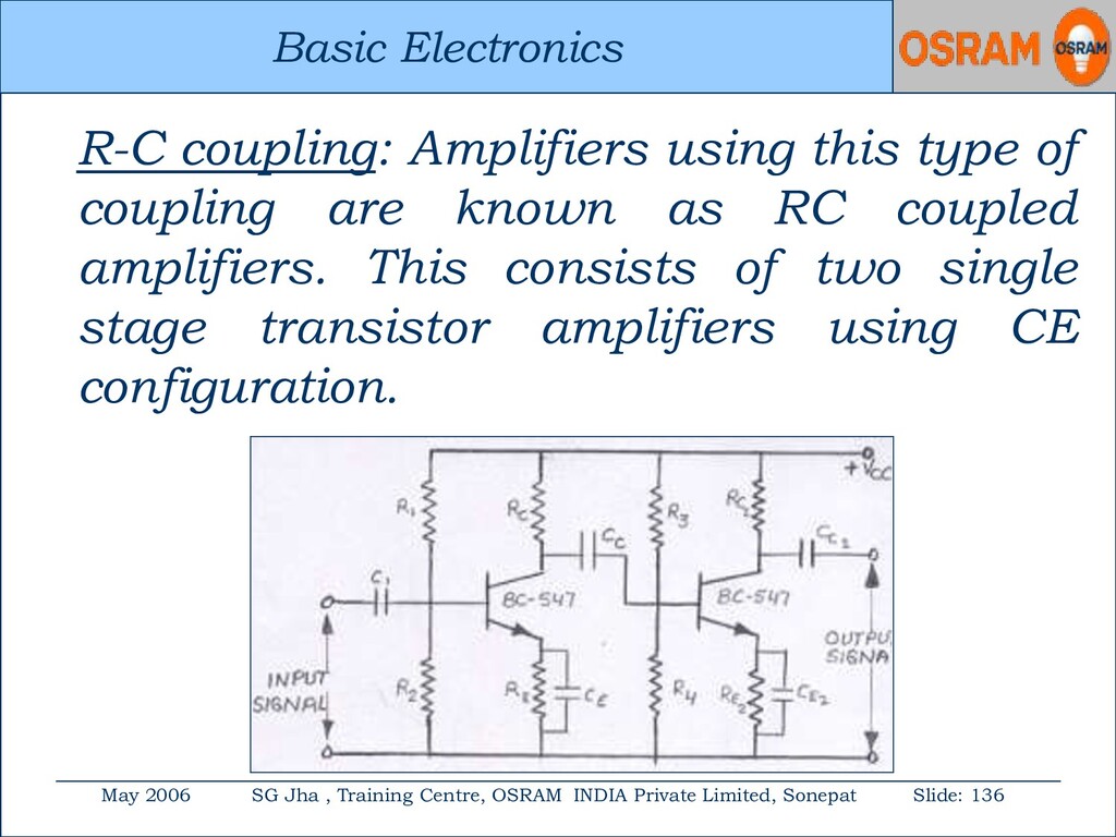
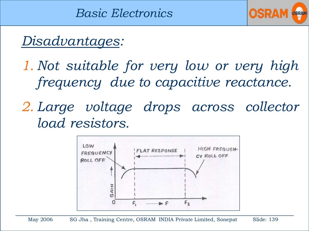
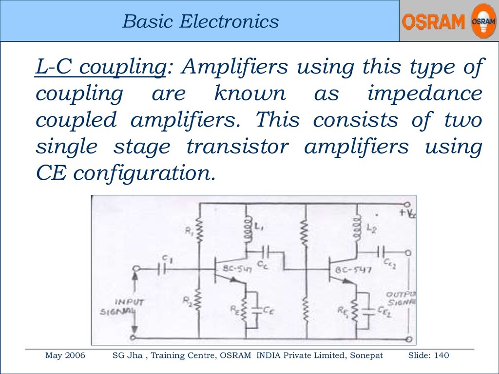
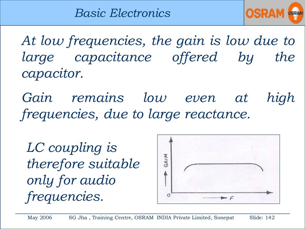
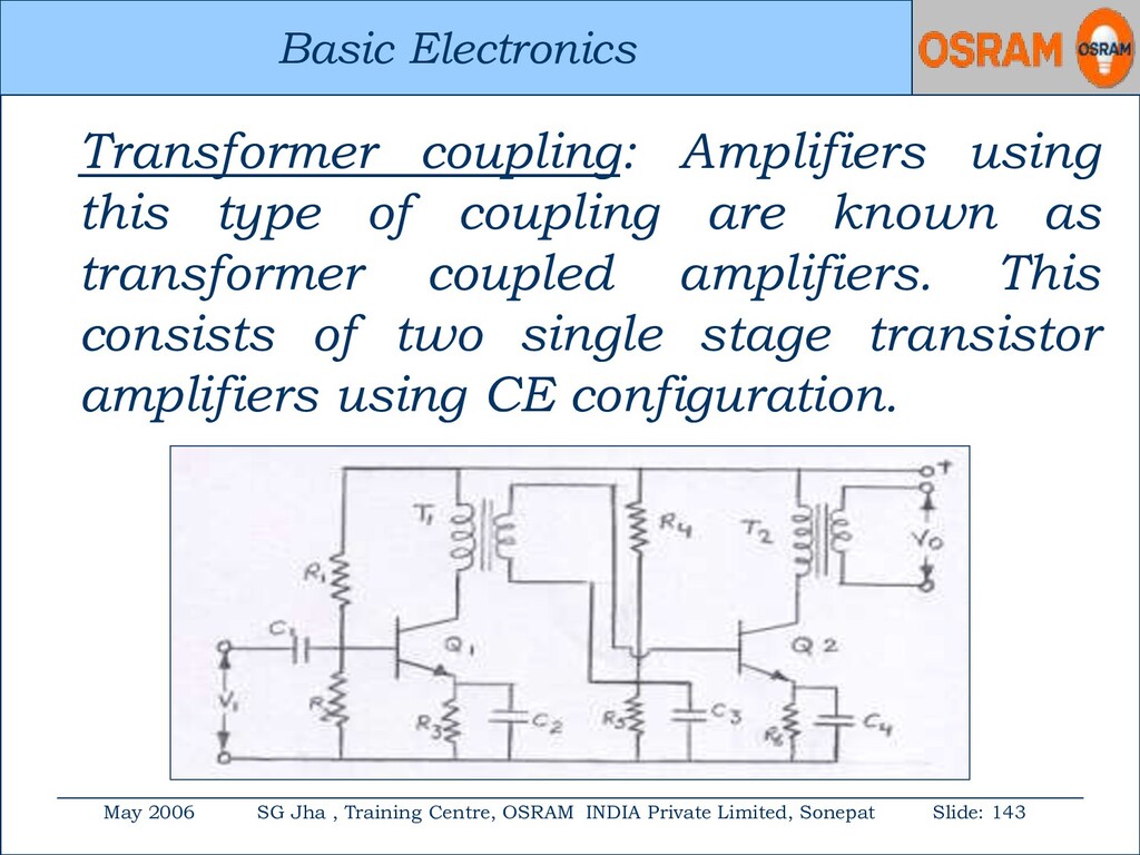
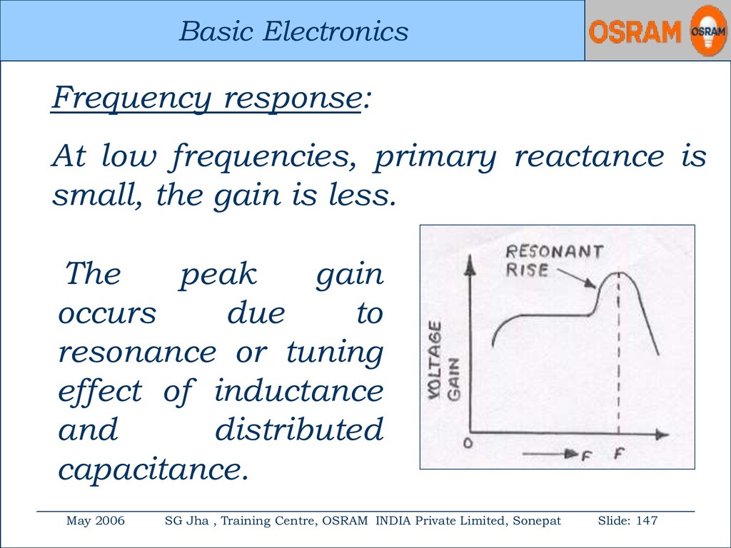
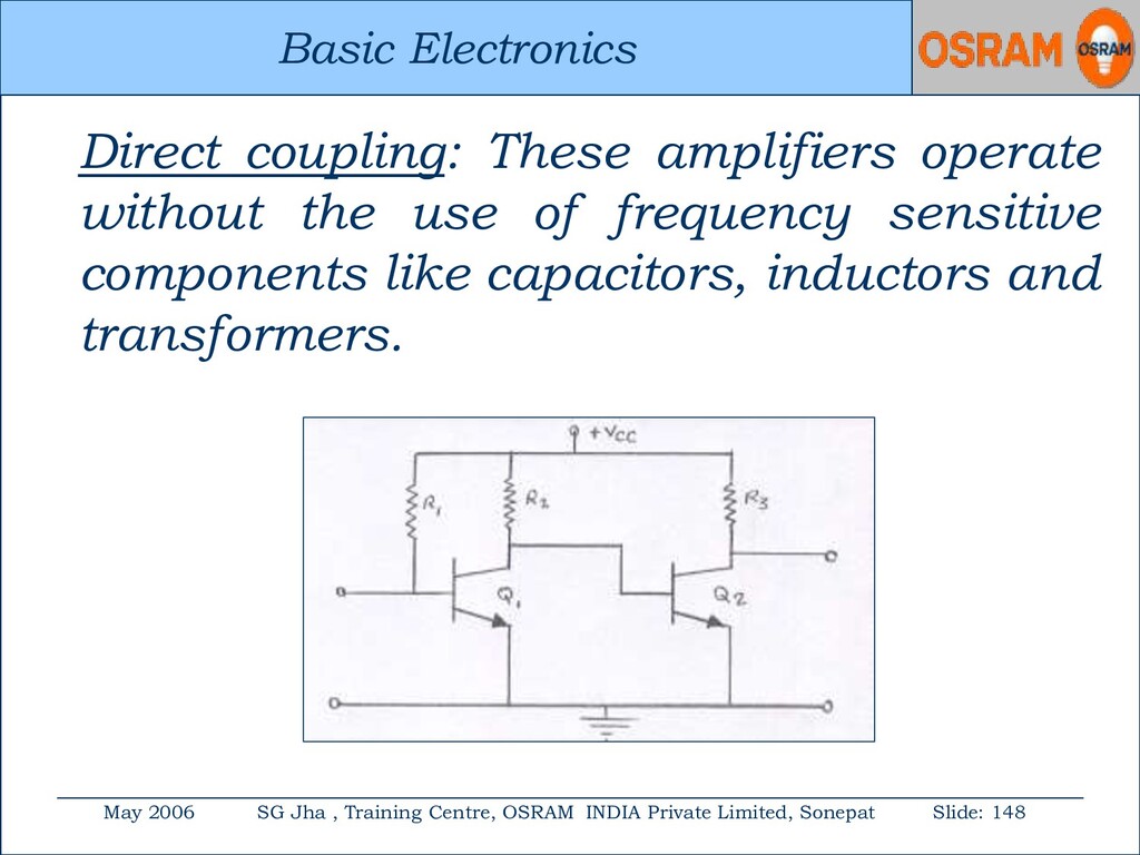
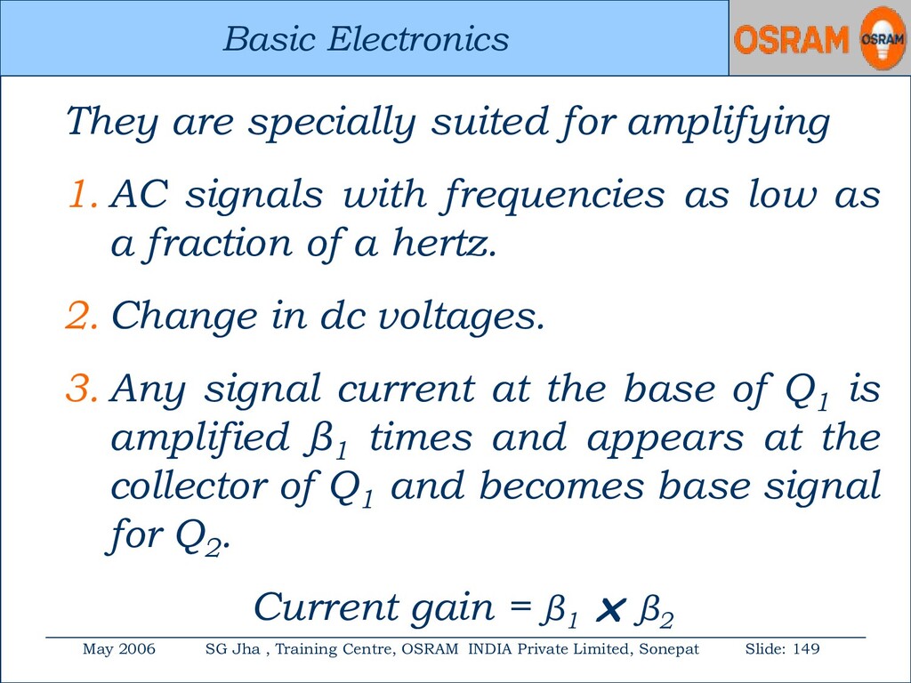
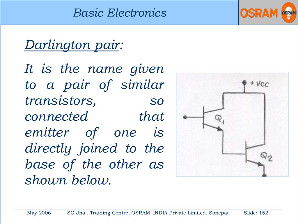
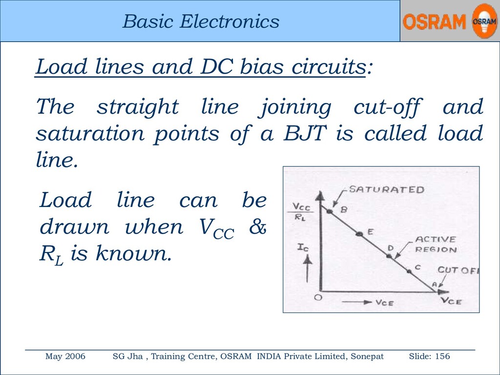
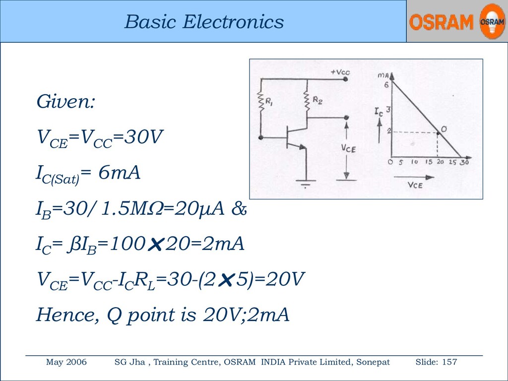
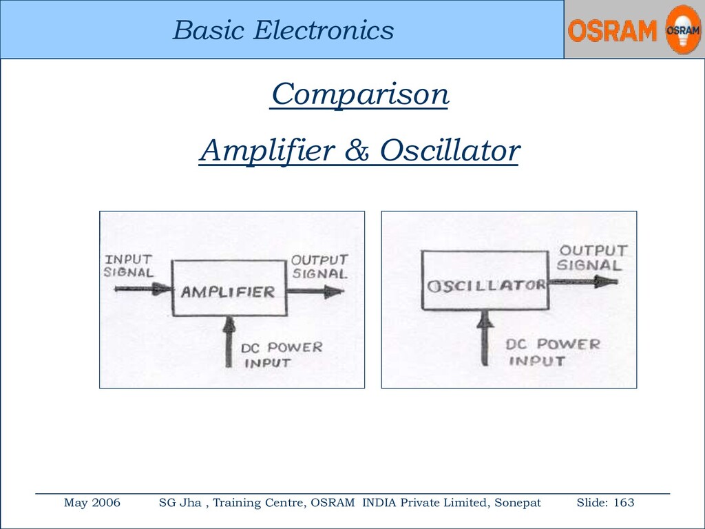
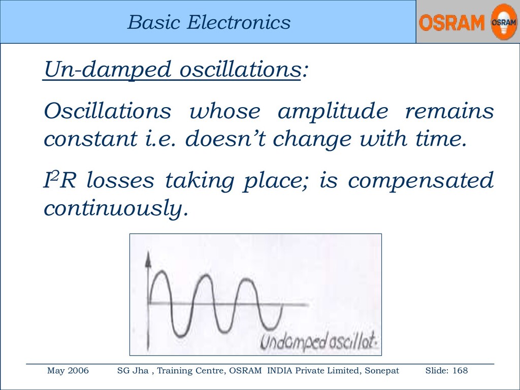
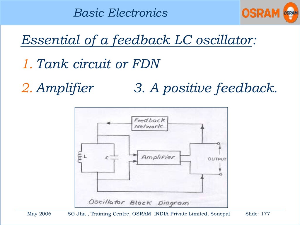
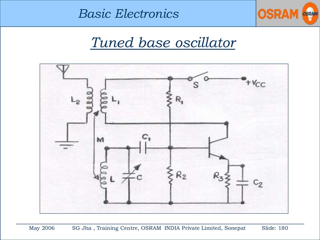
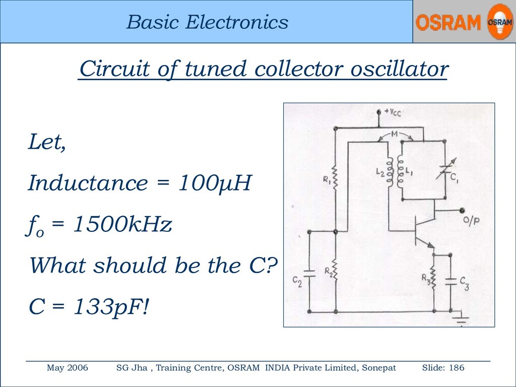
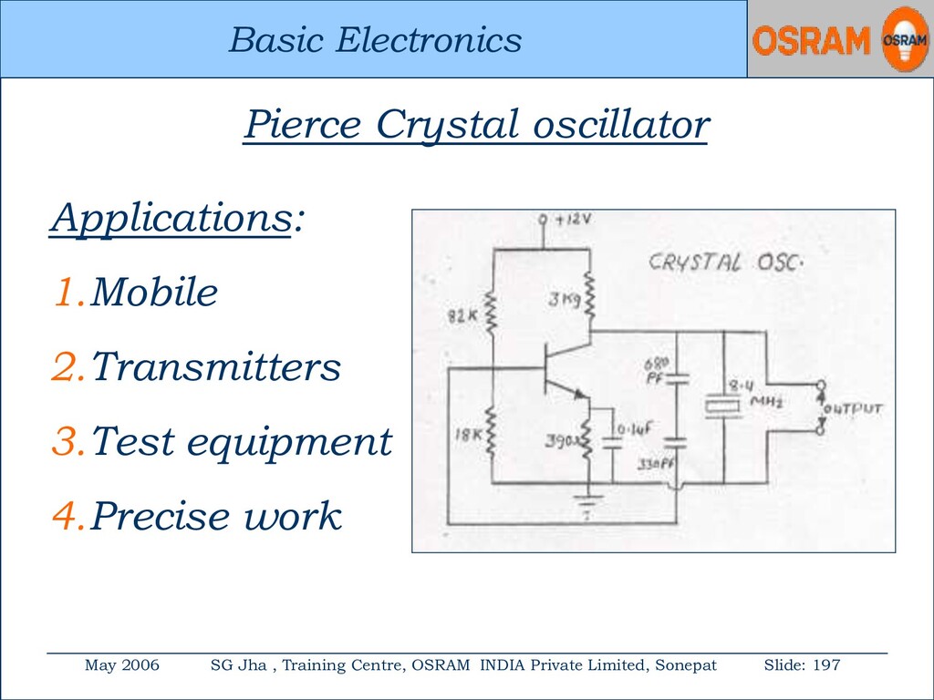
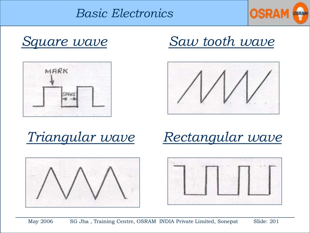
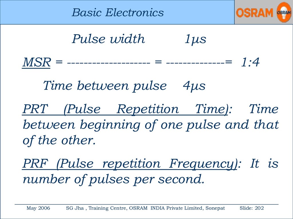
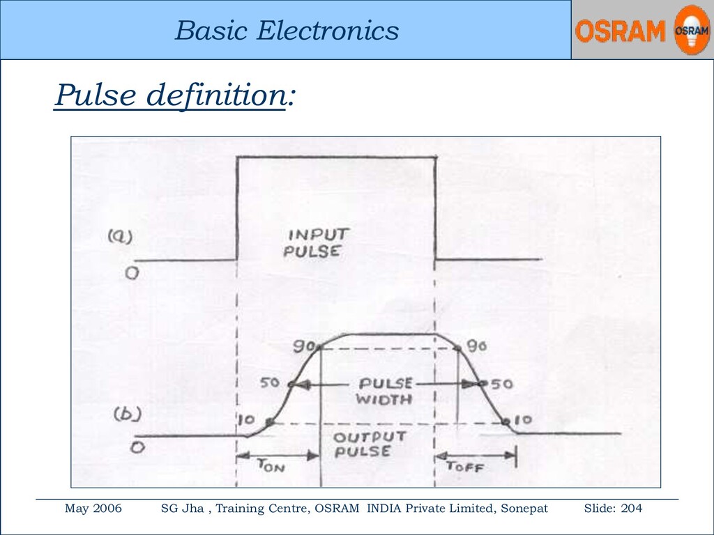
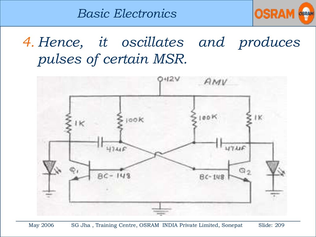
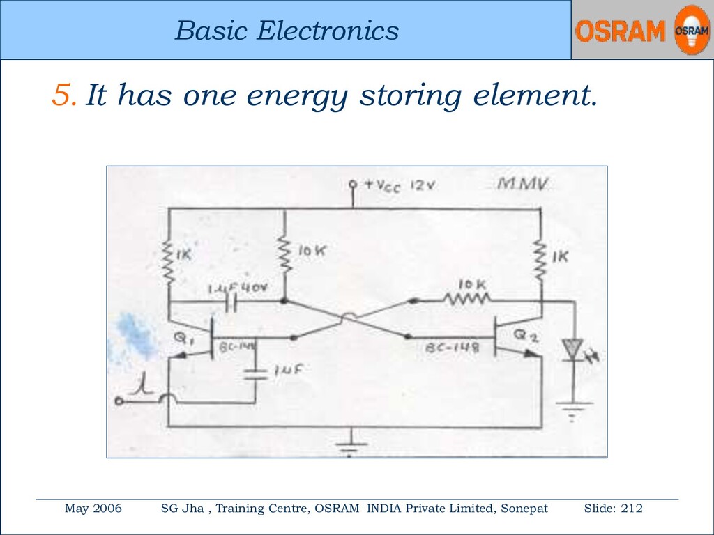
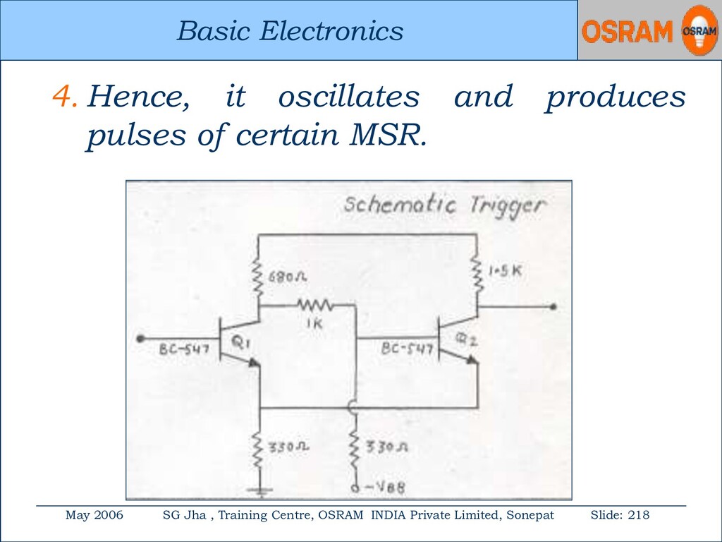
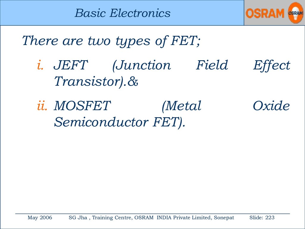
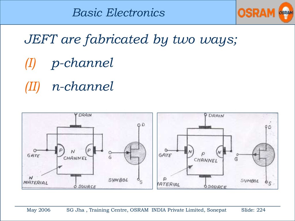
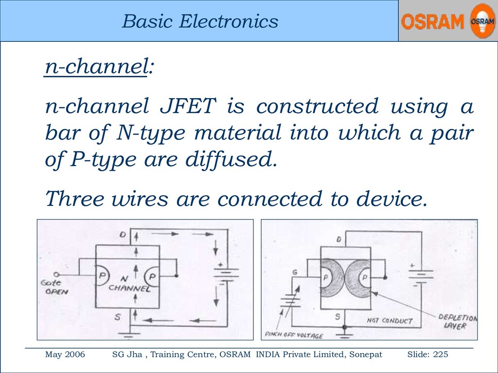
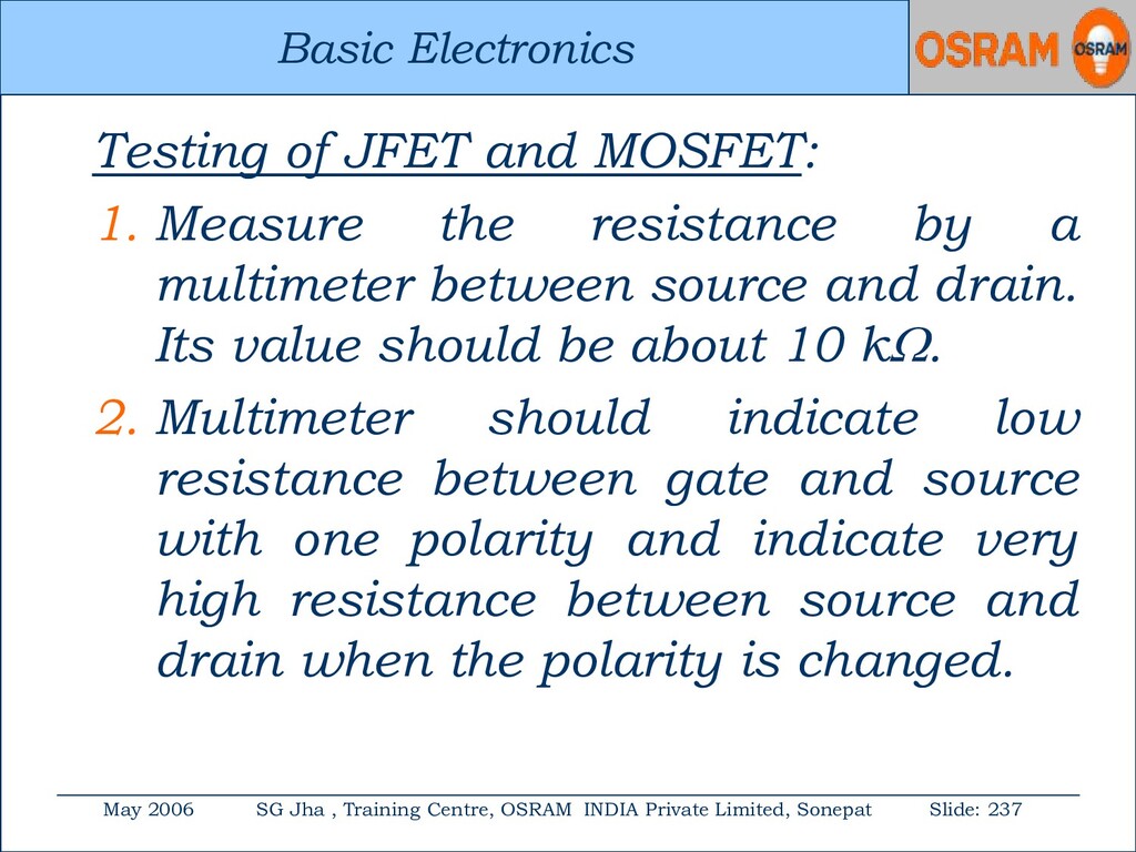
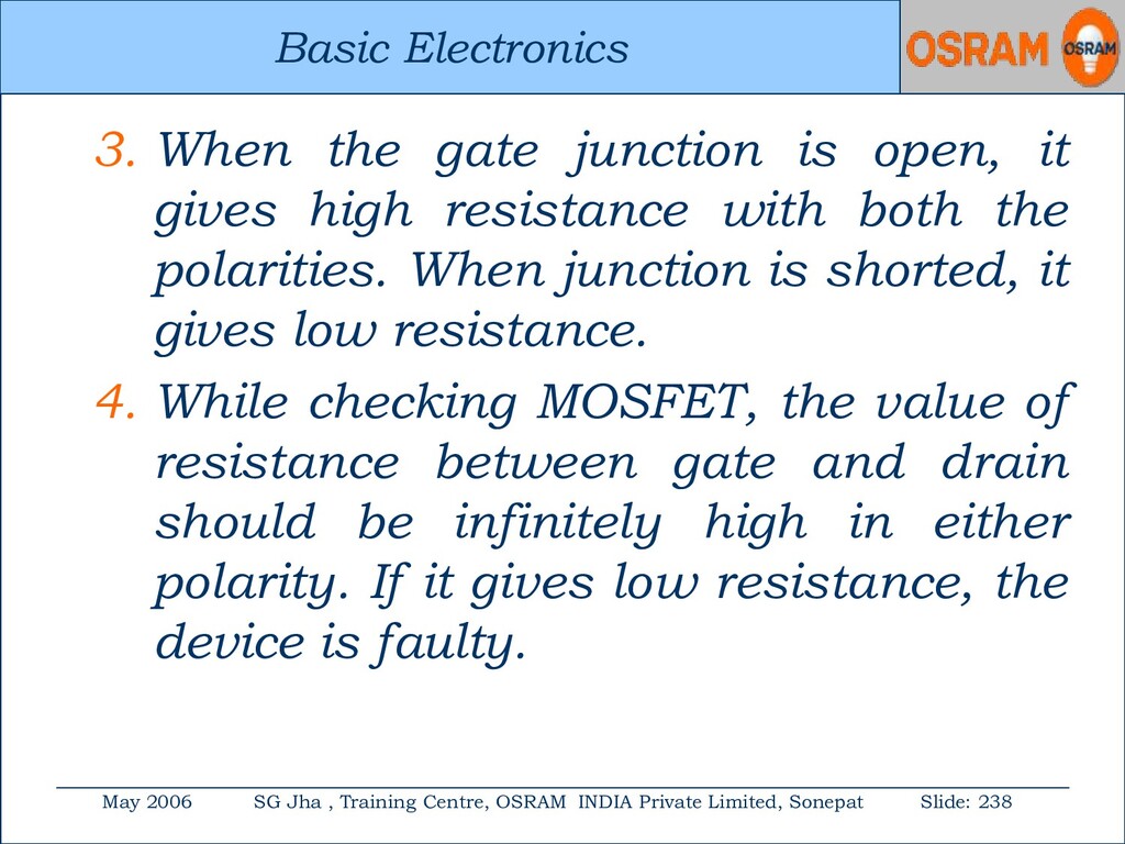
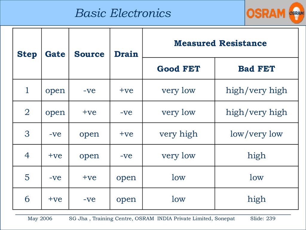
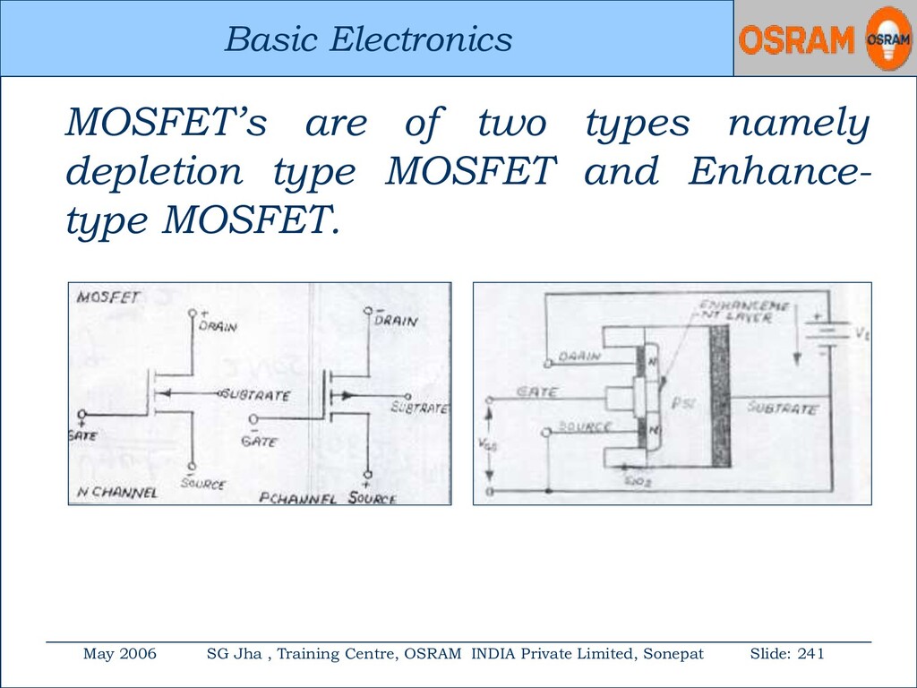
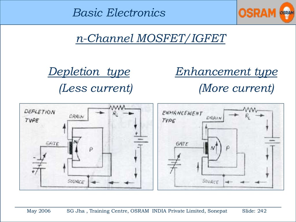
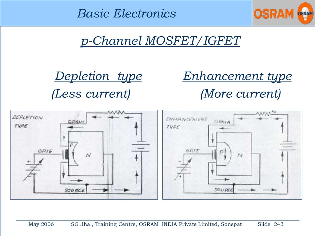
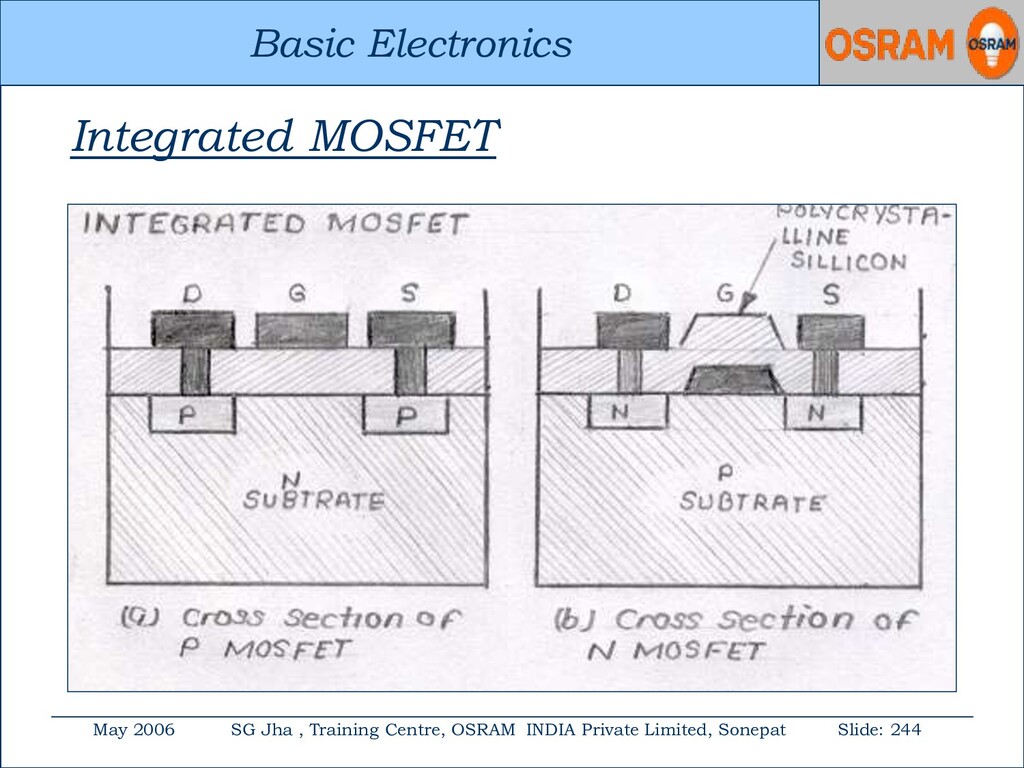
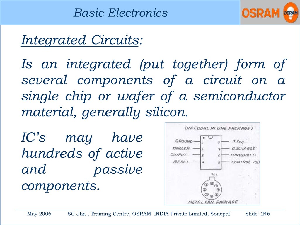
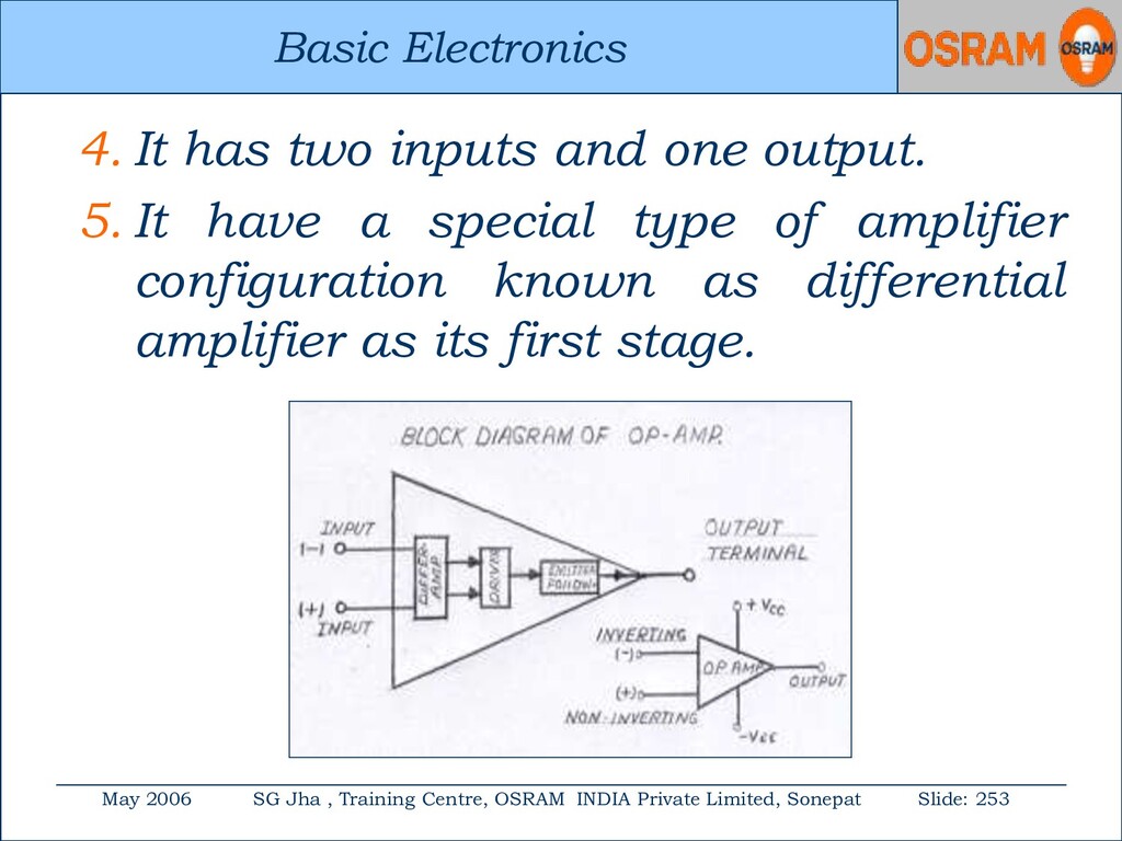
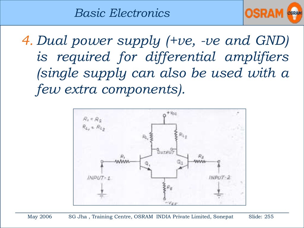
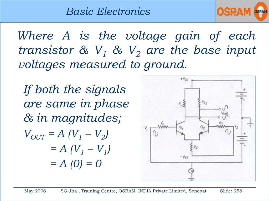
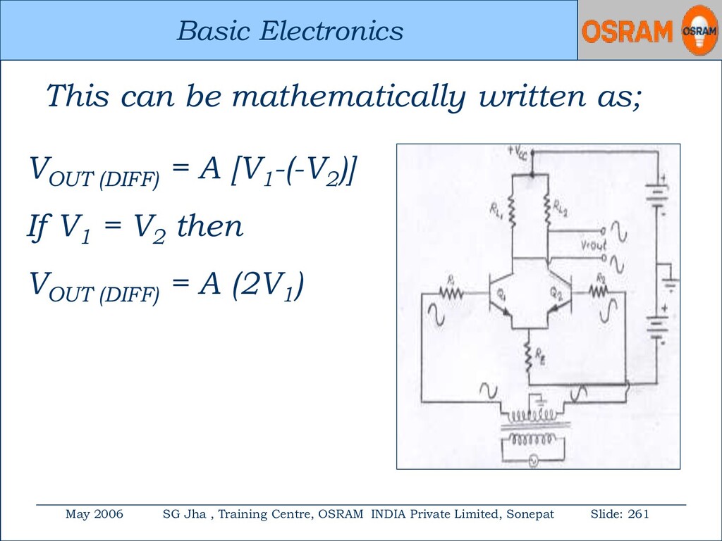
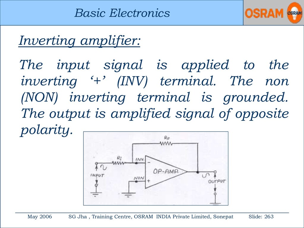
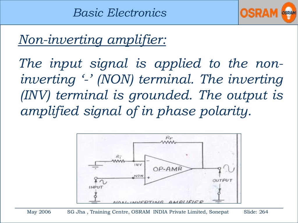
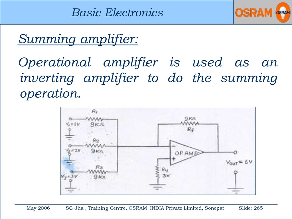
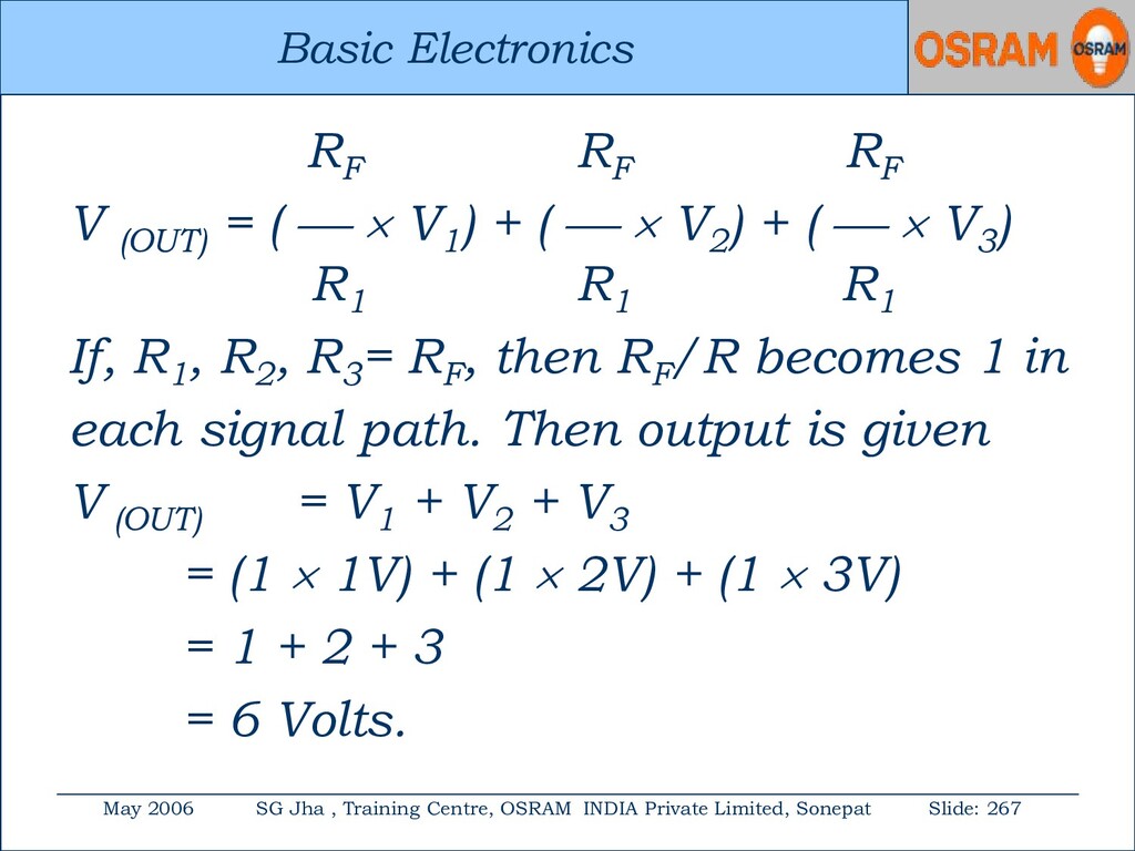
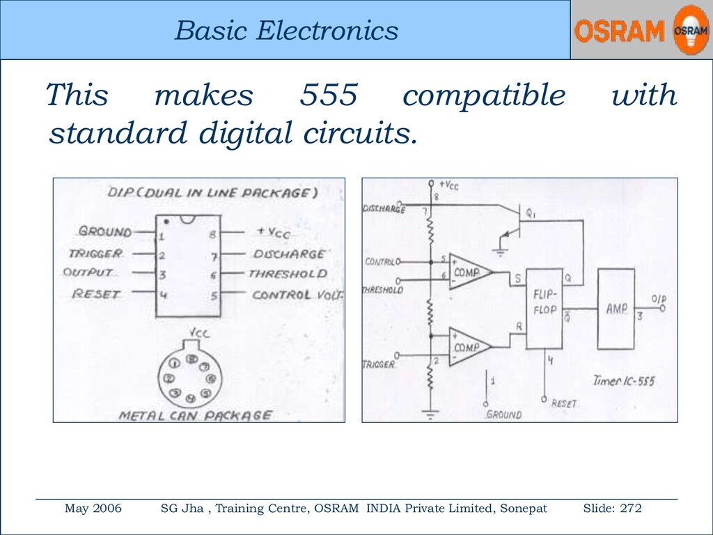
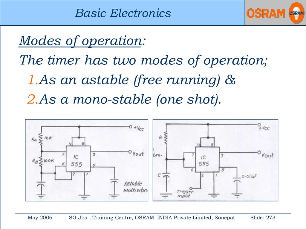
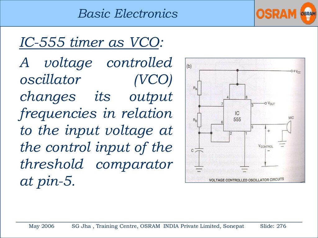
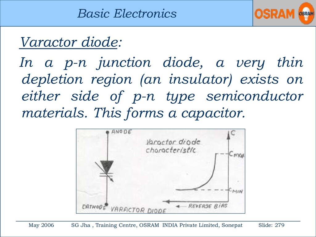
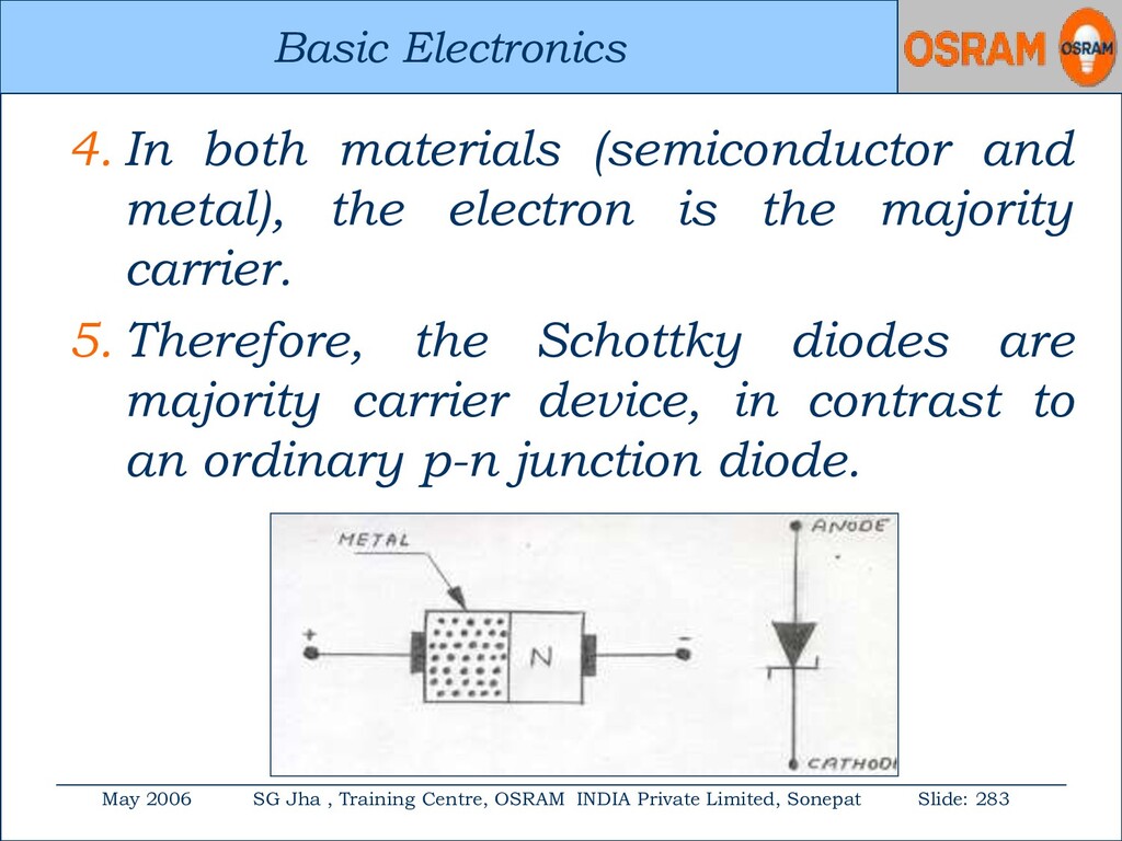
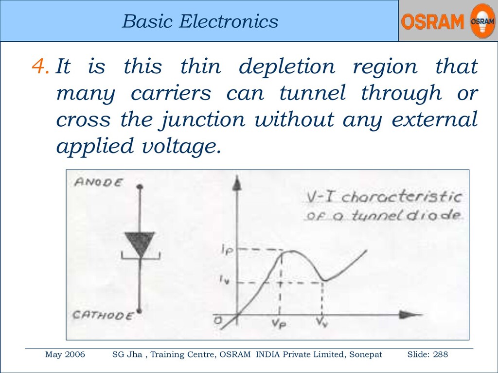
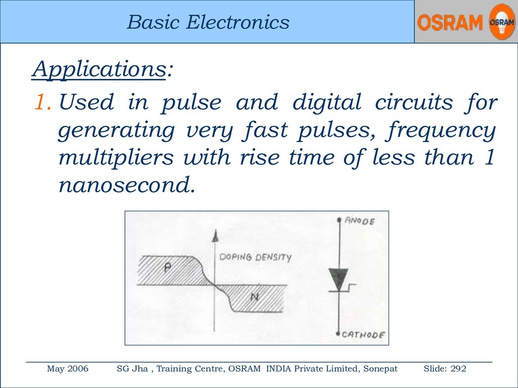
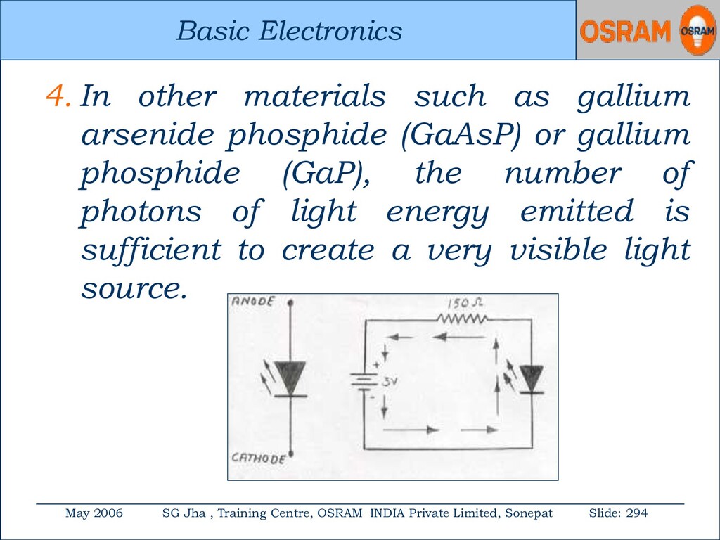
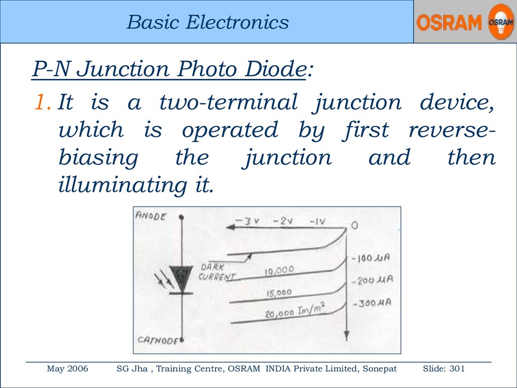
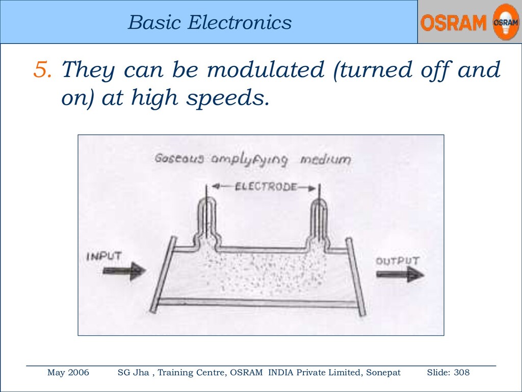
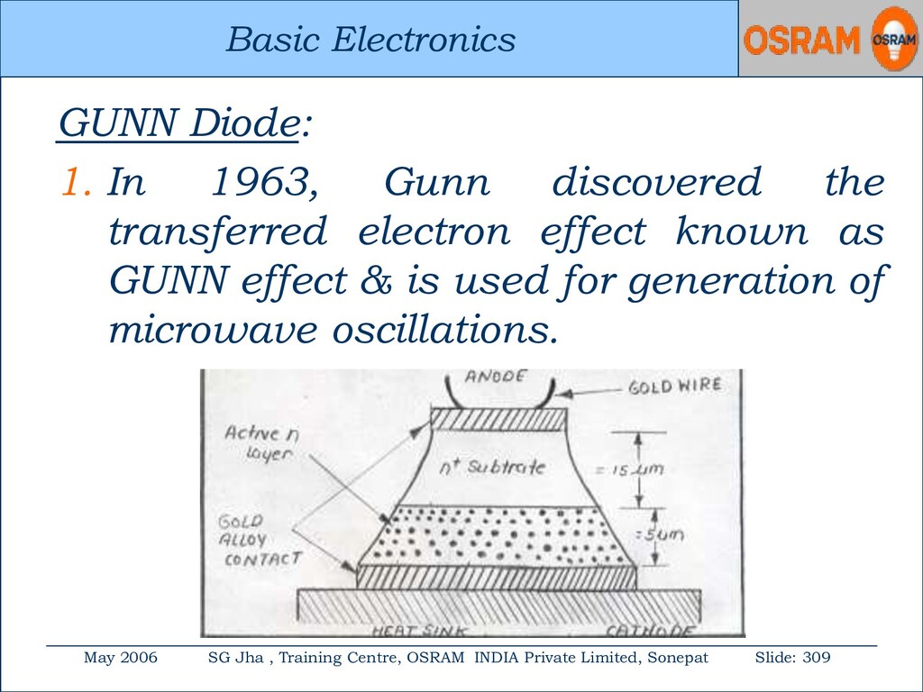
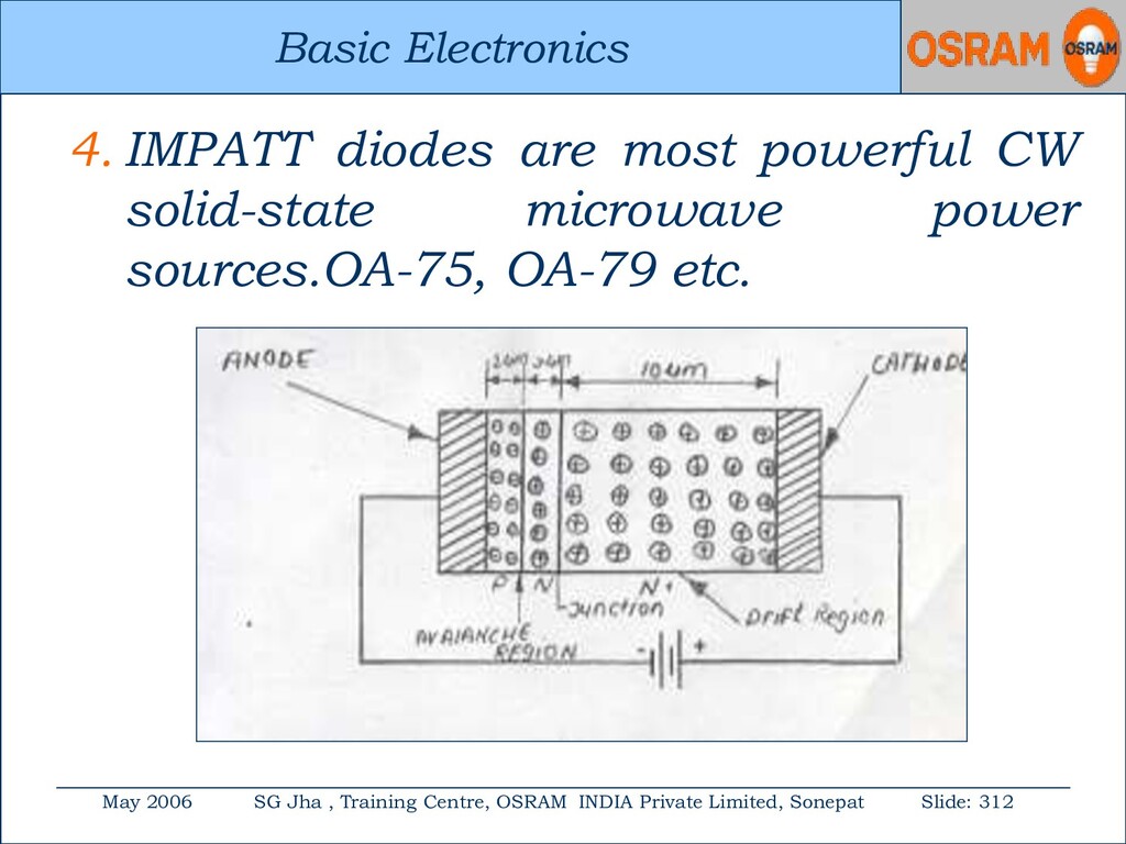
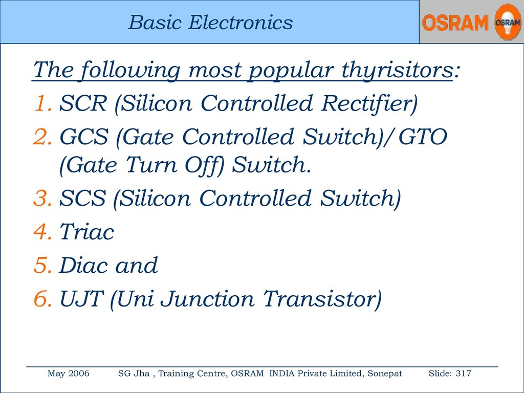
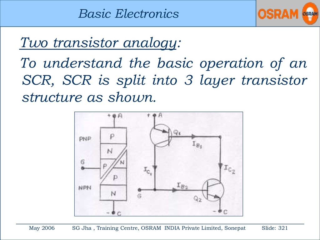
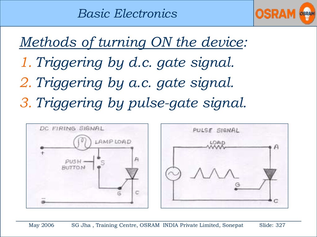
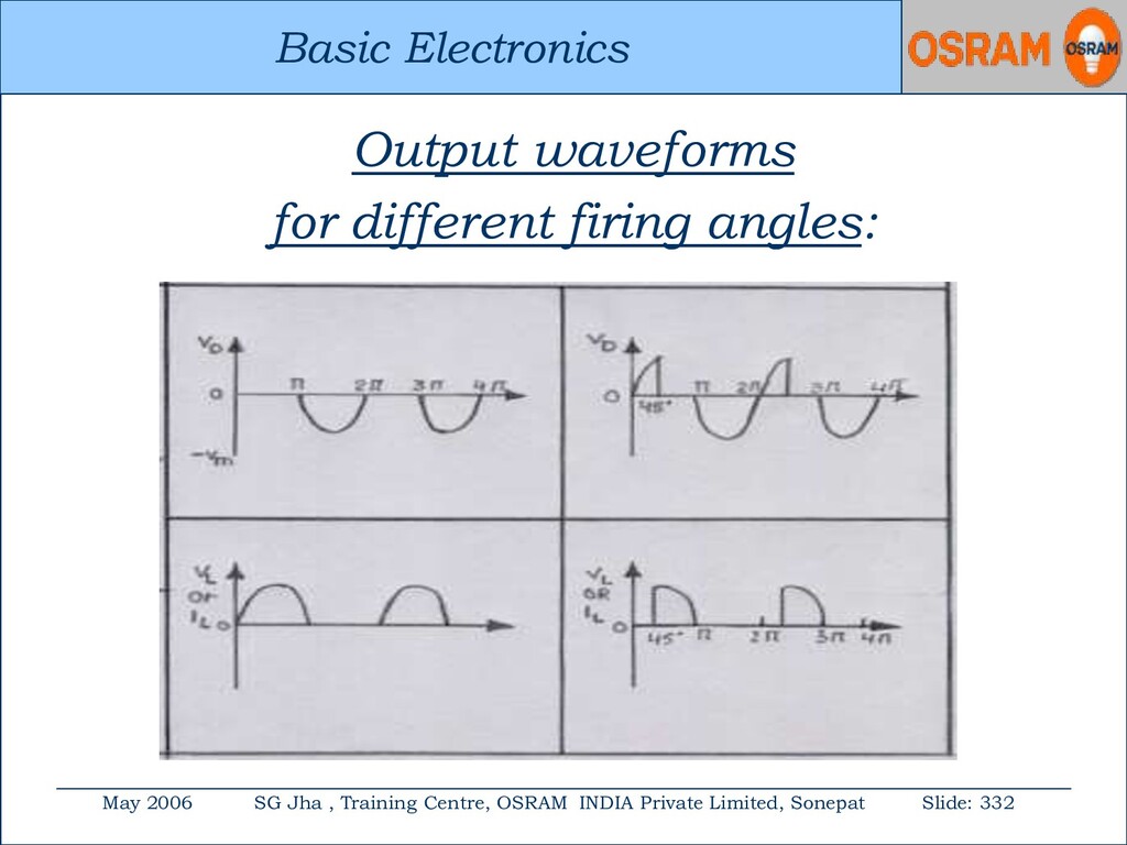
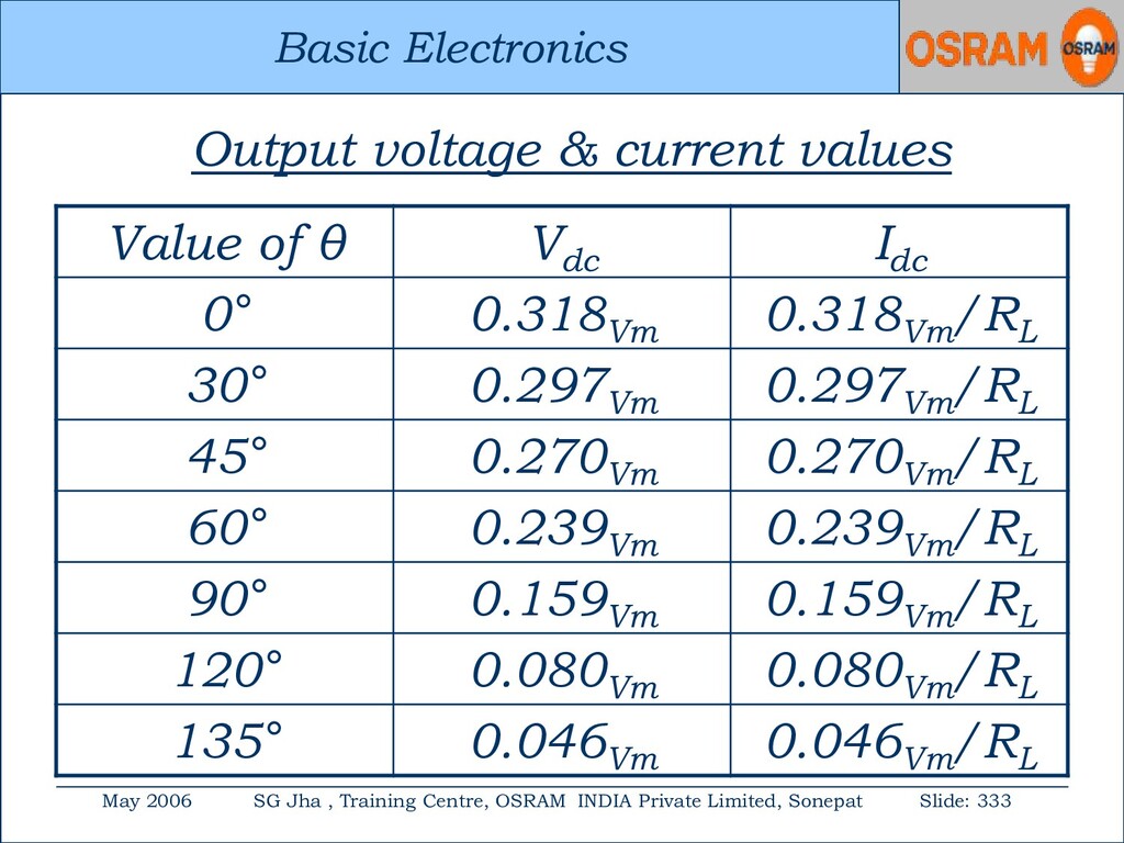
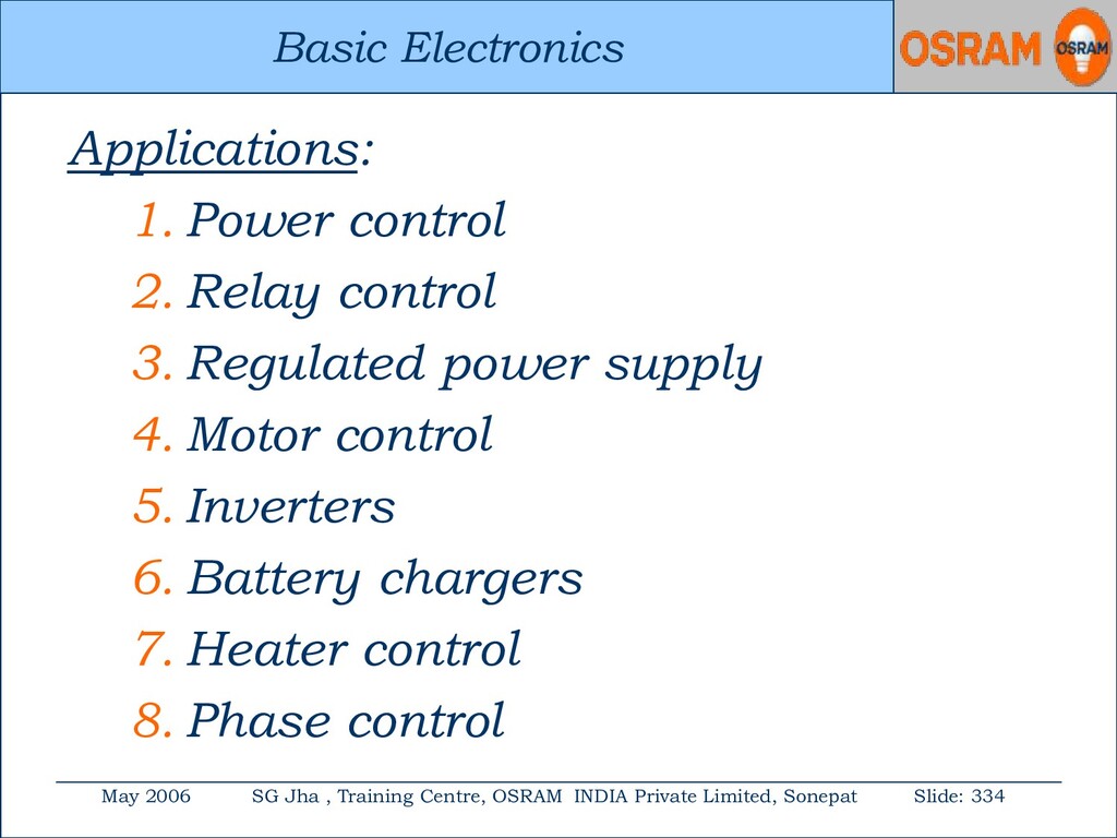
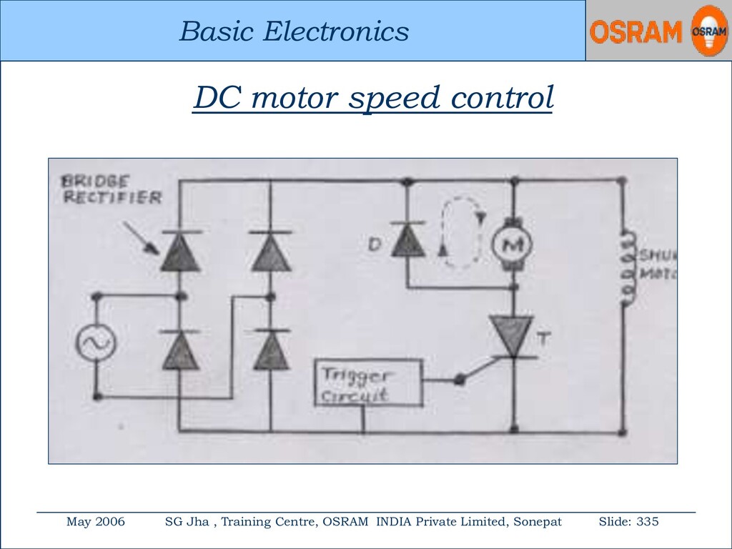
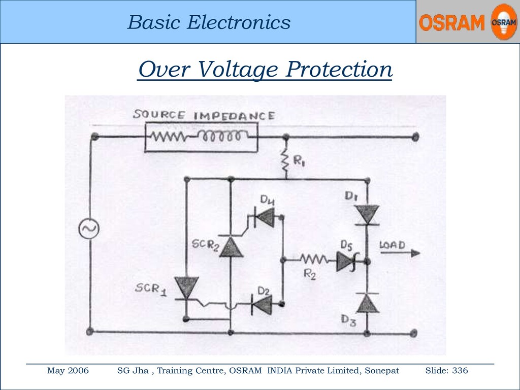
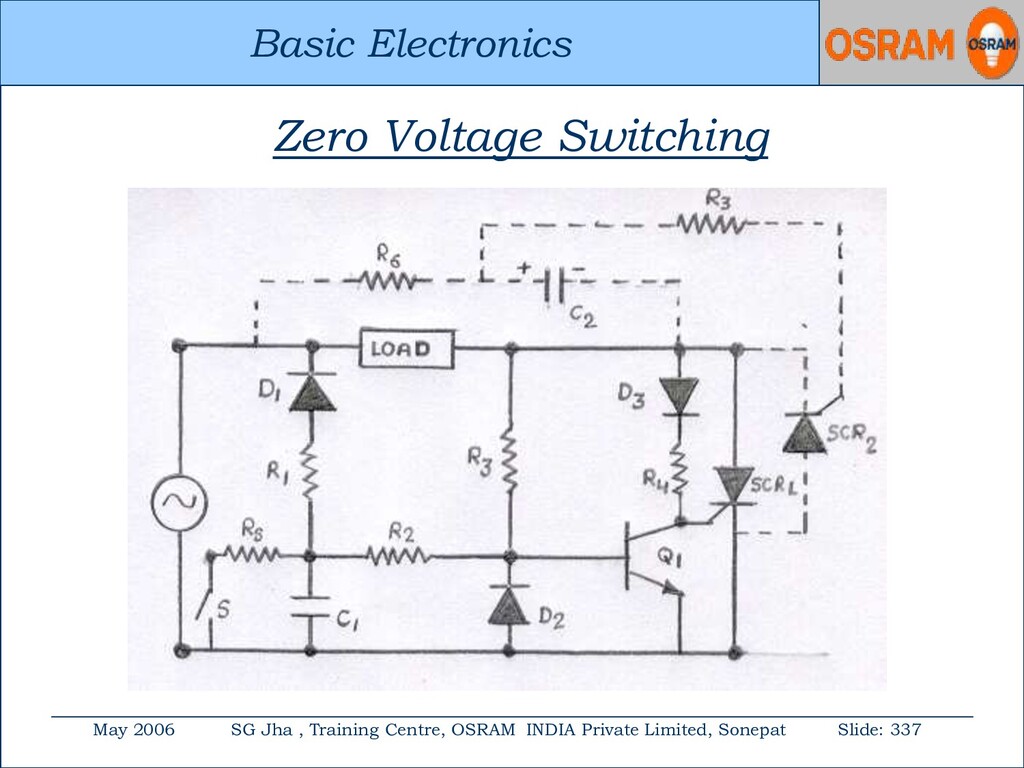
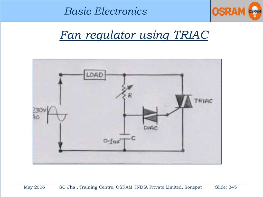
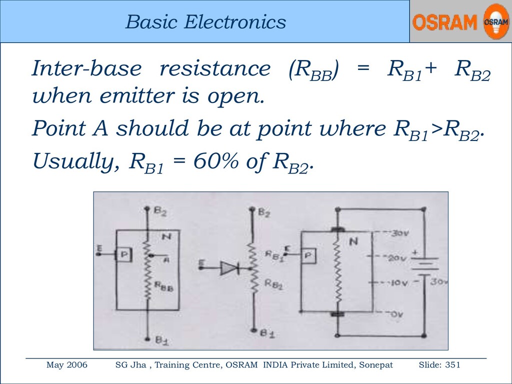
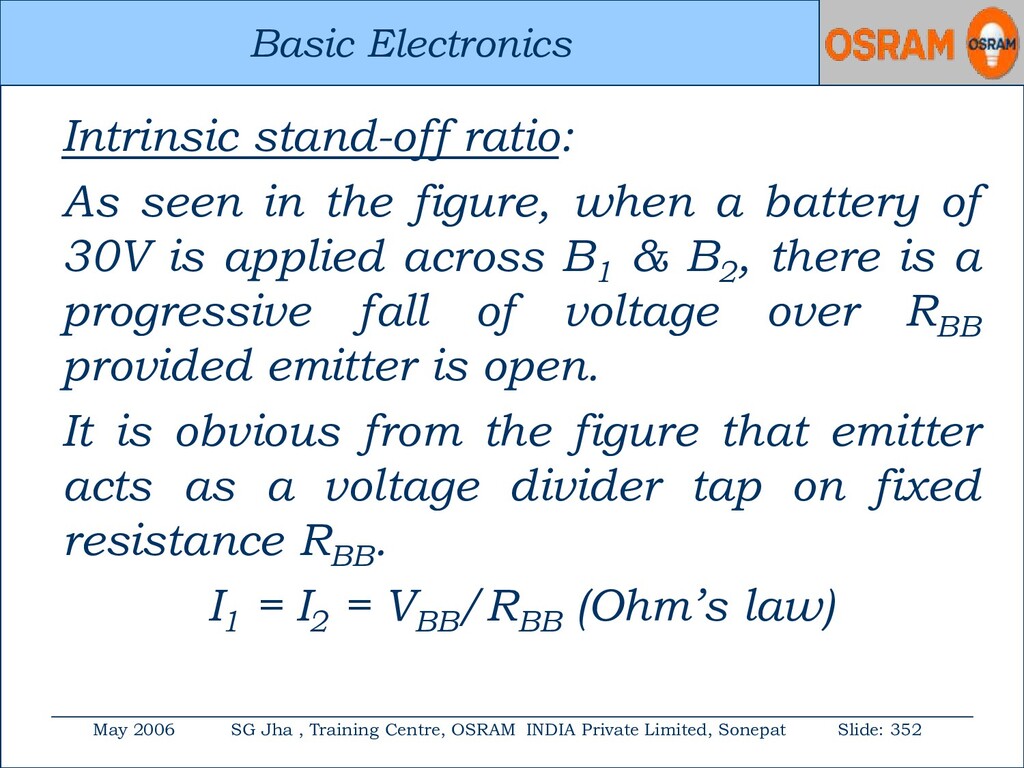
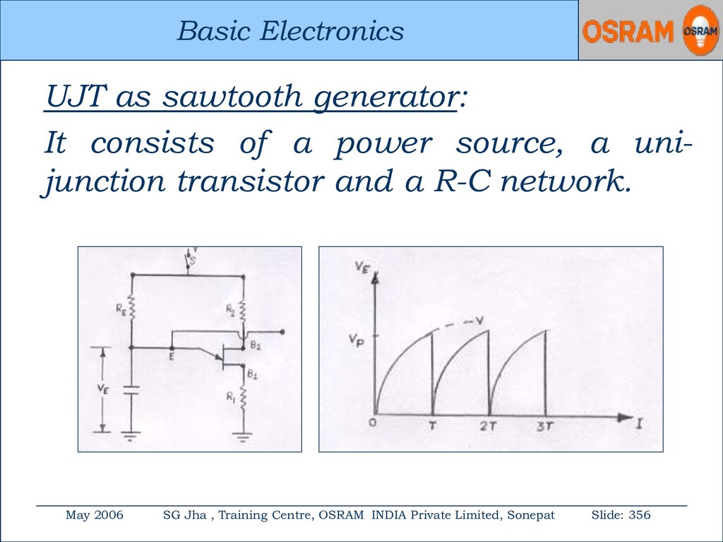
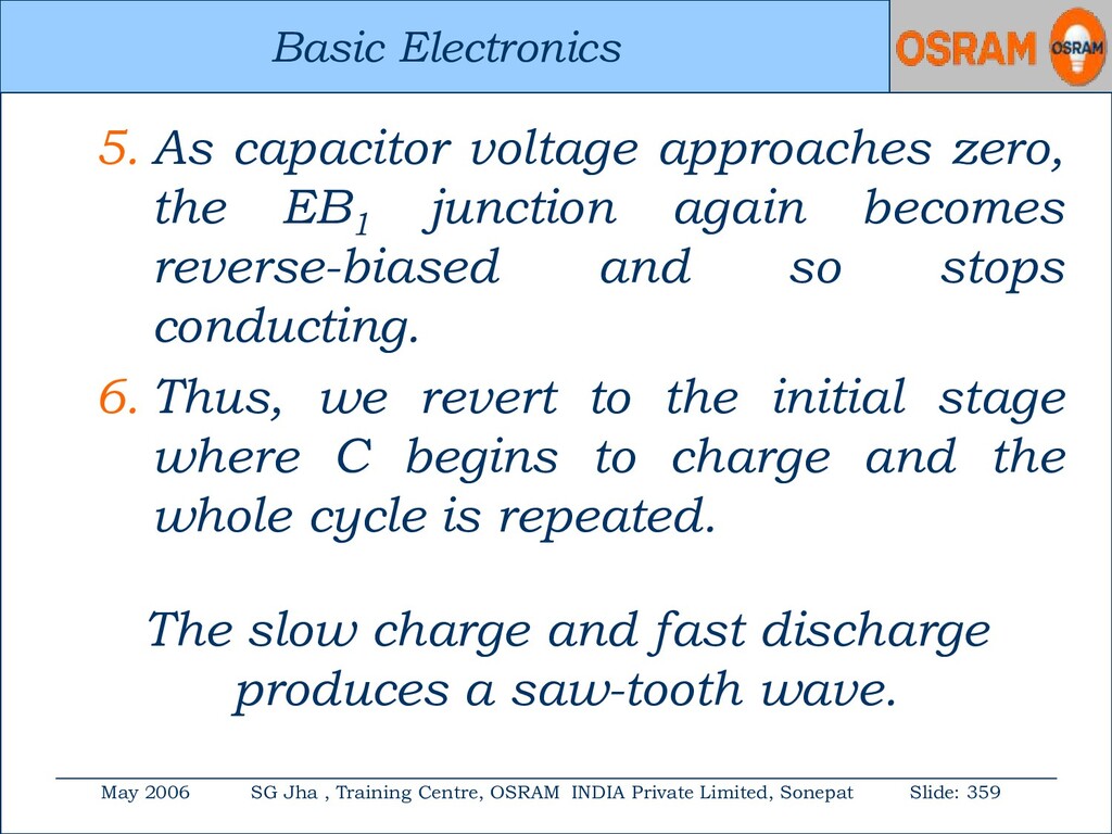
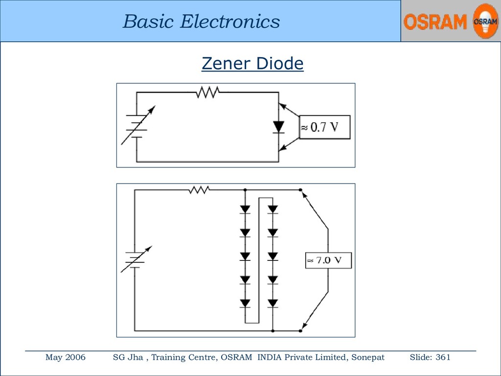
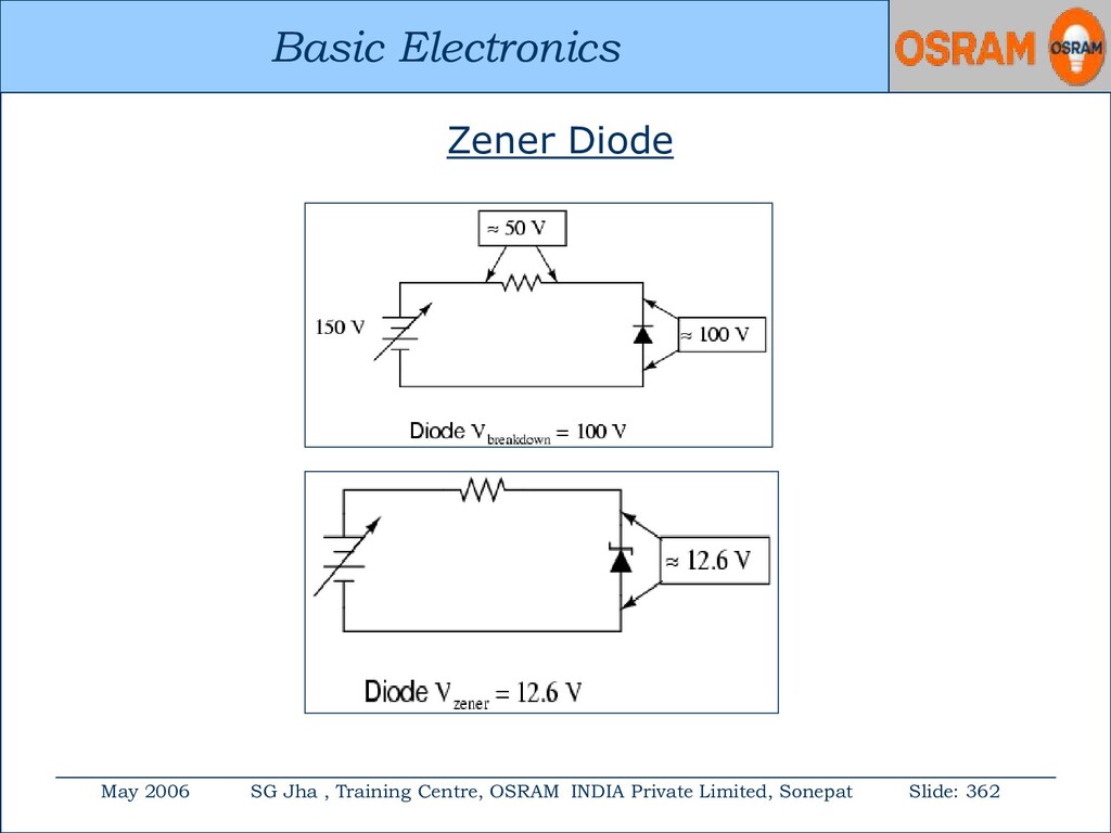
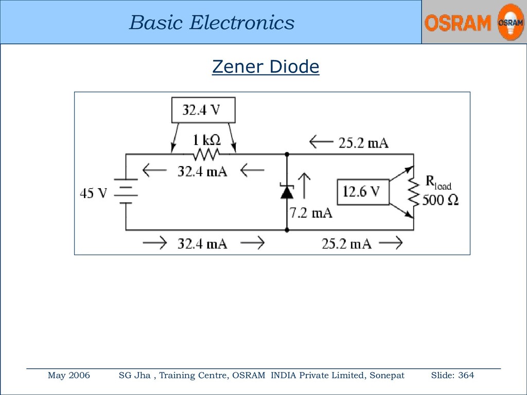
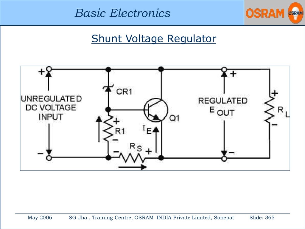
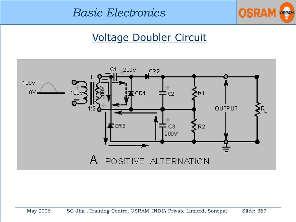
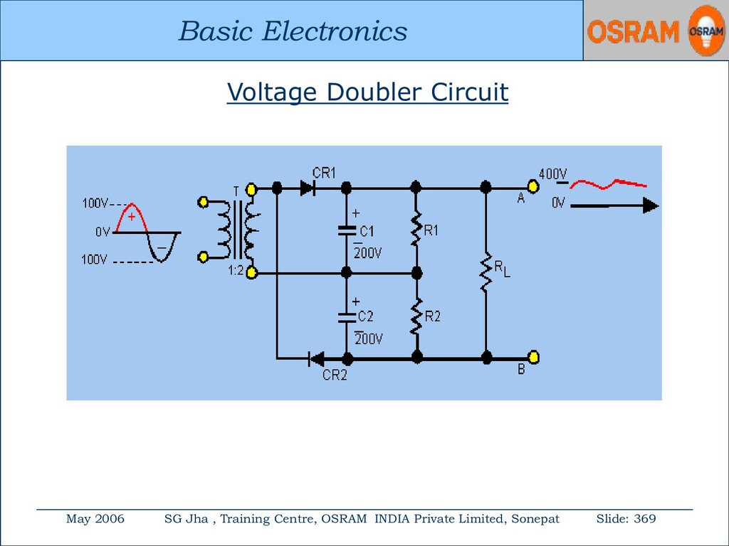
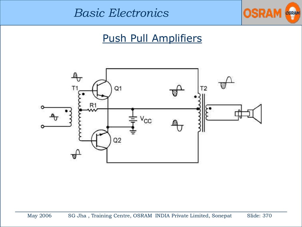