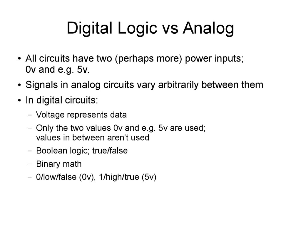
more) power inputs; 0v and e.g. 5v. • Signals in analog circuits vary arbitrarily between them • In digital circuits: – Voltage represents data – Only the two values 0v and e.g. 5v are used; values in between aren't used – Boolean logic; true/false – Binary math – 0/low/false (0v), 1/high/true (5v)
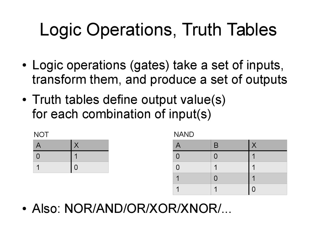
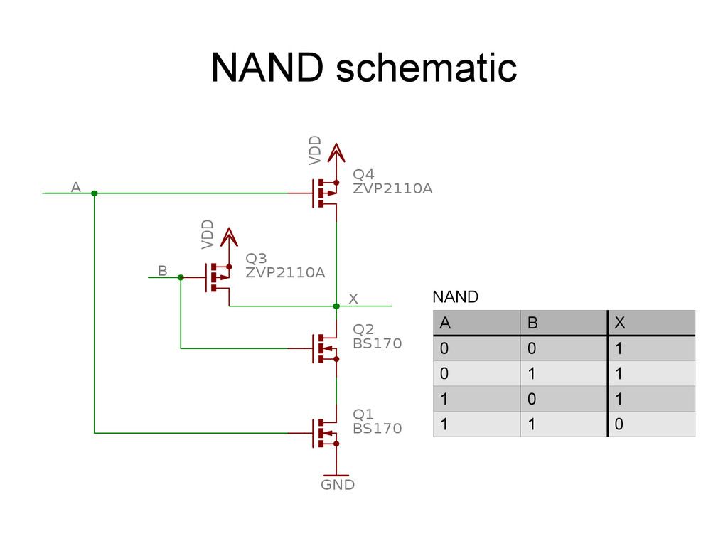
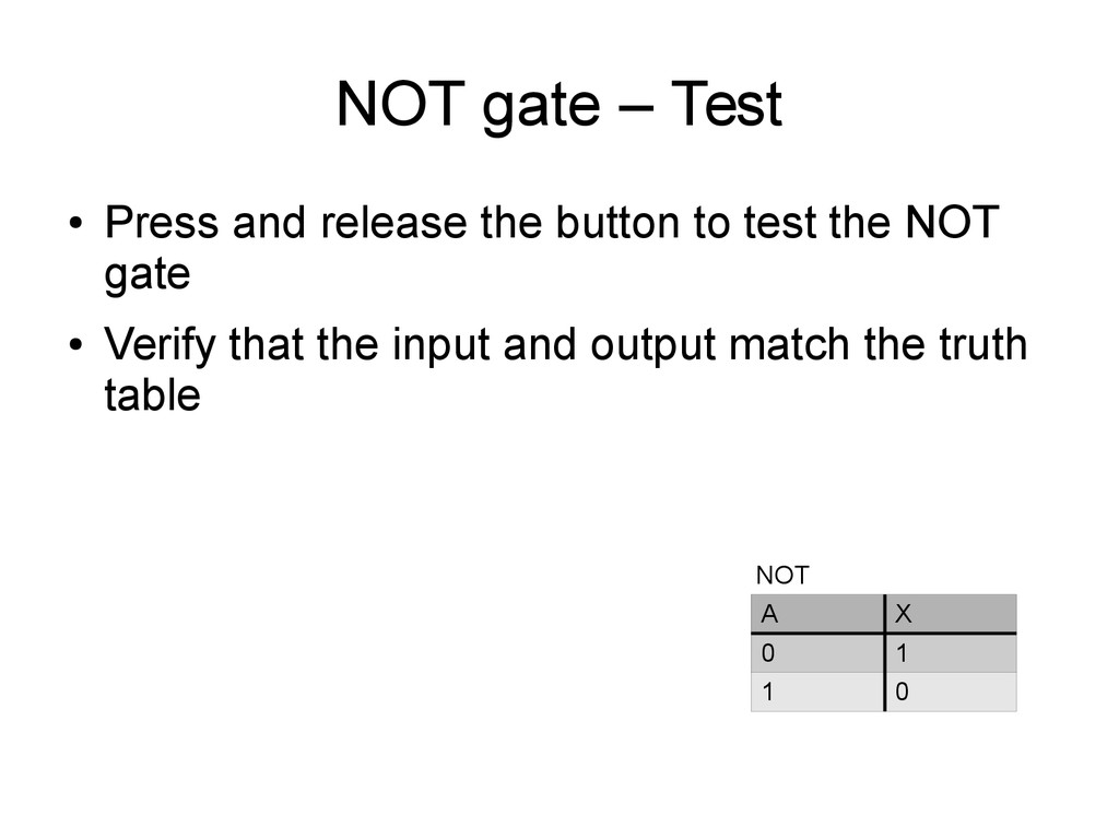
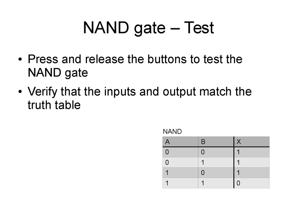
• Logic operations (gates) take a set of inputs, transform them, and produce a set of outputs • Truth tables define output value(s) for each combination of input(s) • Also: NOR/AND/OR/XOR/XNOR/... NOT A B X 0 0 1 0 1 1 1 0 1 1 1 0 NAND
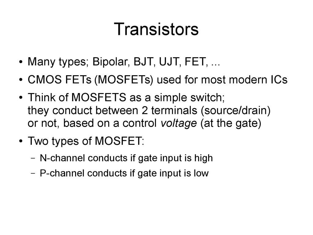
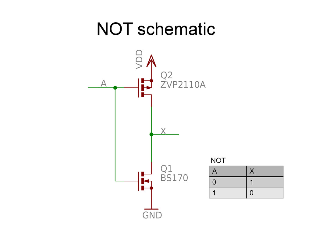
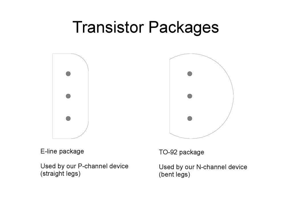
CMOS FETs (MOSFETs) used for most modern ICs • Think of MOSFETS as a simple switch; they conduct between 2 terminals (source/drain) or not, based on a control voltage (at the gate) • Two types of MOSFET: – N-channel conducts if gate input is high – P-channel conducts if gate input is low
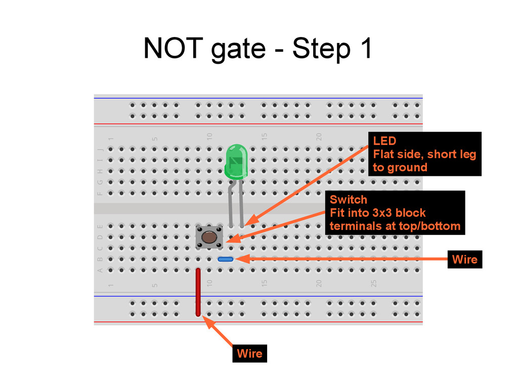
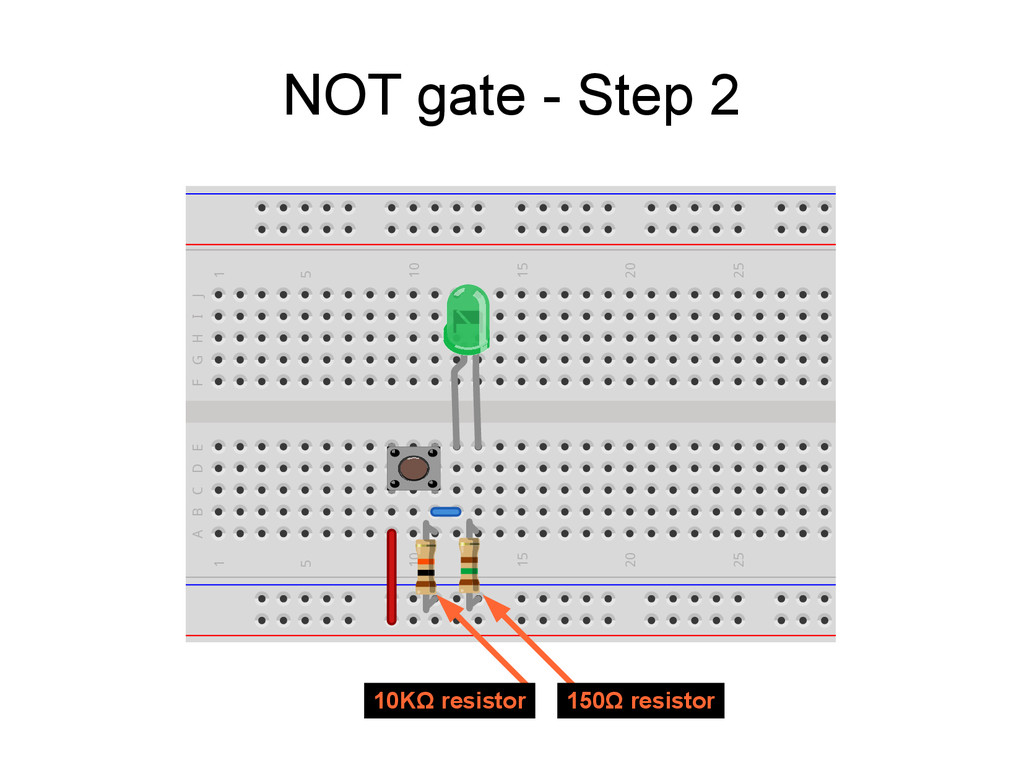
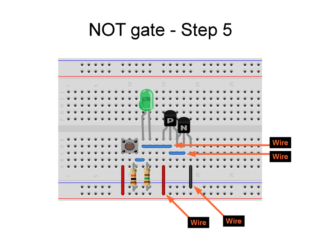
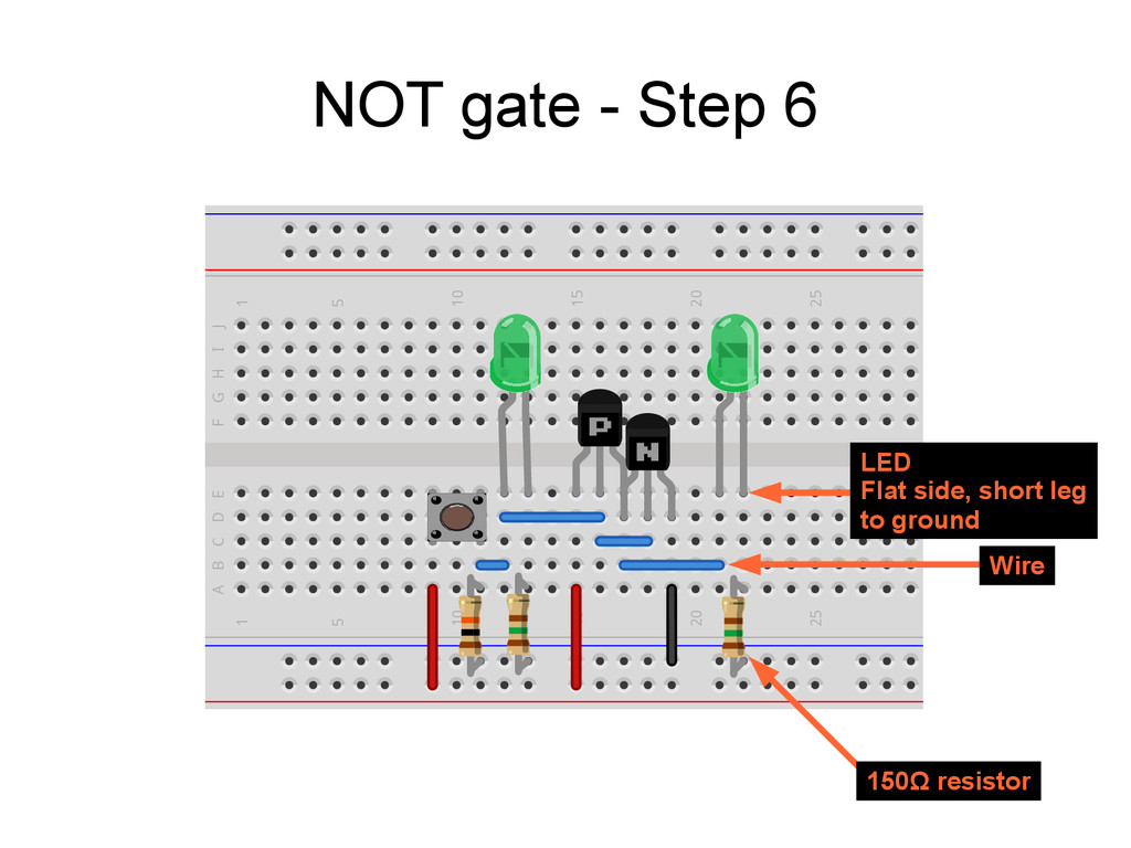
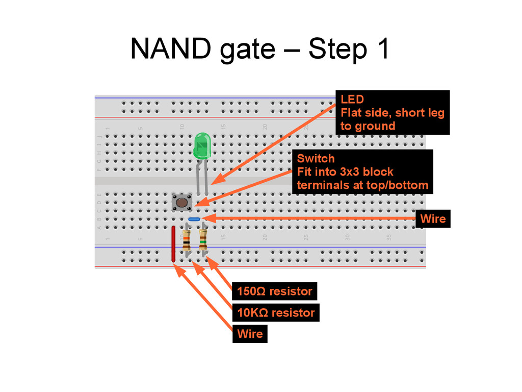
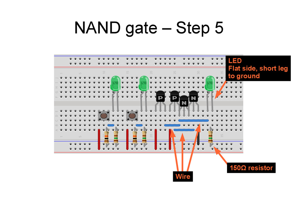
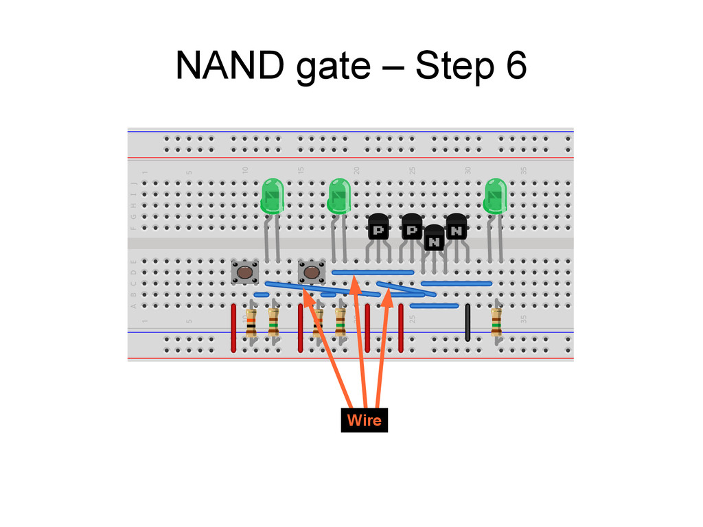
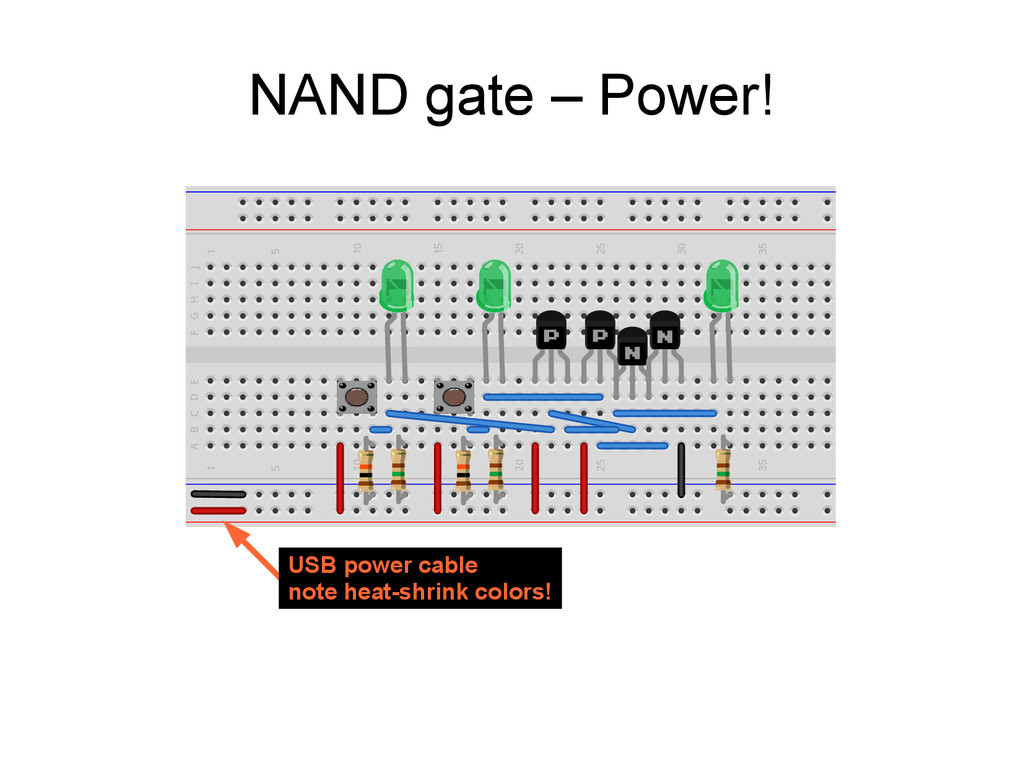
10 15 15 20 20 25 25 30 30 35 35 40 40 45 45 50 50 A B C D E F G H I J LED Flat side, short leg to ground Switch Fit into 3x3 block terminals at top/bottom Wire Wire 150Ω resistor 10KΩ resistor
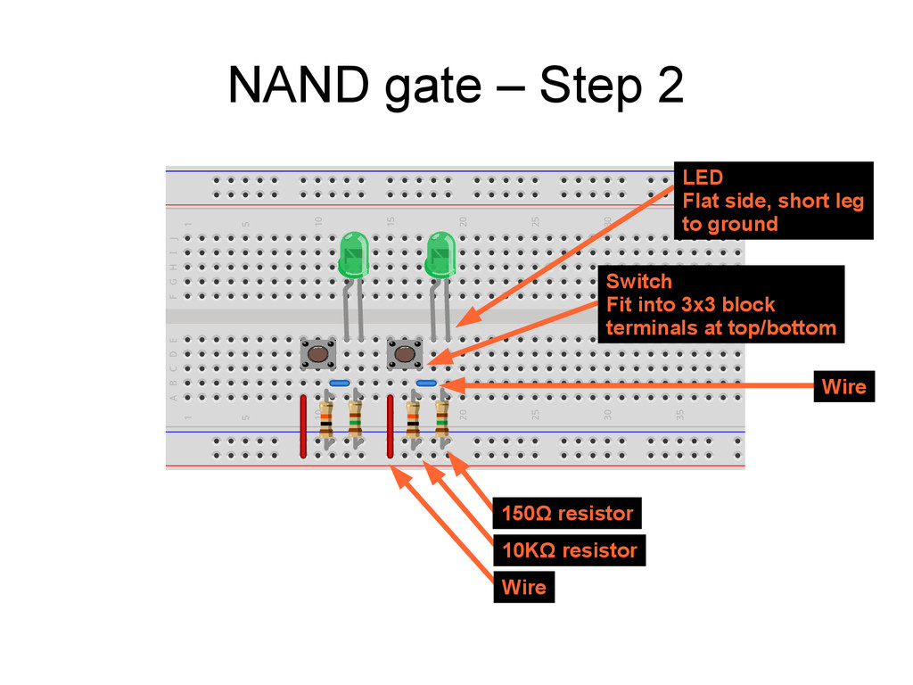
10 15 15 20 20 25 25 30 30 35 35 40 40 45 45 50 50 A B C D E F G H I J LED Flat side, short leg to ground Switch Fit into 3x3 block terminals at top/bottom Wire Wire 150Ω resistor 10KΩ resistor
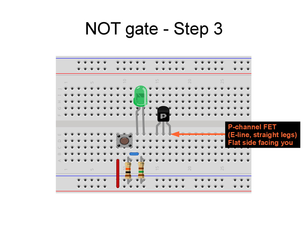
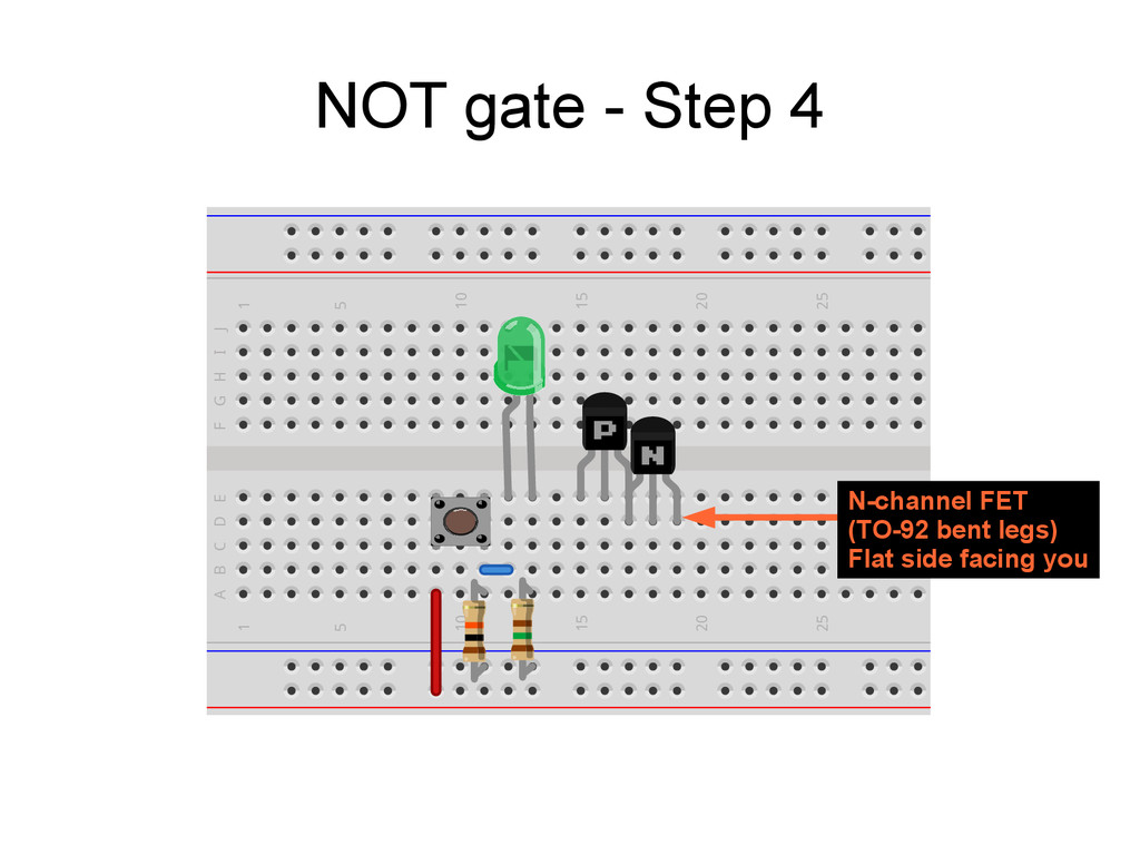
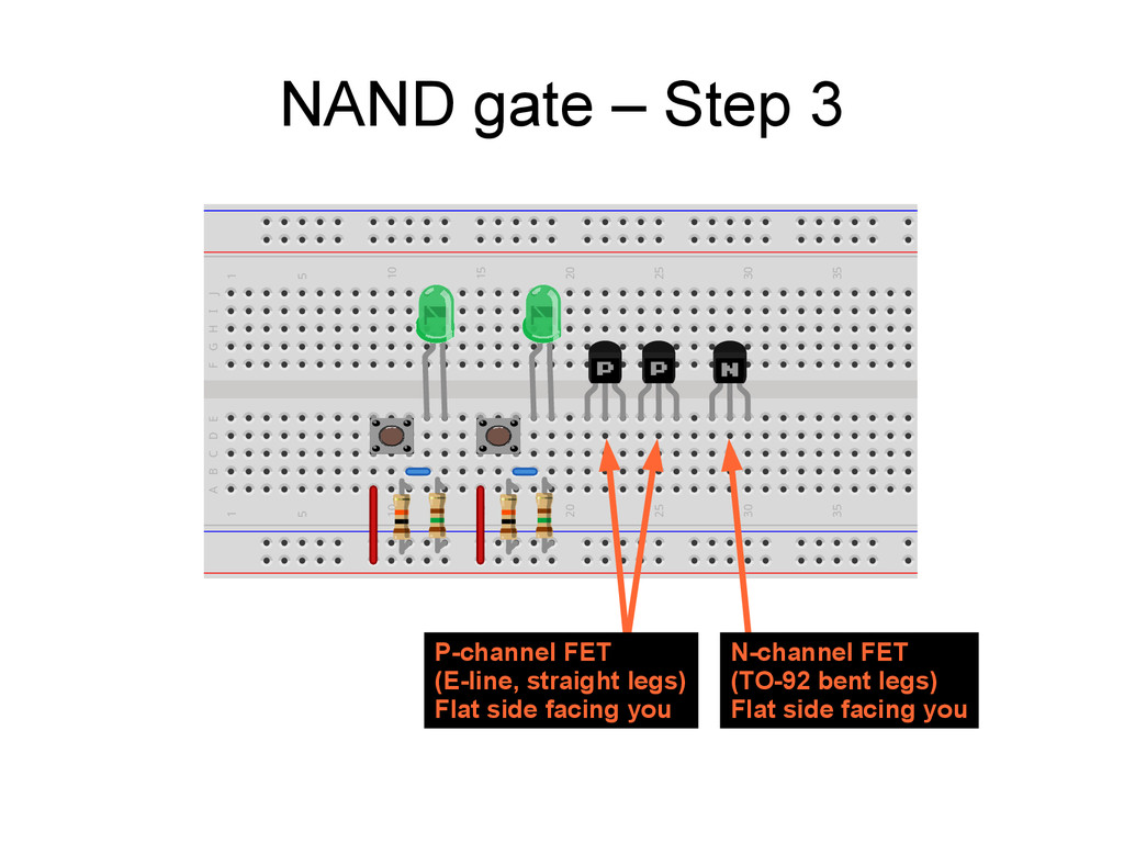
25 25 30 30 35 35 40 40 45 45 50 50 A B C D E F G H I J NAND gate – Step 3 P-channel FET (E-line, straight legs) Flat side facing you N-channel FET (TO-92 bent legs) Flat side facing you