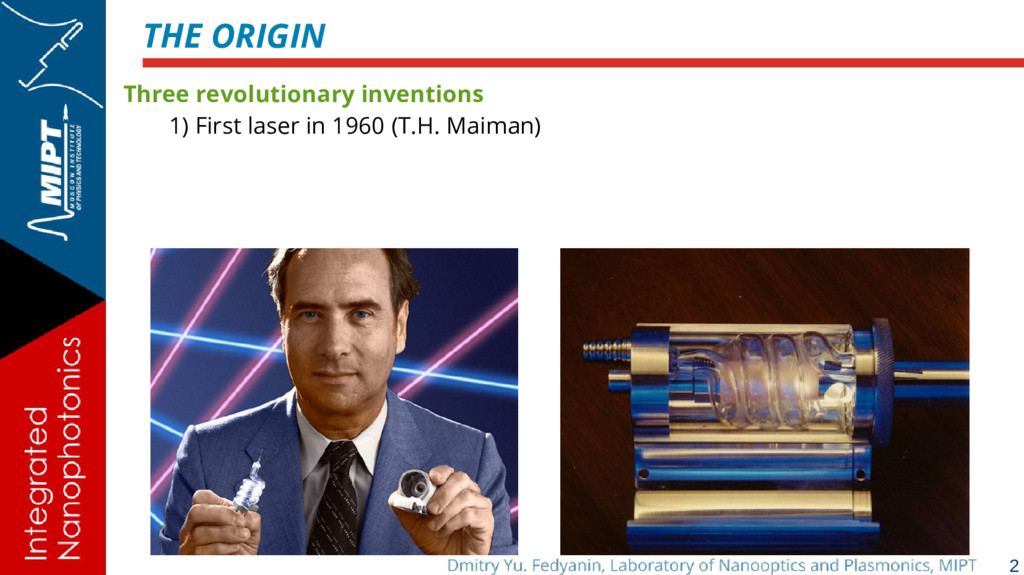
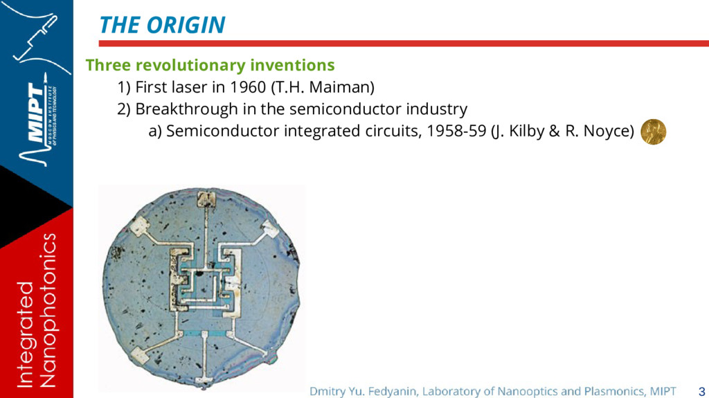
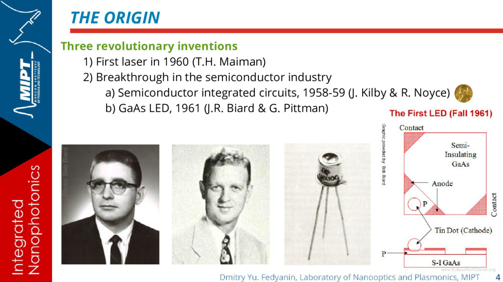
1960 (T.H. Maiman) 2) Breakthrough in the semiconductor industry a) Semiconductor integrated circuits, 1958-59 (J. Kilby & R. Noyce) b) GaAs LED, 1961 (J.R. Biard & G. Pittman)
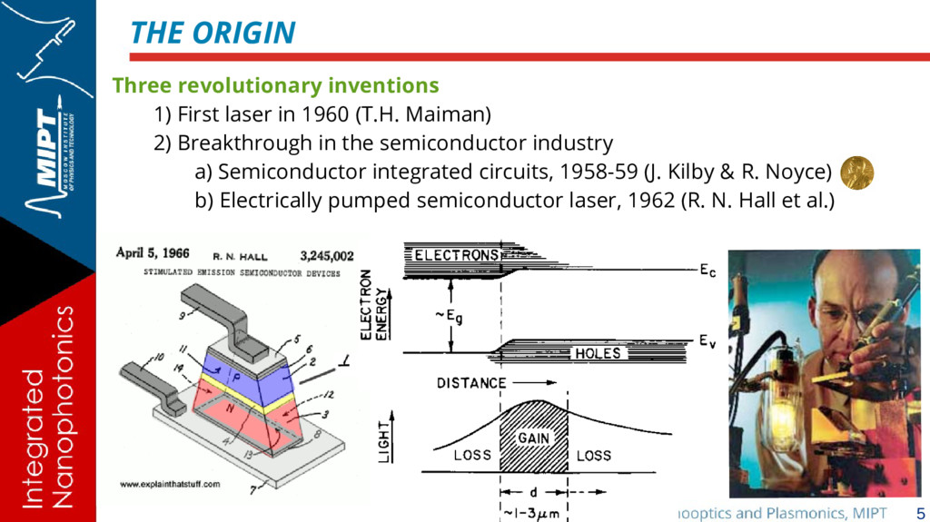
1960 (T.H. Maiman) 2) Breakthrough in the semiconductor industry a) Semiconductor integrated circuits, 1958-59 (J. Kilby & R. Noyce) b) Electrically pumped semiconductor laser, 1962 (R. N. Hall et al.)
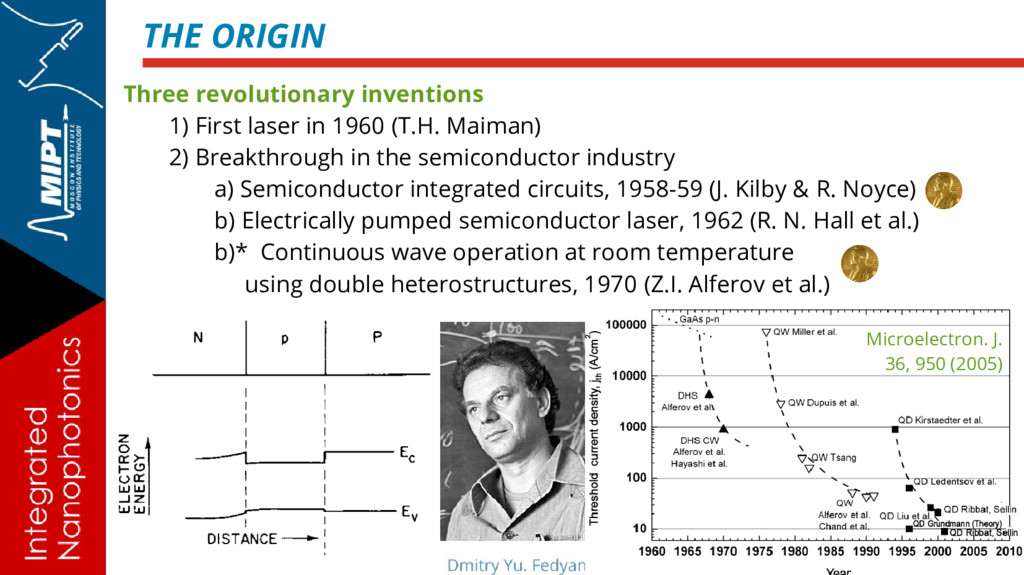
1960 (T.H. Maiman) 2) Breakthrough in the semiconductor industry a) Semiconductor integrated circuits, 1958-59 (J. Kilby & R. Noyce) b) Electrically pumped semiconductor laser, 1962 (R. N. Hall et al.) b)* Continuous wave operation at room temperature using double heterostructures, 1970 (Z.I. Alferov et al.) Microelectron. J. 36, 950 (2005)
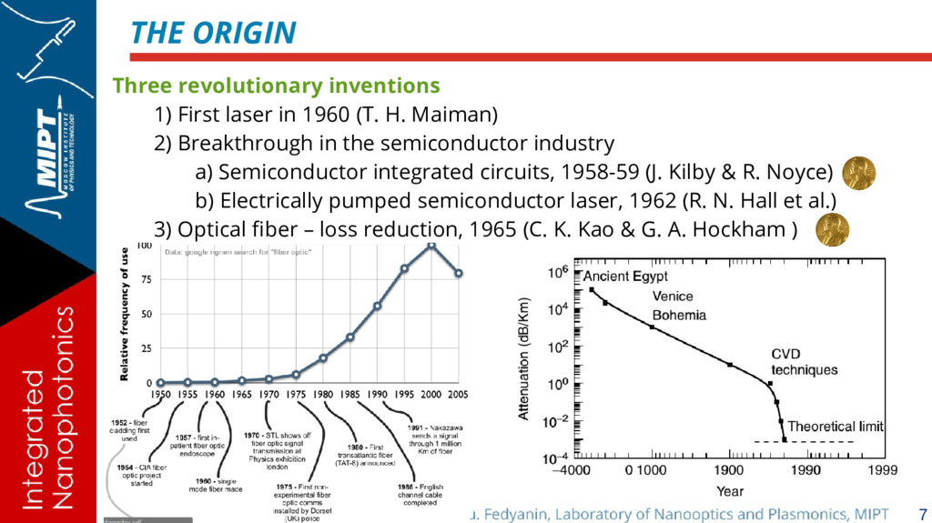
1960 (T. H. Maiman) 2) Breakthrough in the semiconductor industry a) Semiconductor integrated circuits, 1958-59 (J. Kilby & R. Noyce) b) Electrically pumped semiconductor laser, 1962 (R. N. Hall et al.) 3) Optical fiber – loss reduction, 1965 (C. K. Kao & G. A. Hockham )
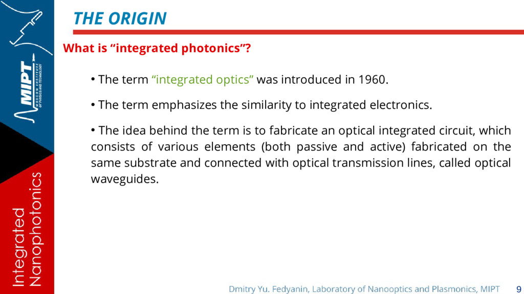
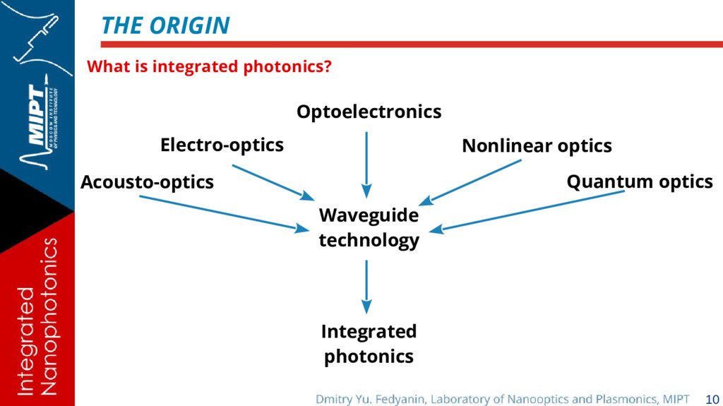
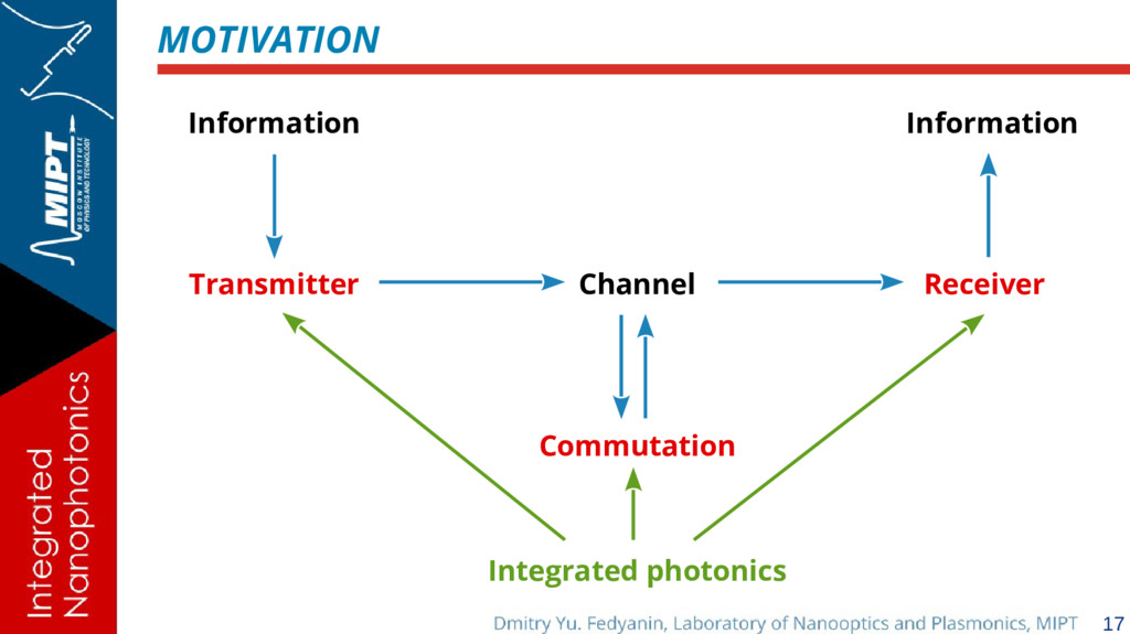
“integrated optics” was introduced in 1960. • The term emphasizes the similarity to integrated electronics. • The idea behind the term is to fabricate an optical integrated circuit, which consists of various elements (both passive and active) fabricated on the same substrate and connected with optical transmission lines, called optical waveguides.
can give the maximum bandwidth of up to 194x1012 Hz! 1% of this value is 2 THz, which is roughly equal to a bit rate of 2 Tbit/s. 2 THz = 4x10⁵ analog video channels at a bandwidth of 5 MHz = 4x10⁸ telephone calls at 5 kHz per call
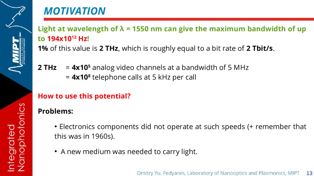
can give the maximum bandwidth of up to 194x1012 Hz! 1% of this value is 2 THz, which is roughly equal to a bit rate of 2 Tbit/s. 2 THz = 4x10⁵ analog video channels at a bandwidth of 5 MHz = 4x10⁸ telephone calls at 5 kHz per call How to use this potential? Problems: • Electronics components did not operate at such speeds (+ remember that this was in 1960s). • A new medium was needed to carry light.
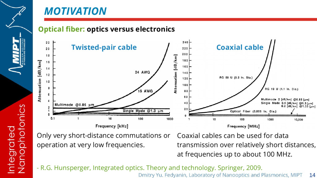
cable - R.G. Hunsperger, Integrated optics. Theory and technology. Springer, 2009. Only very short-distance commutations or operation at very low frequencies. Coaxial cables can be used for data transmission over relatively short distances, at frequencies up to about 100 MHz.
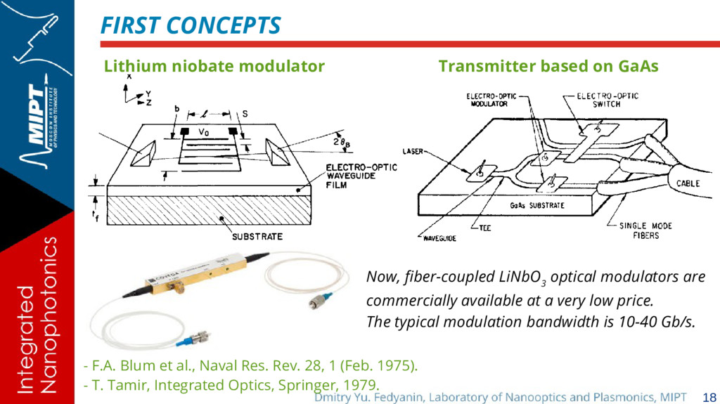
et al., Naval Res. Rev. 28, 1 (Feb. 1975). - T. Tamir, Integrated Optics, Springer, 1979. Lithium niobate modulator Now, fiber-coupled LiNbO 3 optical modulators are commercially available at a very low price. The typical modulation bandwidth is 10-40 Gb/s.
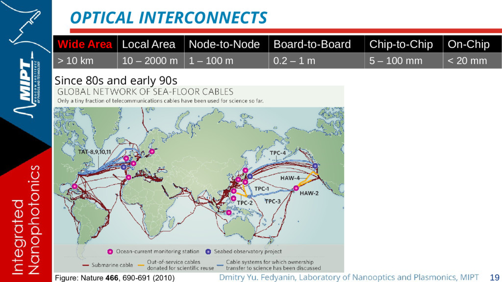
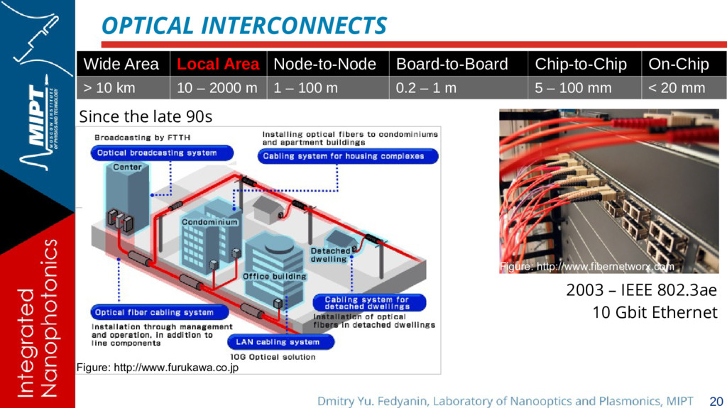
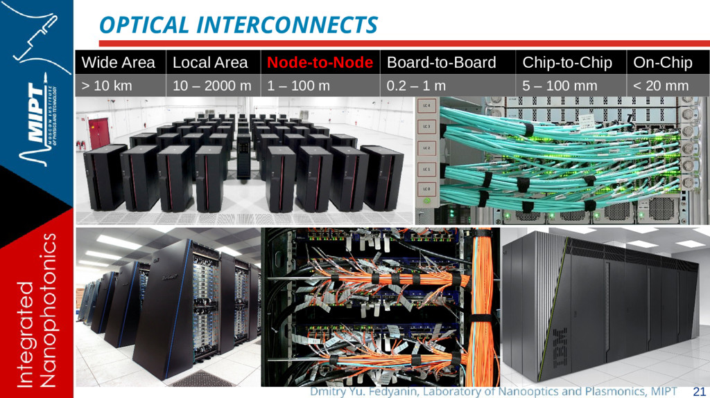
On-Chip > 10 km 10 – 2000 m 1 – 100 m 0.2 – 1 m 5 – 100 mm < 20 mm Since the late 90s Figure: http://www.furukawa.co.jp Figure: http://www.fibernetworx.com 2003 – IEEE 802.3ae 10 Gbit Ethernet
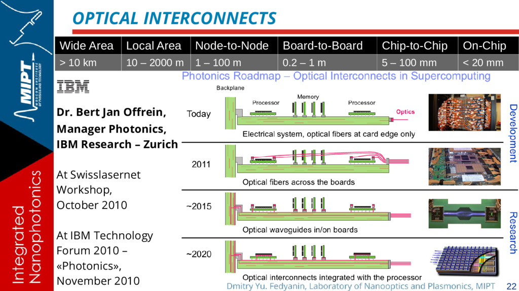
On-Chip > 10 km 10 – 2000 m 1 – 100 m 0.2 – 1 m 5 – 100 mm < 20 mm Dr. Bert Jan Offrein, Manager Photonics, IBM Research – Zurich At Swisslasernet Workshop, October 2010 At IBM Technology Forum 2010 – «Photonics», November 2010
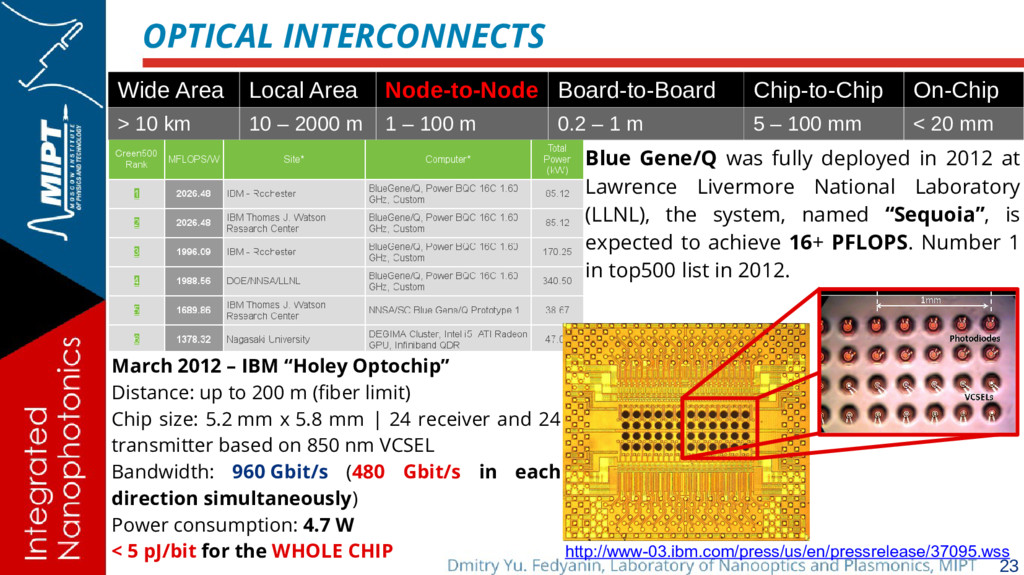
On-Chip > 10 km 10 – 2000 m 1 – 100 m 0.2 – 1 m 5 – 100 mm < 20 mm March 2012 – IBM “Holey Optochip” Distance: up to 200 m (fiber limit) Chip size: 5.2 mm x 5.8 mm | 24 receiver and 24 transmitter based on 850 nm VCSEL Bandwidth: 960 Gbit/s (480 Gbit/s in each direction simultaneously) Power consumption: 4.7 W < 5 pJ/bit for the WHOLE CHIP http://www-03.ibm.com/press/us/en/pressrelease/37095.wss Blue Gene/Q was fully deployed in 2012 at Lawrence Livermore National Laboratory (LLNL), the system, named “Sequoia”, is expected to achieve 16+ PFLOPS. Number 1 in top500 list in 2012.
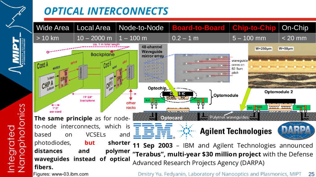
On-Chip > 10 km 10 – 2000 m 1 – 100 m 0.2 – 1 m 5 – 100 mm < 20 mm Figures: www-03.ibm.com 11 Sep 2003 – IBM and Agilent Technologies announced “Terabus”, multi-year $30 million project with the Defense Advanced Research Projects Agency (DARPA) The same principle as for node- to-node interconnects, which is based on VCSELs and photodiodes, but shorter distances and polymer waveguides instead of optical fibers.
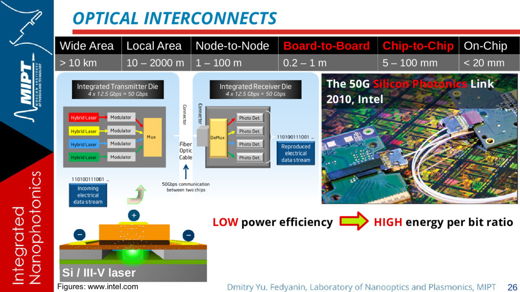
On-Chip > 10 km 10 – 2000 m 1 – 100 m 0.2 – 1 m 5 – 100 mm < 20 mm Figures: www.intel.com The 50G Silicon Photonics Link 2010, Intel Si / III-V laser LOW power efficiency HIGH energy per bit ratio
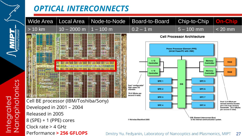
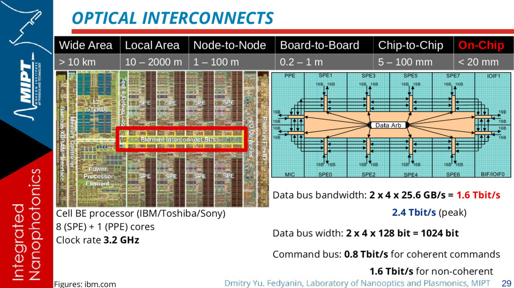
On-Chip > 10 km 10 – 2000 m 1 – 100 m 0.2 – 1 m 5 – 100 mm < 20 mm Cell BE processor (IBM/Toshiba/Sony) Developed in 2001 – 2004 Released in 2005 8 (SPE) + 1 (PPE) cores Clock rate > 4 GHz Performance > 256 GFLOPS Figure: ibm.com
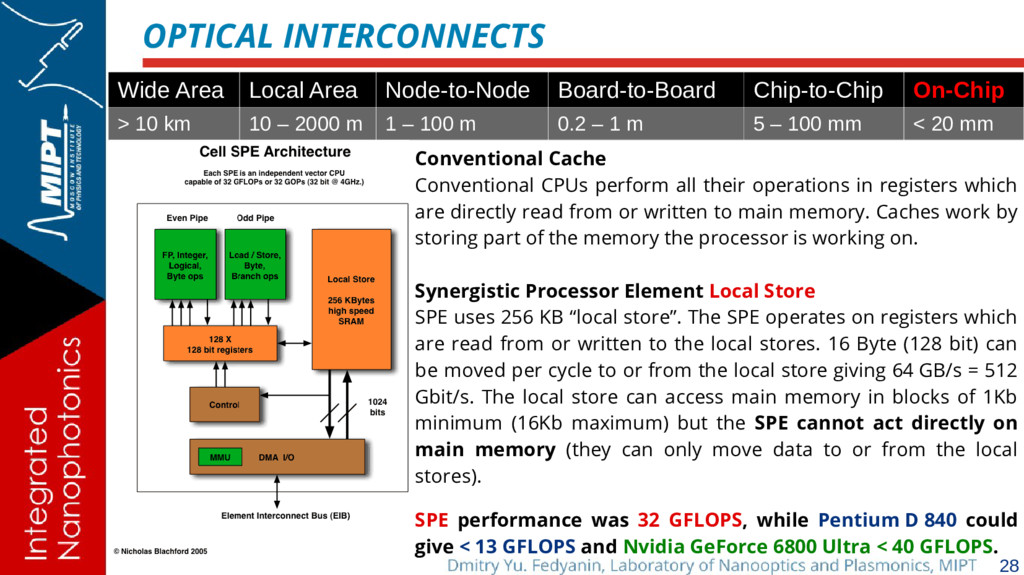
On-Chip > 10 km 10 – 2000 m 1 – 100 m 0.2 – 1 m 5 – 100 mm < 20 mm Conventional Cache Conventional CPUs perform all their operations in registers which are directly read from or written to main memory. Caches work by storing part of the memory the processor is working on. Synergistic Processor Element Local Store SPE uses 256 KB “local store”. The SPE operates on registers which are read from or written to the local stores. 16 Byte (128 bit) can be moved per cycle to or from the local store giving 64 GB/s = 512 Gbit/s. The local store can access main memory in blocks of 1Kb minimum (16Kb maximum) but the SPE cannot act directly on main memory (they can only move data to or from the local stores). SPE performance was 32 GFLOPS, while Pentium D 840 could give < 13 GFLOPS and Nvidia GeForce 6800 Ultra < 40 GFLOPS.
On-Chip > 10 km 10 – 2000 m 1 – 100 m 0.2 – 1 m 5 – 100 mm < 20 mm Cell BE processor (IBM/Toshiba/Sony) 8 (SPE) + 1 (PPE) cores Clock rate 3.2 GHz Data bus bandwidth: 2 x 4 x 25.6 GB/s = 1.6 Tbit/s 2.4 Tbit/s (peak) Data bus width: 2 x 4 x 128 bit = 1024 bit Command bus: 0.8 Tbit/s for coherent commands 1.6 Tbit/s for non-coherent Figures: ibm.com
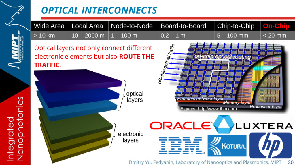
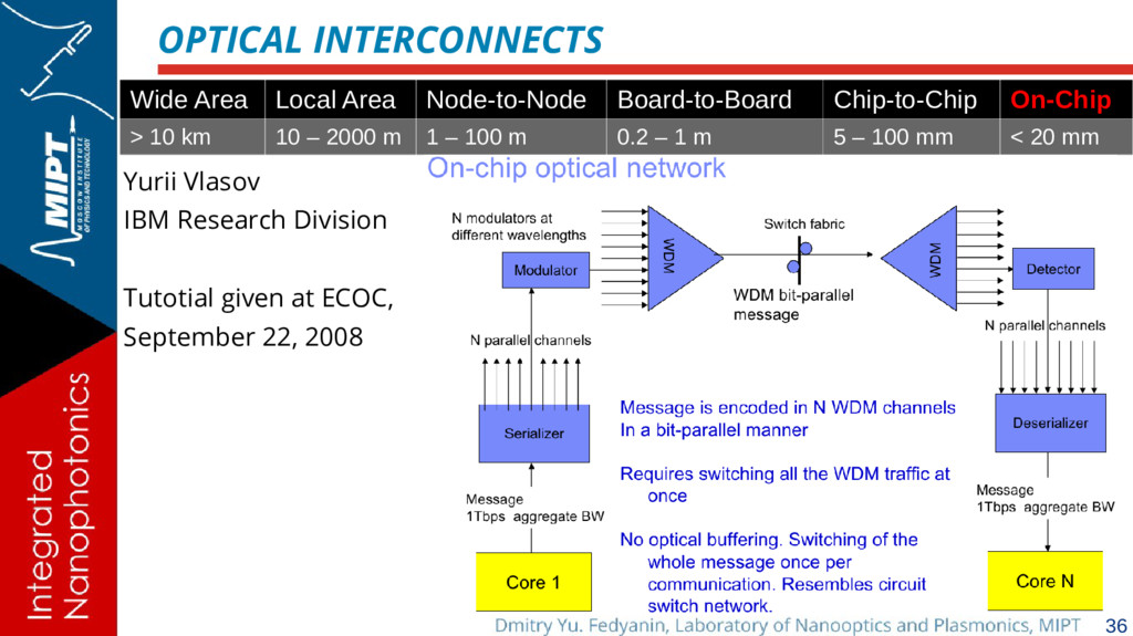
On-Chip > 10 km 10 – 2000 m 1 – 100 m 0.2 – 1 m 5 – 100 mm < 20 mm Figures: http://www.ibm.com Optical layers not only connect different electronic elements but also ROUTE THE TRAFFIC.
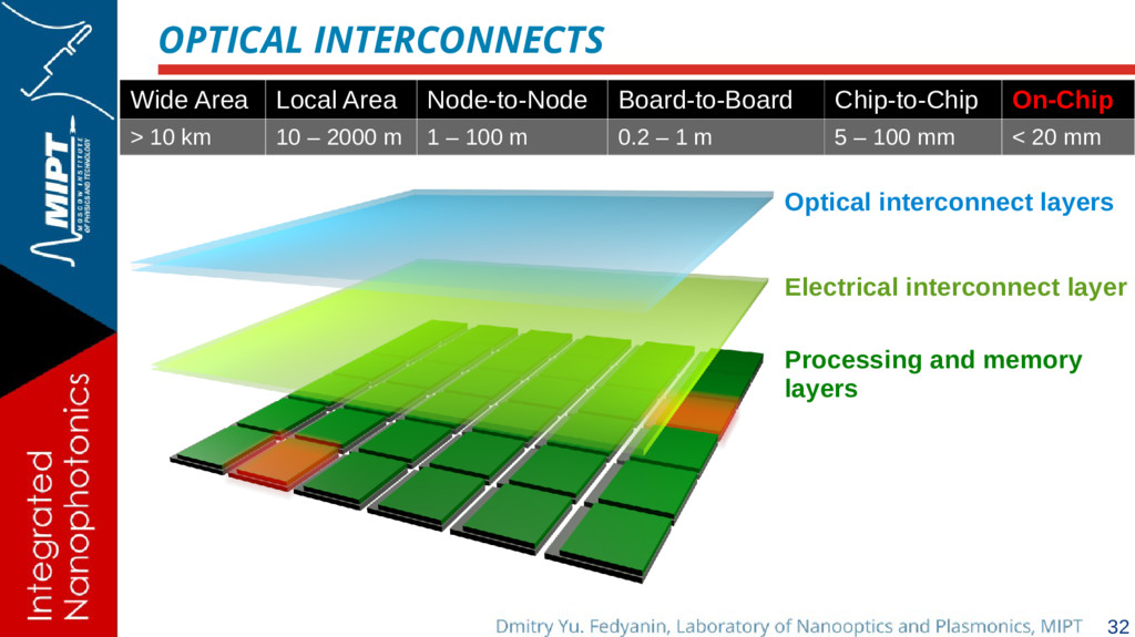
On-Chip > 10 km 10 – 2000 m 1 – 100 m 0.2 – 1 m 5 – 100 mm < 20 mm Optical interconnect layers Electrical interconnect layer Processing and memory layers
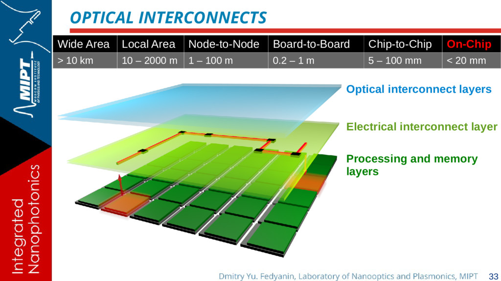
On-Chip > 10 km 10 – 2000 m 1 – 100 m 0.2 – 1 m 5 – 100 mm < 20 mm Optical interconnect layers Electrical interconnect layer Processing and memory layers
On-Chip > 10 km 10 – 2000 m 1 – 100 m 0.2 – 1 m 5 – 100 mm < 20 mm Optical interconnect layers Electrical interconnect layer Processing and memory layers
On-Chip > 10 km 10 – 2000 m 1 – 100 m 0.2 – 1 m 5 – 100 mm < 20 mm Optical interconnect layers Electrical interconnect layer Processing and memory layers
On-Chip > 10 km 10 – 2000 m 1 – 100 m 0.2 – 1 m 5 – 100 mm < 20 mm Optical interconnect layers Electrical interconnect layer Processing and memory layers
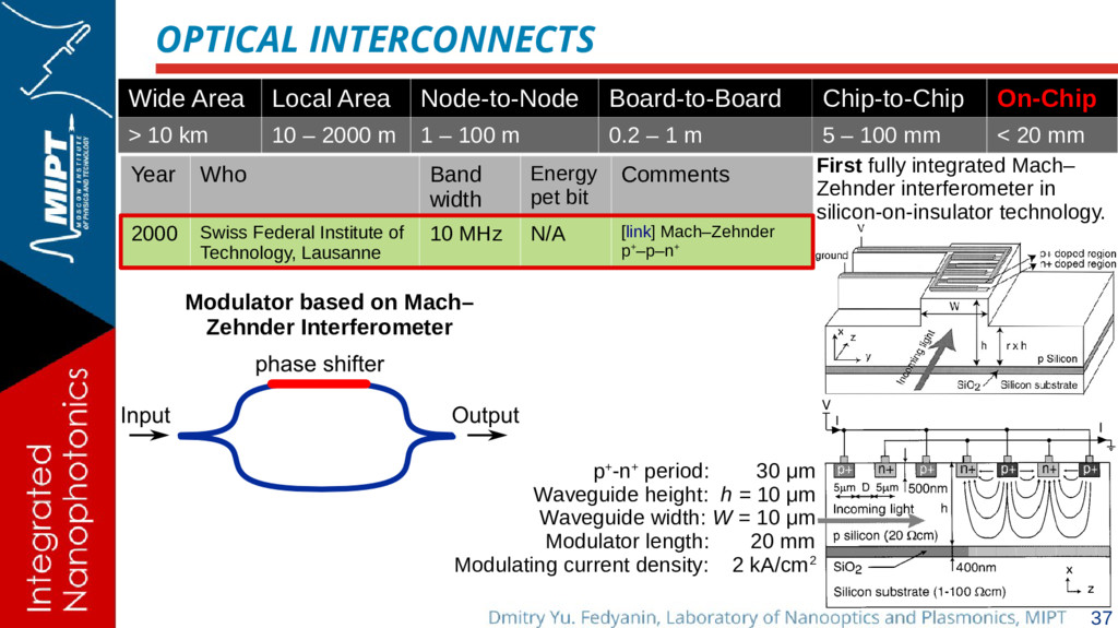
On-Chip > 10 km 10 – 2000 m 1 – 100 m 0.2 – 1 m 5 – 100 mm < 20 mm Year Who Band width Energy pet bit Comments 2000 Swiss Federal Institute of Technology, Lausanne 10 MHz N/A [link] Mach–Zehnder p+–p–n+ First fully integrated Mach– Zehnder interferometer in silicon-on-insulator technology. p+-n+ period: 30 μm Waveguide height: h = 10 μm Waveguide width: W = 10 μm Modulator length: 20 mm Modulating current density: 2 kA/cm2 Modulator based on Mach– Zehnder Interferometer
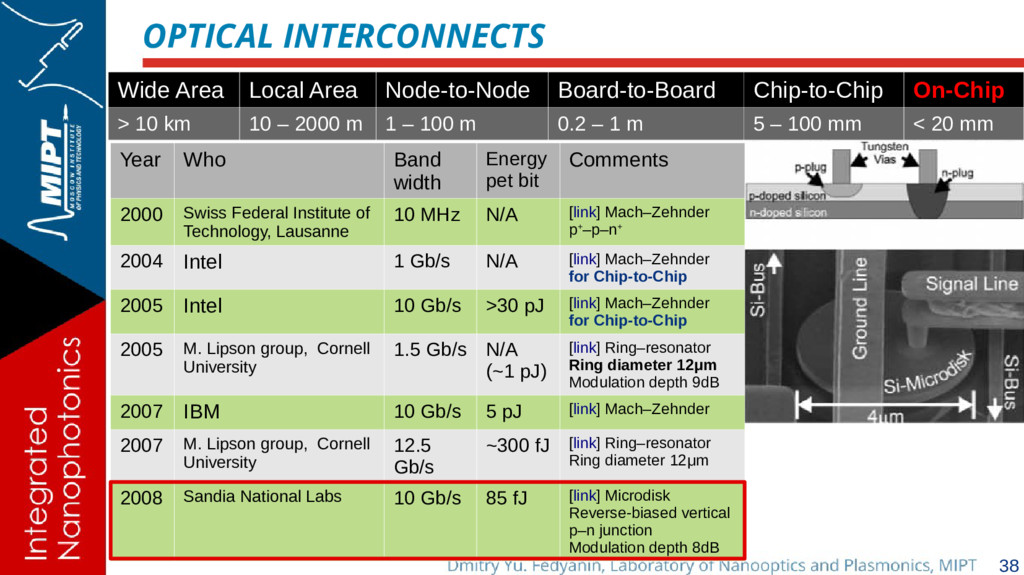
On-Chip > 10 km 10 – 2000 m 1 – 100 m 0.2 – 1 m 5 – 100 mm < 20 mm Year Who Band width Energy pet bit Comments 2000 Swiss Federal Institute of Technology, Lausanne 10 MHz N/A [link] Mach–Zehnder p+–p–n+ 2004 Intel 1 Gb/s N/A [link] Mach–Zehnder for Chip-to-Chip 2005 Intel 10 Gb/s >30 pJ [link] Mach–Zehnder for Chip-to-Chip 2005 M. Lipson group, Cornell University 1.5 Gb/s N/A (~1 pJ) [link] Ring–resonator Ring diameter 12μm Modulation depth 9dB 2007 IBM 10 Gb/s 5 pJ [link] Mach–Zehnder 2007 M. Lipson group, Cornell University 12.5 Gb/s ~300 fJ [link] Ring–resonator Ring diameter 12μm 2008 Sandia National Labs 10 Gb/s 85 fJ [link] Microdisk Reverse-biased vertical p–n junction Modulation depth 8dB
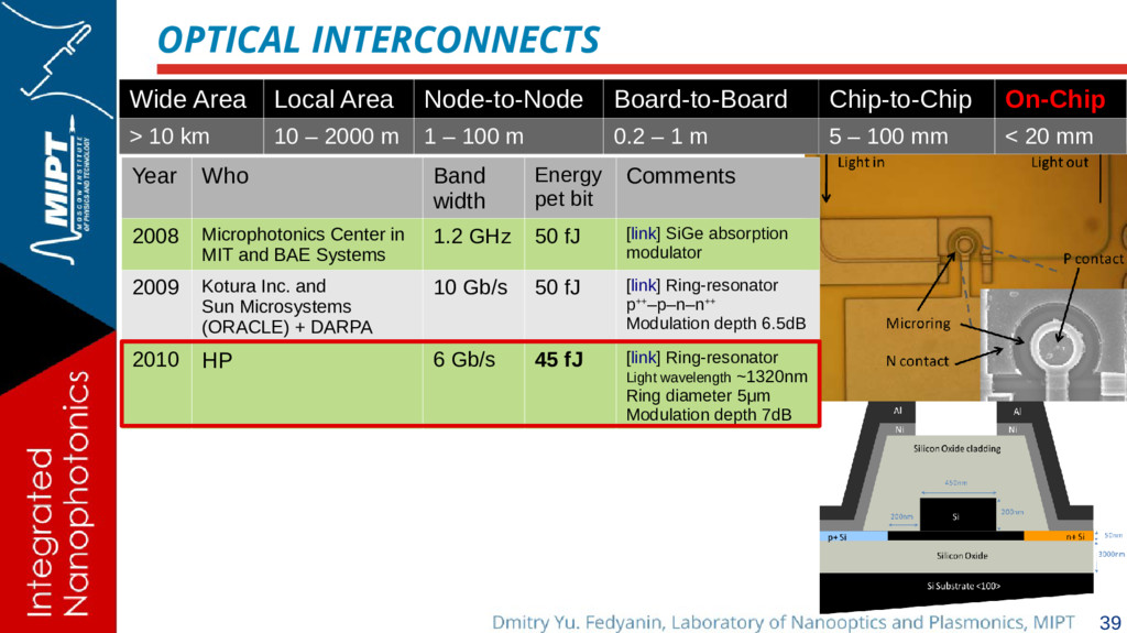
On-Chip > 10 km 10 – 2000 m 1 – 100 m 0.2 – 1 m 5 – 100 mm < 20 mm Year Who Band width Energy pet bit Comments 2008 Microphotonics Center in MIT and BAE Systems 1.2 GHz 50 fJ [link] SiGe absorption modulator 2009 Kotura Inc. and Sun Microsystems (ORACLE) + DARPA 10 Gb/s 50 fJ [link] Ring-resonator p++–p–n–n++ Modulation depth 6.5dB 2010 HP 6 Gb/s 45 fJ [link] Ring-resonator Light wavelength ~1320nm Ring diameter 5μm Modulation depth 7dB
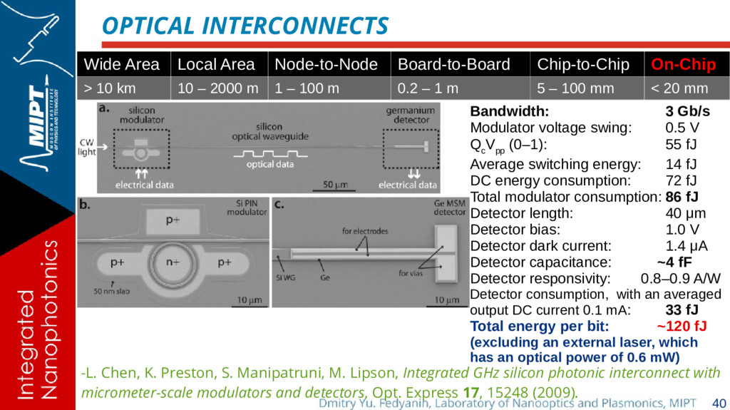
On-Chip > 10 km 10 – 2000 m 1 – 100 m 0.2 – 1 m 5 – 100 mm < 20 mm -L. Chen, K. Preston, S. Manipatruni, M. Lipson, Integrated GHz silicon photonic interconnect with micrometer-scale modulators and detectors, Opt. Express 17, 15248 (2009). Bandwidth: 3 Gb/s Modulator voltage swing: 0.5 V Q c V pp (0–1): 55 fJ Average switching energy: 14 fJ DC energy consumption: 72 fJ Total modulator consumption: 86 fJ Detector length: 40 μm Detector bias: 1.0 V Detector dark current: 1.4 μA Detector capacitance: ~4 fF Detector responsivity: 0.8–0.9 A/W Detector consumption, with an averaged output DC current 0.1 mA: 33 fJ Total energy per bit: ~120 fJ (excluding an external laser, which has an optical power of 0.6 mW)
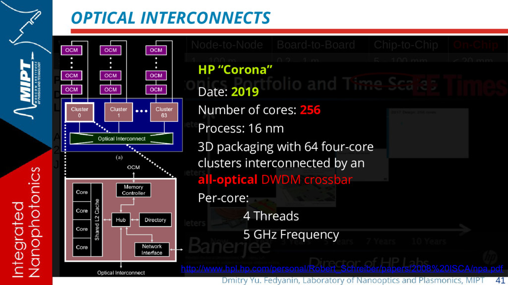
On-Chip > 10 km 10 – 2000 m 1 – 100 m 0.2 – 1 m 5 – 100 mm < 20 mm Prith Banerjee Director HP Labs At DesignCon 2012, January 2012 HP “Corona” Date: 2019 Number of cores: 256 Process: 16 nm 3D packaging with 64 four-core clusters interconnected by an all-optical DWDM crossbar Per-core: 4 Threads 5 GHz Frequency http://www.hpl.hp.com/personal/Robert_Schreiber/papers/2008%20ISCA/npa.pdf
integrated (nano)photonics, which are out of the scope of this lecture: • Chemical and biosensing • Graphics processors • Ultrafast encryption • Quantum optics: from quantum cryptography to quantum computers • Deep learning • All-optical microprocessor
function. Electromagnetic energy and its relation to the dielectric function. Group velocity and energy velocity. Transmission/reflection at the interface.