Techniques de conception et applications sur FPGAs partiellement reconfigurables Jean-Philippe Delahaye Doctorant à Supélec SUPELEC - Campus de Rennes - FRANCE SCEE team – Signal, Communication and Embedded Systems IETR – UMR 6164 Institut d’Electronique et de Télécommunications de Rennes
conception et Application sur FPGA partiellement reconfigurable • Introduction • Flot de conception Modular Design • La reconfiguration partielle de FPGA • L’ application P-HAL • Conclusion
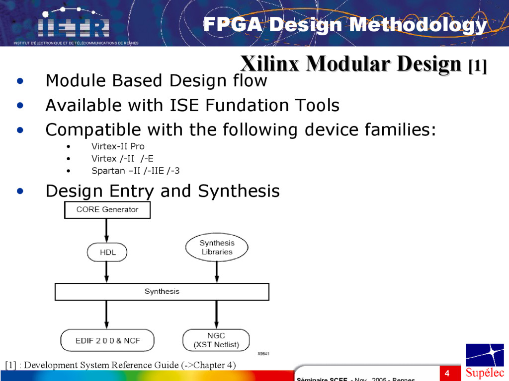
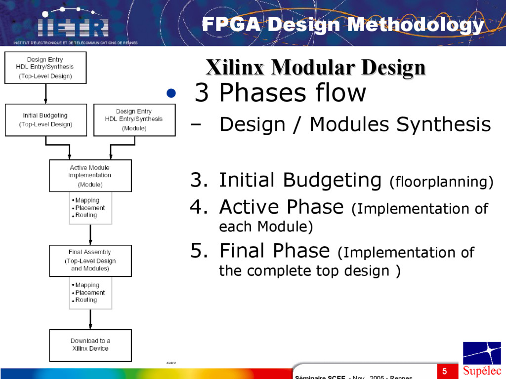
Design Xilinx Modular Design [1] [1] FPGA Design Methodology • Module Based Design flow • Available with ISE Fundation Tools • Compatible with the following device families: • Virtex-II Pro • Virtex /-II /-E • Spartan –II /-IIE /-3 • Design Entry and Synthesis [1] : Development System Reference Guide (->Chapter 4)
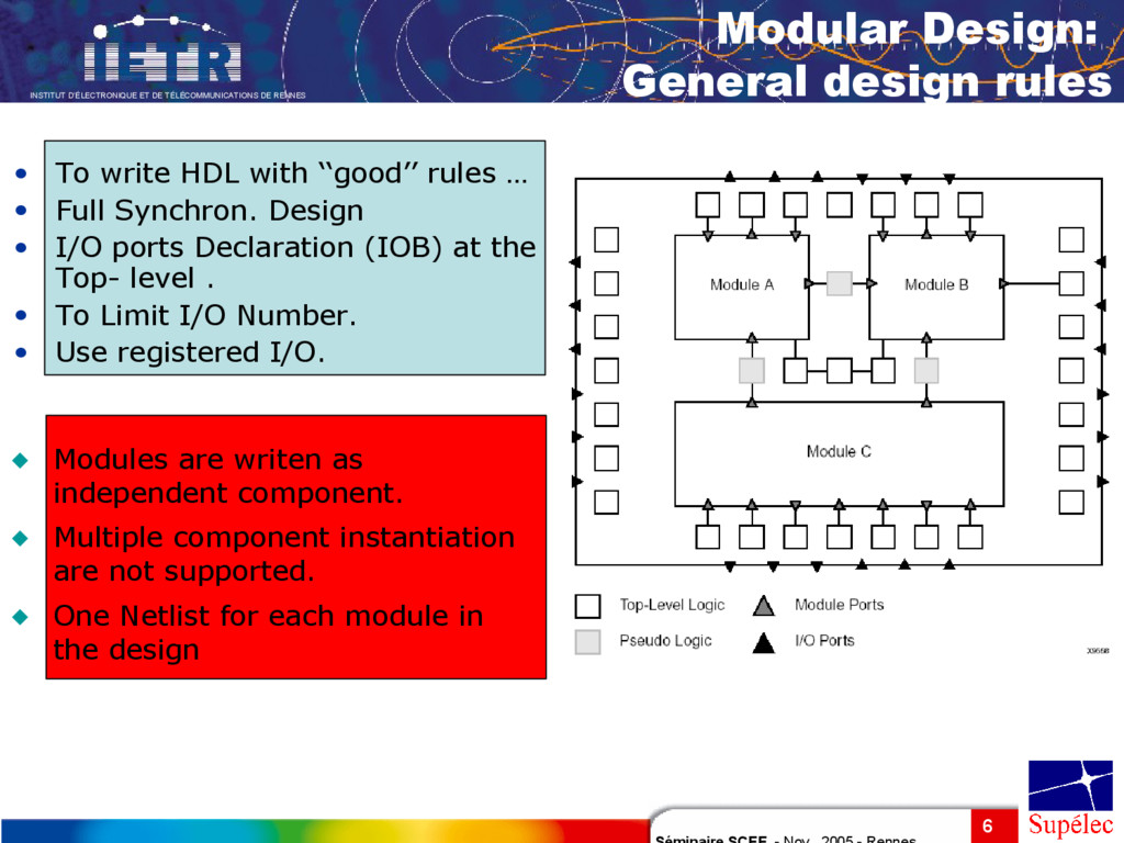
write HDL with ‘‘good’’ rules … • Full Synchron. Design • I/O ports Declaration (IOB) at the Top- level . • To Limit I/O Number. • Use registered I/O. Modular Design: General design rules x Modules are writen as independent component. x Multiple component instantiation are not supported. x One Netlist for each module in the design
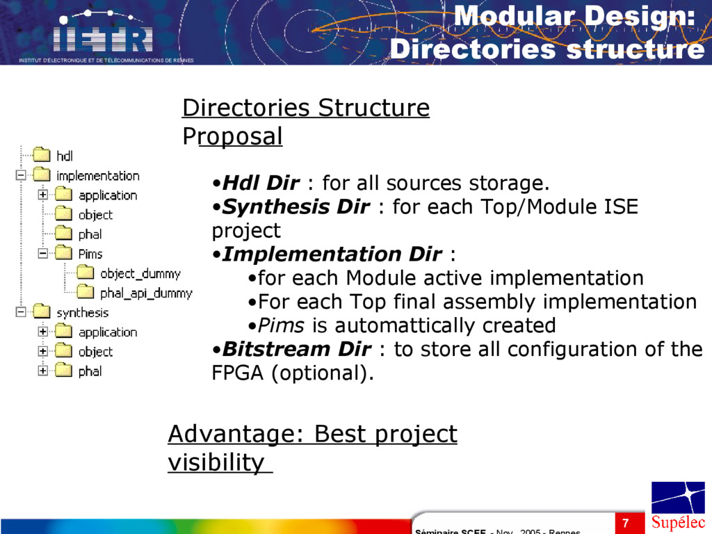
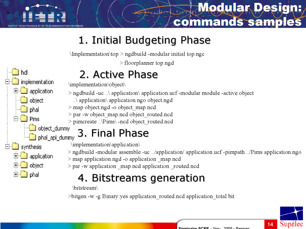
Proposal Modular Design: Directories structure •Hdl Dir : for all sources storage. •Synthesis Dir : for each Top/Module ISE project •Implementation Dir : •for each Module active implementation •For each Top final assembly implementation •Pims is automattically created •Bitstream Dir : to store all configuration of the FPGA (optional). Advantage: Best project visibility
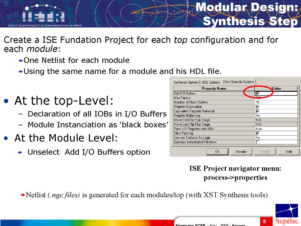
Synthesis Step • At the top-Level: – Declaration of all IOBs in I/O Buffers – Module Instanciation as ‘black boxes’ • At the Module Level: ² Unselect Add I/O Buffers option Create a ISE Fundation Project for each top configuration and for each module: ² One Netlist for each module ² Using the same name for a module and his HDL file. ²Netlist (.ngc files) is generated for each modules/top (with XST Synthesis tools) ISE Project navigator menu: process->properties
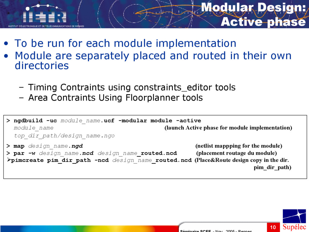
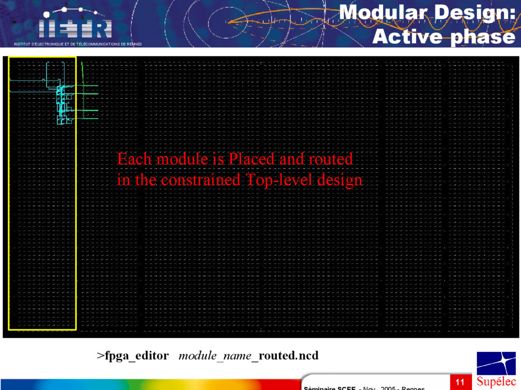
-uc module_name.ucf -modular module -active module_name (launch Active phase for module implementation) top_dir_path/design_name.ngo > map design_name.ngd (netlist mappping for the module) > par -w design_name.ncd design_name_routed.ncd (placement routage du module) pimcreate pim_dir_path -ncd design_name_routed.ncd (Place&Route design copy in the dir. pim_dir_path) • To be run for each module implementation • Module are separately placed and routed in their own directories – Timing Contraints using constraints_editor tools – Area Contraints Using Floorplanner tools Modular Design: Active phase
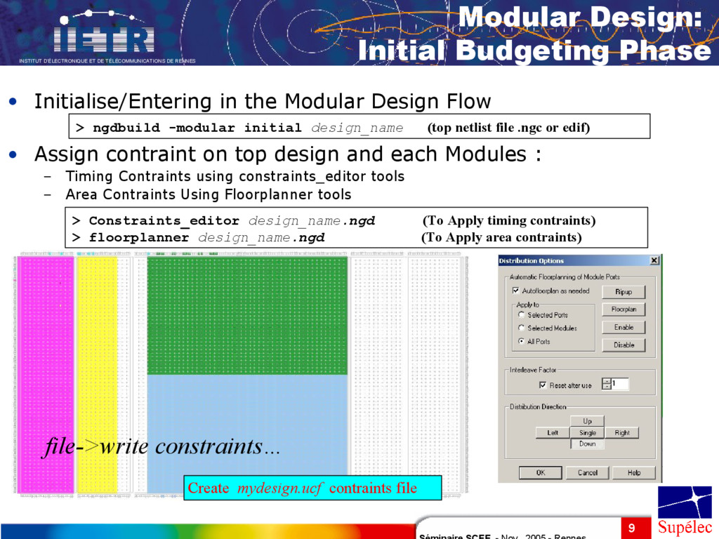
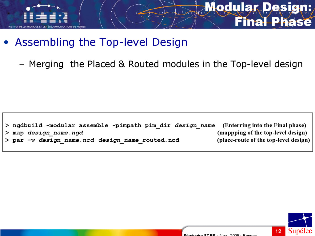
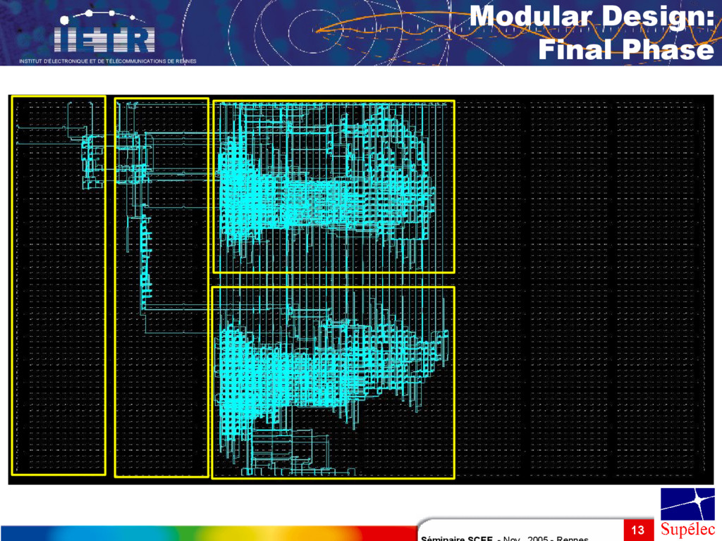
Final Phase > ngdbuild -modular assemble -pimpath pim_dir design_name (Enterring into the Final phase) > map design_name.ngd (mappping of the top-level design) > par -w design_name.ncd design_name_routed.ncd (place-route of the top-level design) • Assembling the Top-level Design – Merging the Placed & Routed modules in the Top-level design
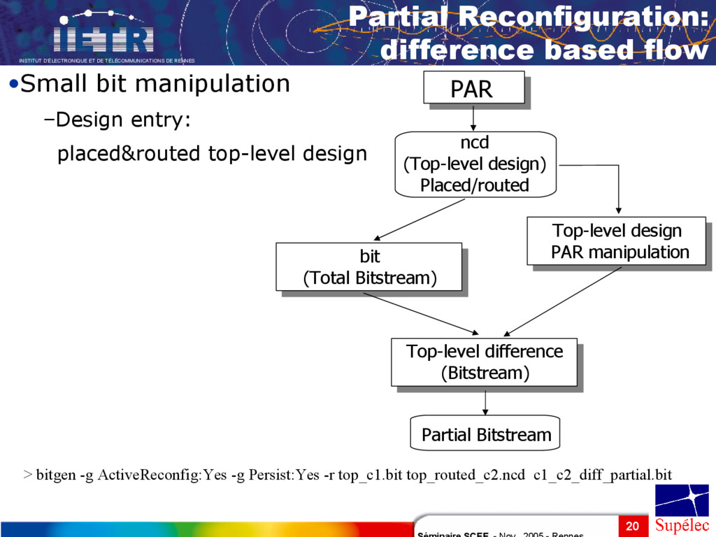
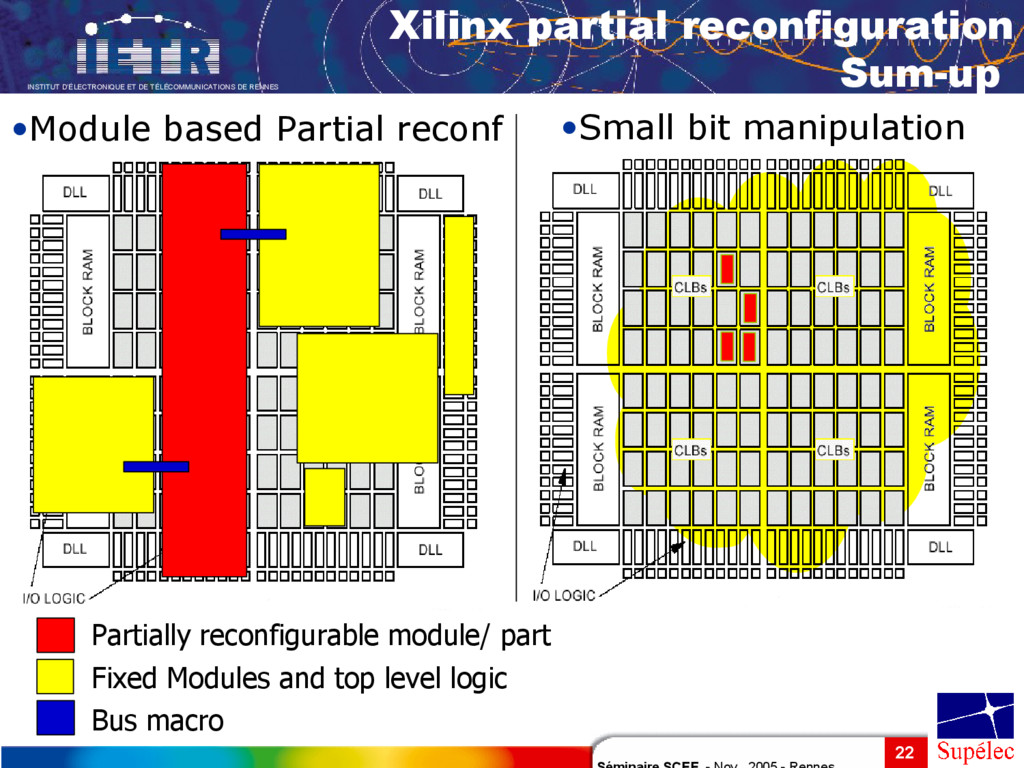
Flows for Partial bitstream [4]: – Module Based reconfiguration • Mandatory based on Modular Design – Difference based reconfiguration. • For small bit manipulation • 2 types of partial reconfiguration – multi-columns modules without comm. – multi-columns with inter-module communication (-> Using bus macro) [4] XAPP290: Two Flows for Partial Reconfiguration Partial Reconfiguration: Overview
Constraints on a module : – minimal reconfigurable area 4CLB rows. (->Bus macro) • The IOBs adjoining the reconfigurable area are dedicated to this area. • All communications throw Bus Macro. • The Same Overall I/O declaration in each module configuration – ex: PRmoduleA uses 5 e/s E1:{clk,in1,in2,in3,out1} – PRmoduleB uses 4 e/s E2:{clk,in1,in4,out2} – Then I/O to declare in each configuration are : – E1 U E2 : {CLK, in1, in2,in3, in4,out1,out2} Partial Reconfiguration: Module based flow
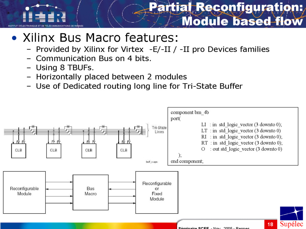
Bus Macro features: – Provided by Xilinx for Virtex -E/-II / -II pro Devices families – Communication Bus on 4 bits. – Using 8 TBUFs. – Horizontally placed between 2 modules – Use of Dedicated routing long line for Tri-State Buffer Partial Reconfiguration: Module based flow component bm_4b port( LI : in std_logic_vector (3 downto 0); LT : in std_logic_vector (3 downto 0) RI : in std_logic_vector (3 downto 0); RT : in std_logic_vector (3 downto 0); O : out std_logic_vector (3 downto 0) ); end component;
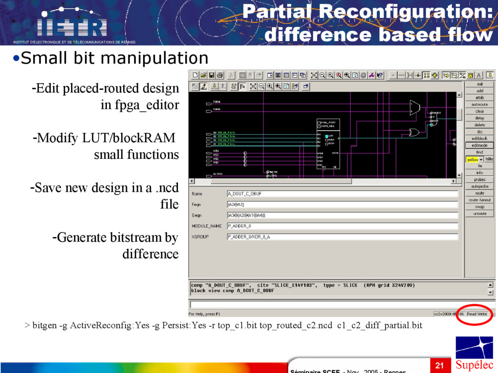
design in fpga_editor -Modify LUT/blockRAM small functions -Save new design in a .ncd file -Generate bitstream by difference > bitgen -g ActiveReconfig:Yes -g Persist:Yes -r top_c1.bit top_routed_c2.ncd c1_c2_diff_partial.bit Partial Reconfiguration: difference based flow •Small bit manipulation
reconfiguration Sum-up Partially reconfigurable module/ part Fixed Modules and top level logic Bus macro •Small bit manipulation •Module based Partial reconf
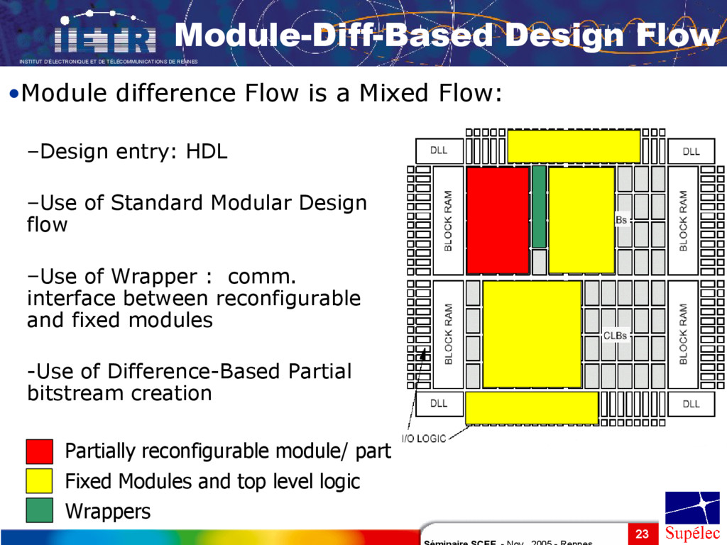
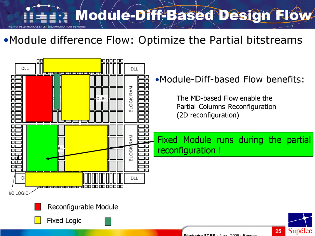
Flow Partially reconfigurable module/ part Fixed Modules and top level logic Wrappers •Module difference Flow is a Mixed Flow: –Design entry: HDL –Use of Standard Modular Design flow –Use of Wrapper : comm. interface between reconfigurable and fixed modules -Use of Difference-Based Partial bitstream creation
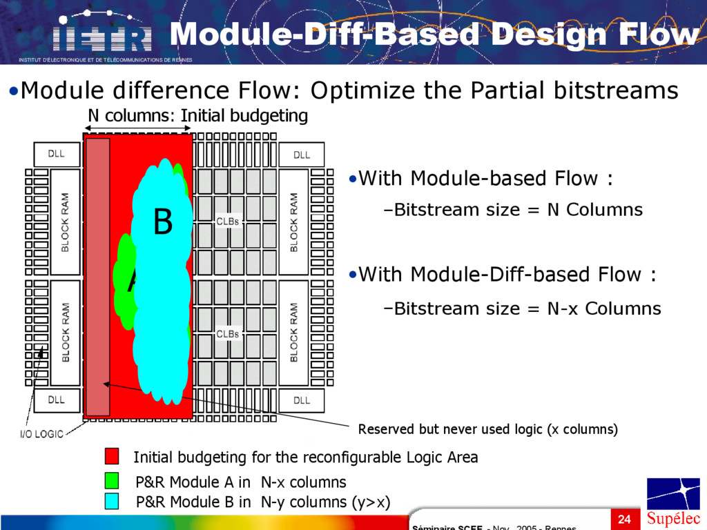
Initial budgeting Initial budgeting for the reconfigurable Logic Area Module-Diff-Based Design Flow •Module difference Flow: Optimize the Partial bitstreams Reserved but never used logic (x columns) •With Module-based Flow : –Bitstream size = N Columns •With Module-Diff-based Flow : –Bitstream size = N-x Columns A P&R Module A in N-x columns B P&R Module B in N-y columns (y>x)
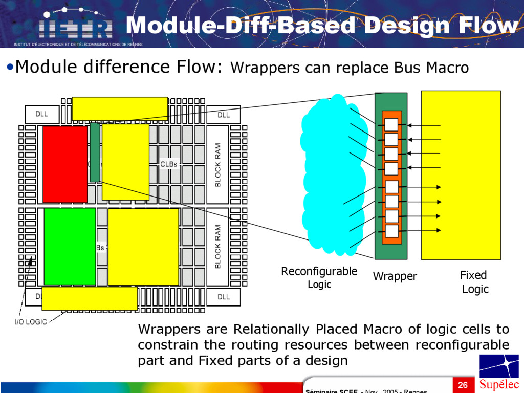
Flow •Module difference Flow: Wrappers can replace Bus Macro Reconfigurable Logic Fixed Logic Wrappers are Relationally Placed Macro of logic cells to constrain the routing resources between reconfigurable part and Fixed parts of a design Wrapper
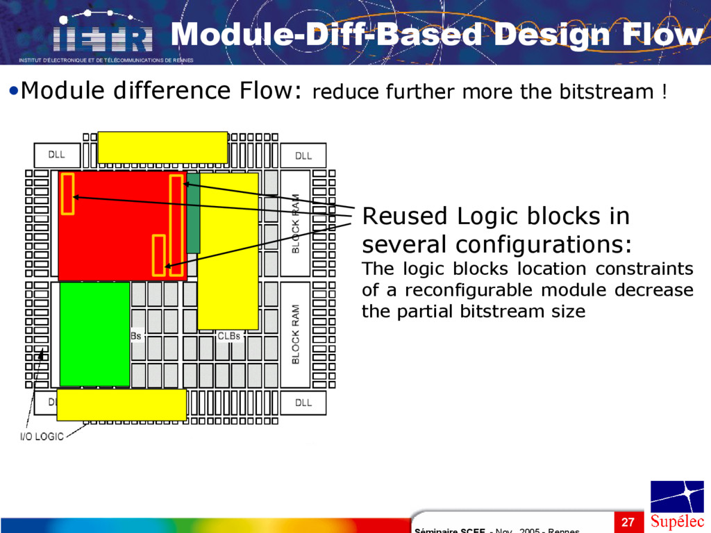
Flow •Module difference Flow: reduce further more the bitstream ! Reused Logic blocks in several configurations: The logic blocks location constraints of a reconfigurable module decrease the partial bitstream size
Guides: available on c:\xilinx\doc\english\ [1] : Development System Reference Guide (dev.pdf) [2] : Constraint Guide (cgd.pdf) [3] : Libraries Guide (lib.pdf) - Xilinx XAPPs: [4] XAPP290: Two Flows for Partial Reconfiguration [5] XAPP151: Virtex Series Configuration Architecture User Guide - Support: www.support.xilinx.com - From the web: Tutorials: http://appsrv.cse.cuhk.edu.hk/~ceg5010/tut/fpga.htm http://ic2.epfl.ch/~gmermoud/files/publications/DPRtutorial.pdf Mailing list: http://www.itee.uq.edu.au/~listarch/partial-reconfig/archive/2005/09/index.html Main Technical documentations Starting with Partial Reconfiguration
Concepts, Architecture, Definitions, Rules, … Xavier Revés, Antoni Gelonch, Vuk Marojevic, Radio Communications Group Universitat Politècnica de Catalunya P-HAL: Platform-Hardware Abstraction Layer [1] [1] ''FPGA's Middleware for Software Defined Radio Applications'', X. Revés, V. Marojevic, R. Ferrús, and A. Gelonch, 15th International Conference on Field Programmable Logic and Applications (FPL’05), Tampere, Finland, 24-26 Aug. 2005
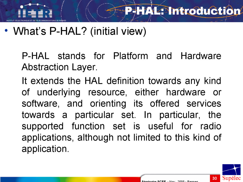
P-HAL stands for Platform and Hardware Abstraction Layer. It extends the HAL definition towards any kind of underlying resource, either hardware or software, and orienting its offered services towards a particular set. In particular, the supported function set is useful for radio applications, although not limited to this kind of application. • What’s P-HAL? (initial view)
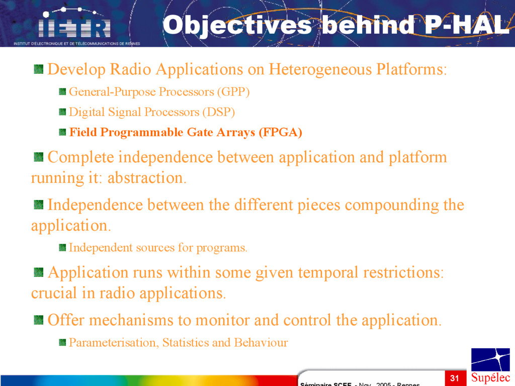
P-HAL Develop Radio Applications on Heterogeneous Platforms: General-Purpose Processors (GPP) Digital Signal Processors (DSP) Field Programmable Gate Arrays (FPGA) Complete independence between application and platform running it: abstraction. Independence between the different pieces compounding the application. Independent sources for programs. Application runs within some given temporal restrictions: crucial in radio applications. Offer mechanisms to monitor and control the application. Parameterisation, Statistics and Behaviour
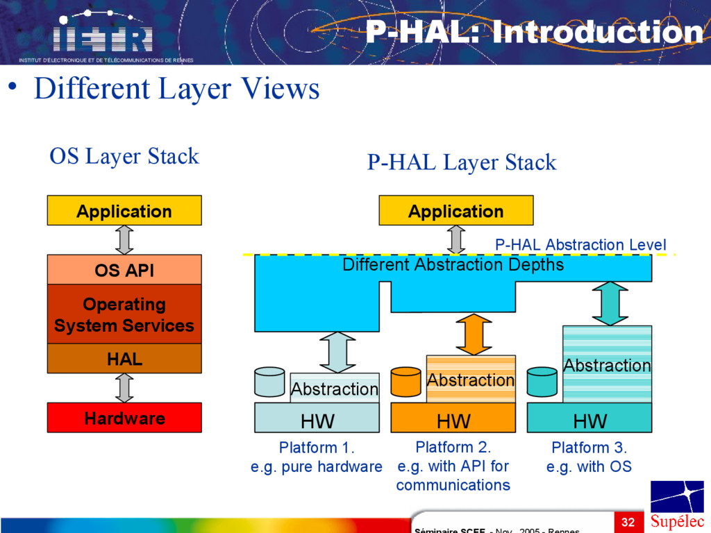
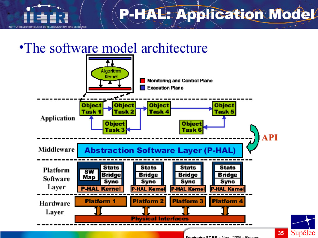
Operating System Services OS API Application OS Layer Stack Platform 2. e.g. with API for communications HW HW HW Abstraction Abstraction Abstraction Different Abstraction Depths Application P-HAL Layer Stack P-HAL Abstraction Level Platform 3. e.g. with OS Platform 1. e.g. pure hardware P-HAL: Introduction • Different Layer Views
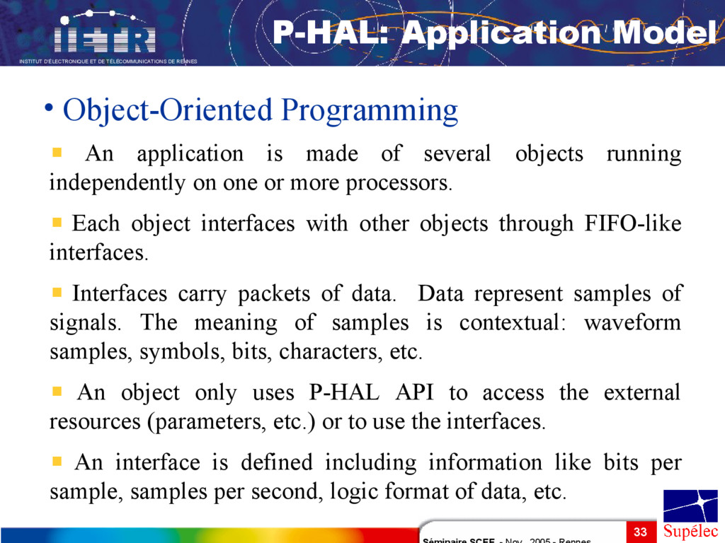
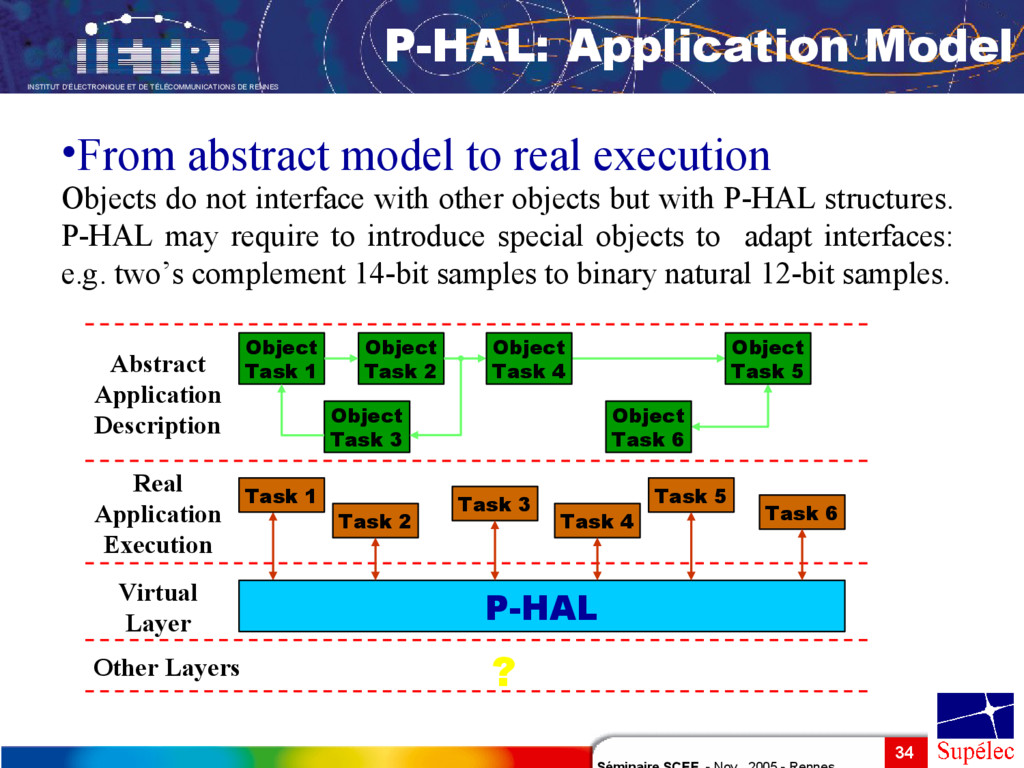
Programming An application is made of several objects running independently on one or more processors. Each object interfaces with other objects through FIFO-like interfaces. Interfaces carry packets of data. Data represent samples of signals. The meaning of samples is contextual: waveform samples, symbols, bits, characters, etc. An object only uses P-HAL API to access the external resources (parameters, etc.) or to use the interfaces. An interface is defined including information like bits per sample, samples per second, logic format of data, etc. P-HAL: Application Model
model to real execution Objects do not interface with other objects but with P-HAL structures. P-HAL may require to introduce special objects to adapt interfaces: e.g. two’s complement 14-bit samples to binary natural 12-bit samples. Virtual Layer P-HAL Task 1 Task 2 Task 3 Task 4 Task 5 Task 6 Real Application Execution Abstract Application Description Object Task 1 Object Task 2 Object Task 3 Object Task 4 Object Task 6 Object Task 5 ? Other Layers P-HAL: Application Model
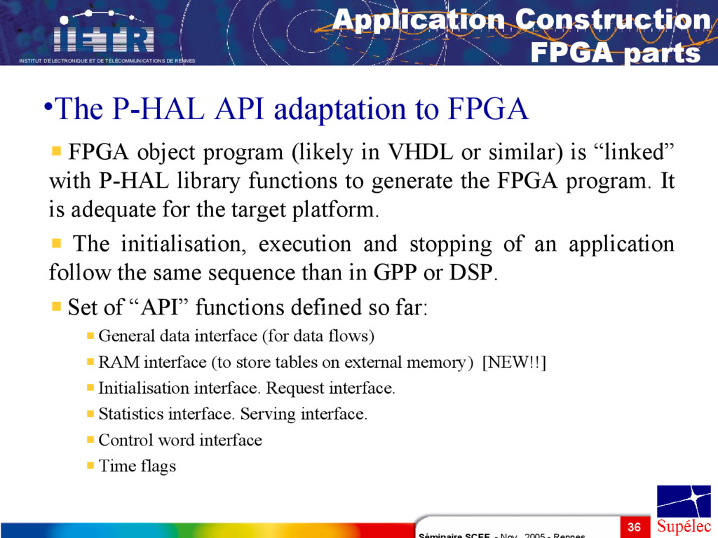
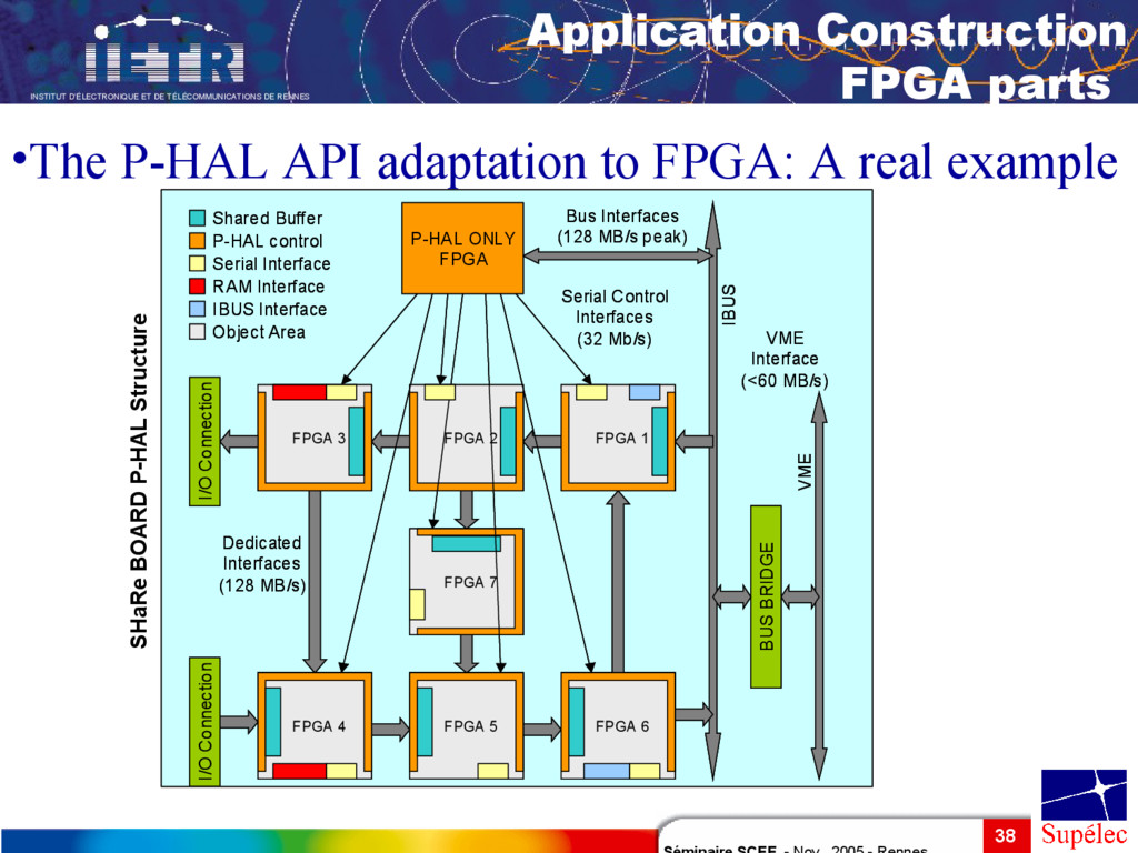
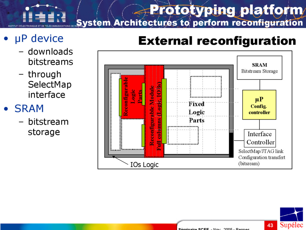
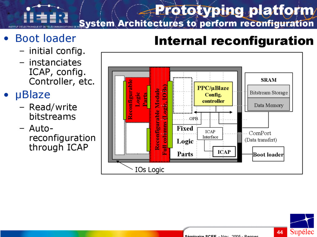
program (likely in VHDL or similar) is “linked” with P-HAL library functions to generate the FPGA program. It is adequate for the target platform. The initialisation, execution and stopping of an application follow the same sequence than in GPP or DSP. Set of “API” functions defined so far: General data interface (for data flows) RAM interface (to store tables on external memory) [NEW!!] Initialisation interface. Request interface. Statistics interface. Serving interface. Control word interface Time flags Application Construction FPGA parts •The P-HAL API adaptation to FPGA
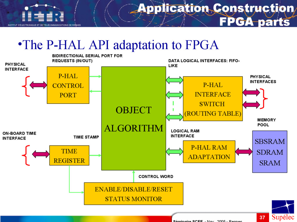
P-HAL INTERFACE SWITCH (ROUTING TABLE) DATA LOGICAL INTERFACES: FIFO- LIKE PHYSICAL INTERFACES P-HAL RAM ADAPTATION LOGICAL RAM INTERFACE SBSRAM SDRAM SRAM MEMORY POOL ENABLE/DISABLE/RESET STATUS MONITOR P-HAL CONTROL PORT CONTROL WORD BIDIRECTIONAL SERIAL PORT FOR REQUESTS (IN/OUT) PHYSICAL INTERFACE TIME REGISTER TIME STAMP ON-BOARD TIME INTERFACE •The P-HAL API adaptation to FPGA Application Construction FPGA parts
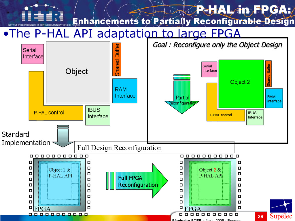
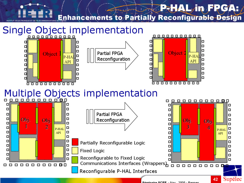
Object RAM Interface Shared Buffer Serial Interface P-HAL control FPGA Object 1 & P-HAL API Standard Implementation Full Design Reconfiguration FPGA Object 2 & P-HAL API Full FPGA Reconfiguration IBUS Interface Object 1 RAM Interface Shared Buffer Serial Interface P-HAL control Goal : Reconfigure only the Object Design Goal : Reconfigure only the Object Design Object 2 Partial Reconfiguration •The P-HAL API adaptation to large FPGA P-HAL in FPGA: Enhancements to Partially Reconfigurable Design
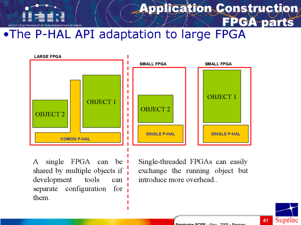
COMON P-HAL OBJECT 1 OBJECT 2 SMALL FPGA SINGLE P-HAL OBJECT 2 SMALL FPGA SINGLE P-HAL OBJECT 1 A single FPGA can be shared by multiple objects if development tools can separate configuration for them. Single-threaded FPGAs can easily exchange the running object but introduce more overhead.. Application Construction FPGA parts •The P-HAL API adaptation to large FPGA