Upgrade to Pro — share decks privately, control downloads, hide ads and more …

Design principles for emerging chalcogenide photovoltaics

Design principles for emerging chalcogenide photovoltaics

Talk given at MATSUS23, 2023

Alex Ganose

March 10, 2023
Tweet

More Decks by Alex Ganose

Other Decks in Research

Transcript

  1. ns2 materials have desired properties Post transition metals with N–2

    electronic configuration Polarisable, large dielectric & low effective masses • carrier separation (weak excitons) • transport (low scattering) Pb2+ Sn2+ Ge2+ Sb3+ Bi3+
  2. PbS QDs Eg = 0.29 eV 10.5% PbS-Bi2 S3 Nanoheterojunction

    4.9% Bi2 S3 Eg = 1.55 eV 3.3% PbS and Bi2 S3
  3. Many compounds in the Pb–Bi–S system Craig, Miner, Deposita (1967)

    306, 278–306 Malika et al., Results in Physics (2013) 3, 30–37 Lots of structural data, not much characterisation
  4. Band gap increases with Bi content Pb6 Bi2 S9 Eg

    = 0.25 eV Pb2 Bi2 S5 Eg = 0.69 eV PbBi2 S4 Eg = 1.32 eV Chem. Mater. 29, 5156–5167 (2017) increasing Bi
  5. Complex electronic structure trend Chem. Mater. 29, 5156–5167 (2017) Pb6

    Bi2 S9 me = 0.19 mh = 0.21 ε∞ = 18.4 Pb2 Bi2 S5 me = 0.57 mh = 2.47 ε∞ = 13.6 PbBi2 S4 me = 0.35 mh = 0.68 ε∞ = 14.7 increasing Bi
  6. Theoretical efficiencies with Bi content Chem. Mater. 29, 5156–5167 (2017)

    PbBi2 S4 offers compromise between effective masses, band gap and indirect character Largest SLME for 200 nm thin film increasing Bi
  7. Calculating defects from first principles Goyal, Gorai, Peng, Lany, Stevanovic,

    Comput. Mater. Sci. 130, 1 (2017) Hess’ Law Products — reactants
  8. PbBi2 S4 shows complex defect chemistry Chem. Mater. 29, 5156–5167

    (2017) PbBi and BiPb dominate EF pinned ~0.9 eV above VBM
  9. V–VI–VII materials (bismuth chalcohalides) Family of BiChX materials exists BiOX

    (photocatalysts) BiTeX (quantum effects) BiSI & BiSeI (photovoltaics)
  10. BiSI & BiSeI Earth abundant & non-toxic Band gap ~1.57

    & 1.29 eV Ideal for pv! BUT Devices showed efficiencies ~0.002% Bi S I
  11. Both have ideal electronic structures BiSI Eg ind = 1.78

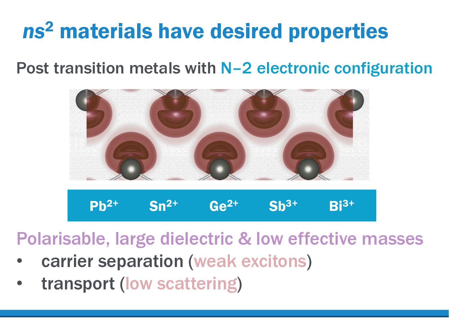
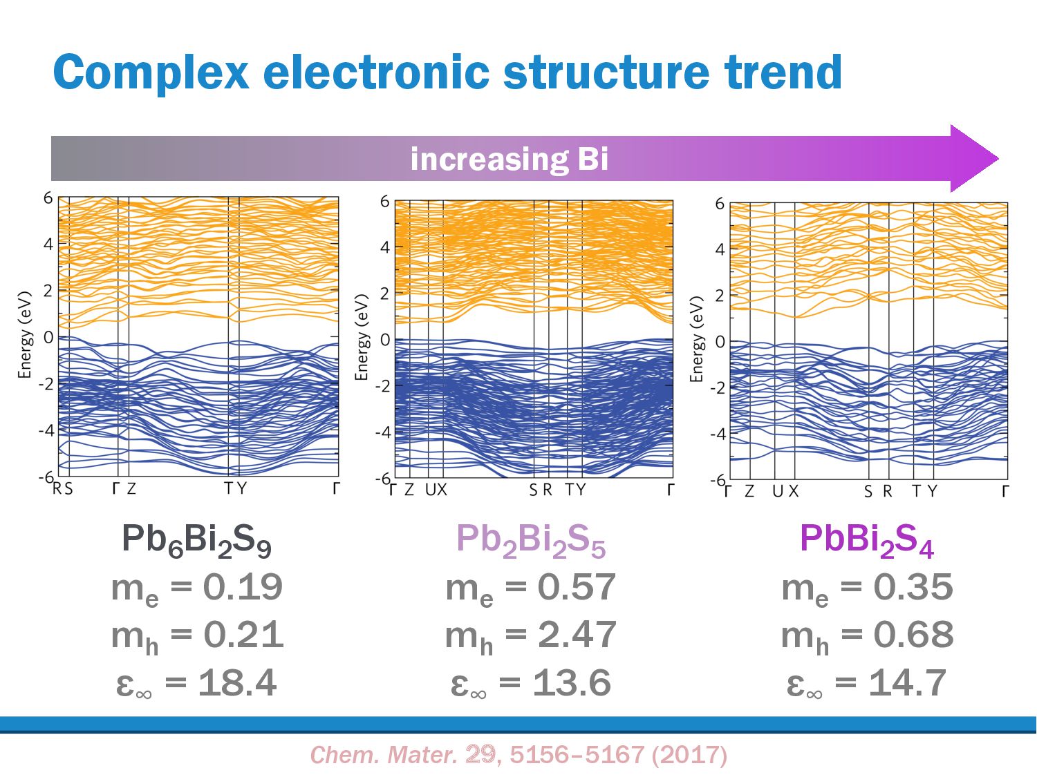
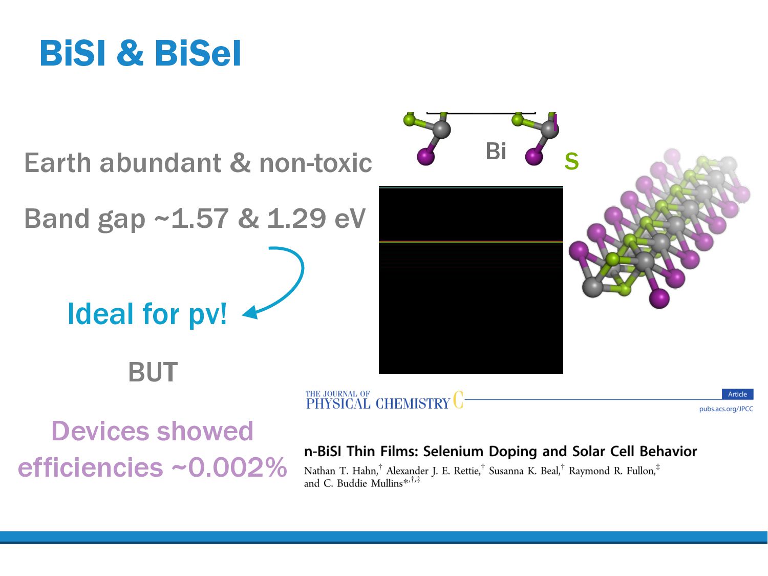
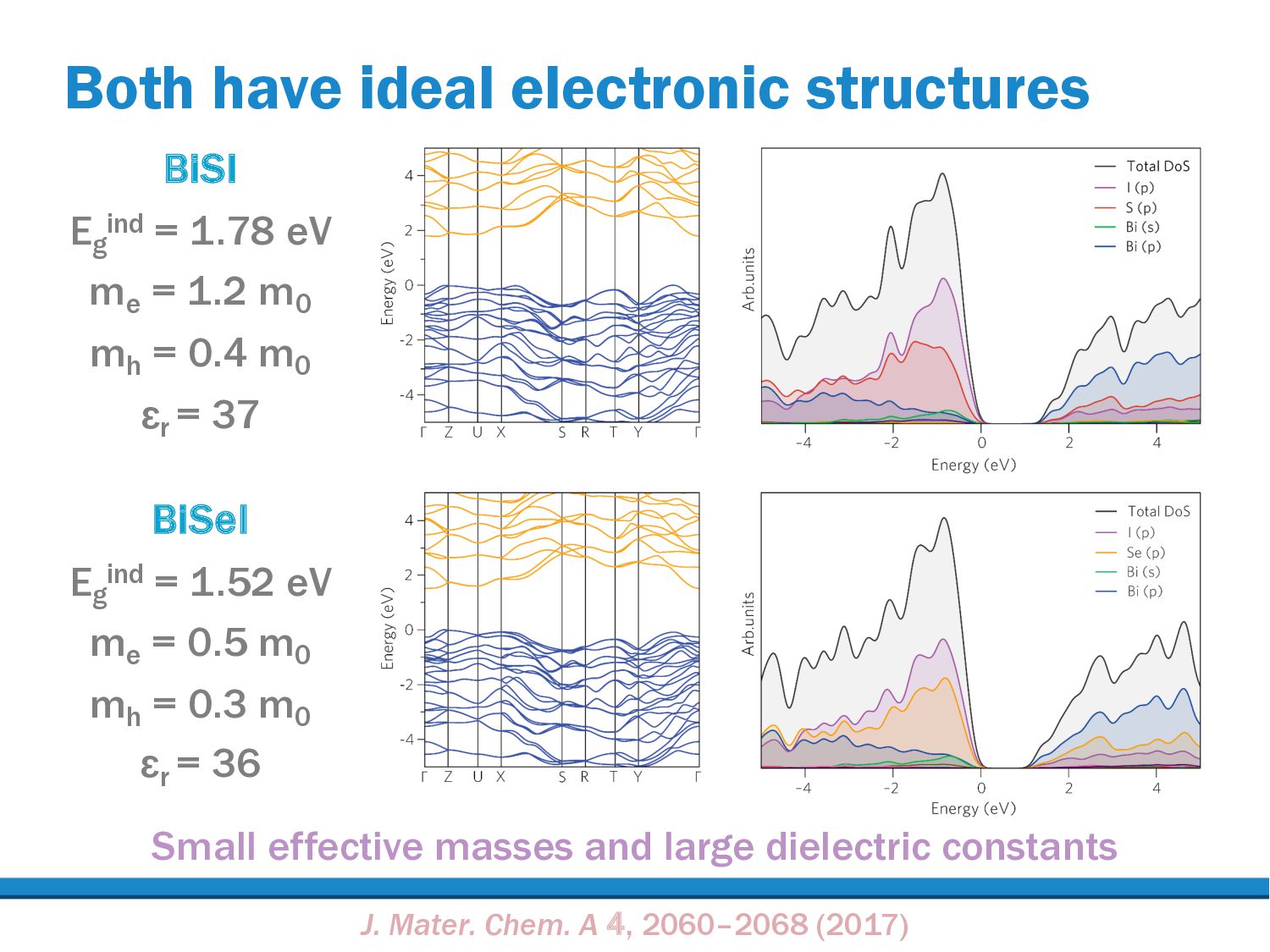
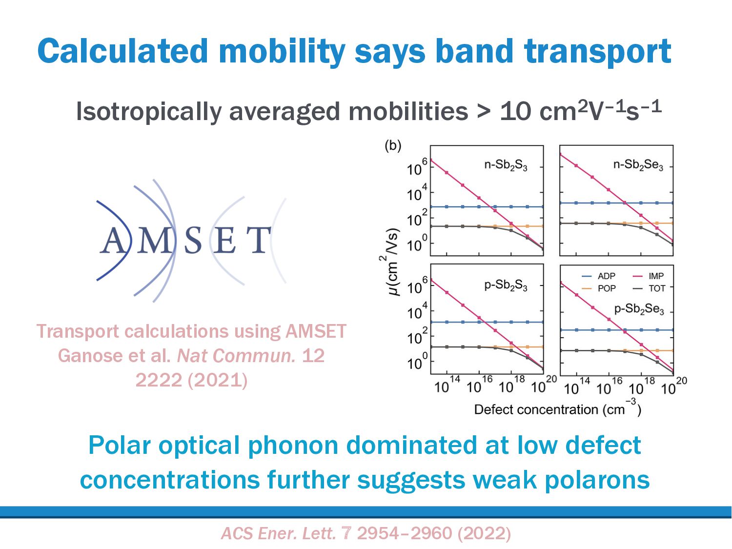
    eV me = 1.2 m0 mh = 0.4 m0 εr = 37 BiSeI Eg ind = 1.52 eV me = 0.5 m0 mh = 0.3 m0 εr = 36 Small effective masses and large dielectric constants J. Mater. Chem. A 4, 2060–2068 (2017)
  12. Large absorption & theoretical efficiency Chem. Mater. 30, 3827–3835 (2018)

    0 1 2 3 Energy (eV) 0 2x10⁴ Absor 0 250 500 750 1000 Thickness (nm) 0 10 20 30 SLME (%) RT 0K 0 1 2 3 Energy (eV) 0 2x10⁴ 5x10⁴ 8x10⁴ 1x10⁵ Absorption (cm−1) BiSeI BiSI 20 30 ) Very strong absorption due to high DOS High theoretical efficiencies ~26% at 200 nm
  13. Band alignments show very deep IPs Chem. Mater. 30, 3827–3835

    (2018) Hole contact limits open circuit voltage Electron contact limits electron diffusion Predict ITO and F8 as alternative contacts
  14. BiSI has deep n- and p-type defects Chem. Mater. 30,

    3827–3835 (2018) Ultra deep BiI and BiS acceptors Shallow IS donor SI compensation EF trapped in the band gap
  15. BiSeI shows similar defect chemistry Chem. Mater. 30, 3827–3835 (2018)

    SeI lower energy acceptor but deeper due to size mismatch Donors shallower due to lower CBM EF trapped in the band gap
  16. Synthesis control allows tuning SRH rate Chem. Mater. 30, 3827–3835

    (2018) Enables 107 cm–3s–1 reduction in recombination
  17. Sb2 Ch3 are also lone pair absorbers Sb2 Se3 shown

    efficiencies over 10% Both show “pseudo-1D” ribbon structures like BiSI Duan et al. Adv. Mater. 34, 2202969 (2022)
  18. Questions remain over self trapping Transient absorption attributed to carrier

    trapping 0.6 eV Stokes shift attributed to self-trapped excitons Yang et al. Nat. Commun. 10, 4540 (2019)
  19. Band vs hopping transport Wide range of measured mobilities led

    to debate over mechanism of carrier transport Comp Experimental mobility (cm2/Vs) e– h+ Sb2 S3 — 6.4 – 54 Sb2 Se3 15 0.69 – 45 ACS Ener. Lett. 7 2954–2960 (2022) Most measurements from thin films. Defect and grain boundary scattering likely
  20. Calculations suggest large polarons Schultz polaron radii extend over multiple

    unit cells Fröhlich coupling constant α between 0.5 – 6 indicates intermediate coupling ACS Ener. Lett. 7 2954–2960 (2022) Comp Fröhlich coupling Polaron Radius (Å) e– h+ e– h+ Sb2 S3 1.6 2.0 45.5 40.4 Sb2 Se3 1.3 2.1 40.4 31.9
  21. Calculated mobility says band transport Polar optical phonon dominated at

    low defect concentrations further suggests weak polarons Isotropically averaged mobilities > 10 cm2V–1s–1 ACS Ener. Lett. 7 2954–2960 (2022) Transport calculations using AMSET Ganose et al. Nat Commun. 12 2222 (2021)
  22. Does self-trapping occur? Explicit polaron calculations do not reveal self-trapping

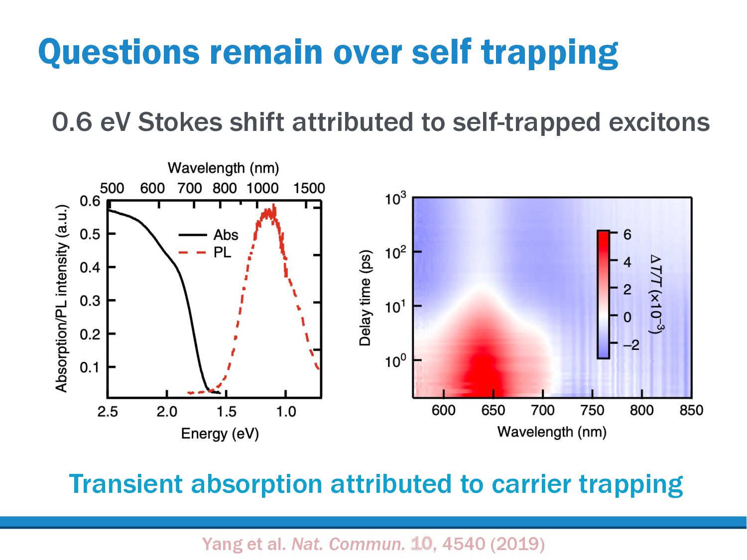
    How to explain experimental results? – Large Stokes shift in many materials w. deep defects – Subpicosecond decay characteristic of self-trapping (TA experiments suggest >10 ps) – TA signal persists to high carrier densities – could be photoinduced absorption or large trap density ACS Ener. Lett. 7 2954–2960 (2022) Conclusion: self-trapping unlikely!
  23. Conclusions Still searching for earth abundant & efficient photovoltaics Promising

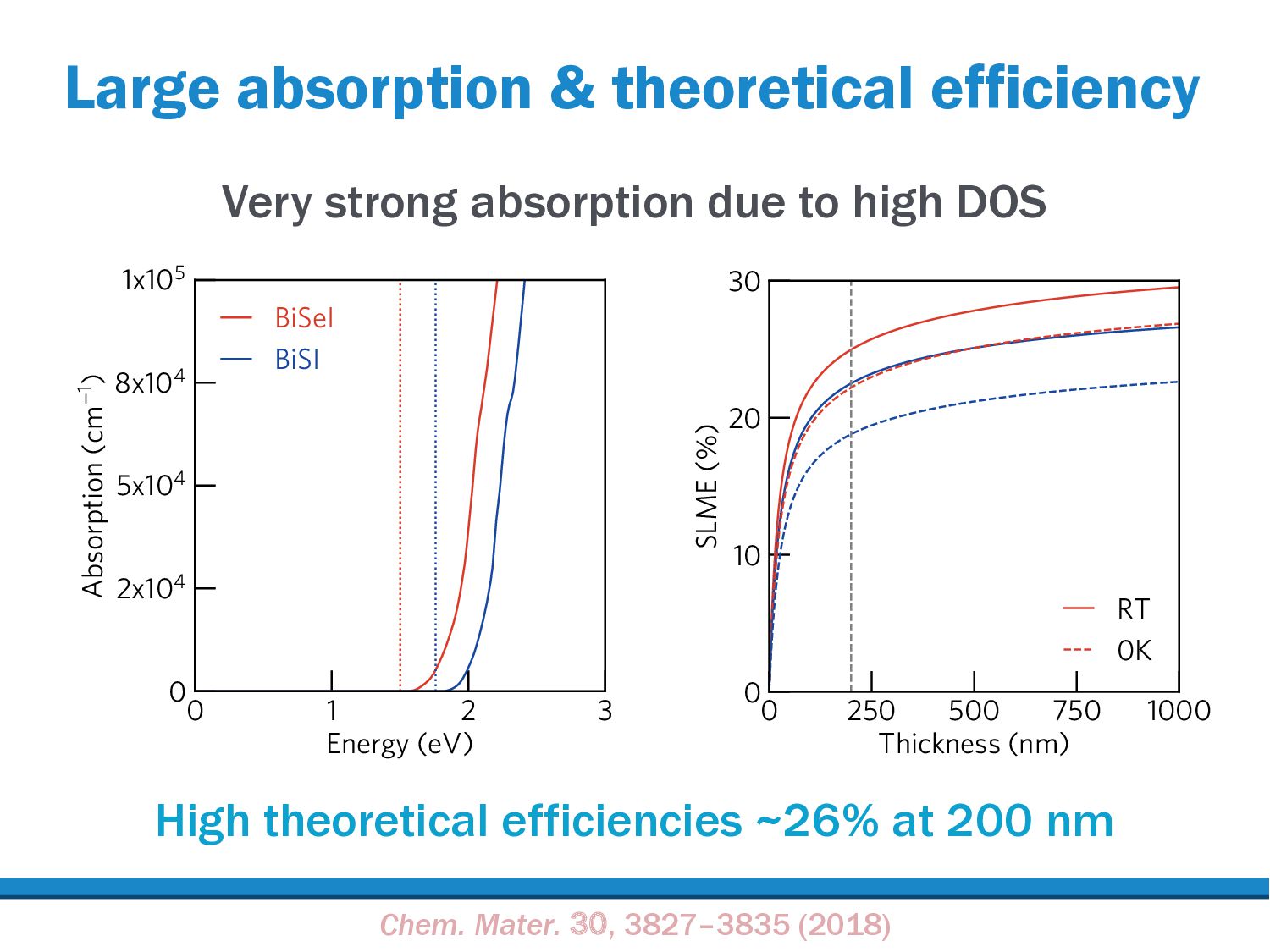
    candidate materials do exist Hard work needed to optimise properties (cannot expect same rate of progress as MAPbI3 ) A simple screening of electronic properties without including defect chemistry is not good enough!
  24. Acknowledgements People – Dr Christopher Savory, Prof David Scanlon (SMTG)

    – Dr Keith Butler (Bath) – Dr Jarvist Frost, Prof. Aron Walsh (Imperial) Compute Resources – Legion & Grace (UCL) – ARCHER (UK) And you for your attention!