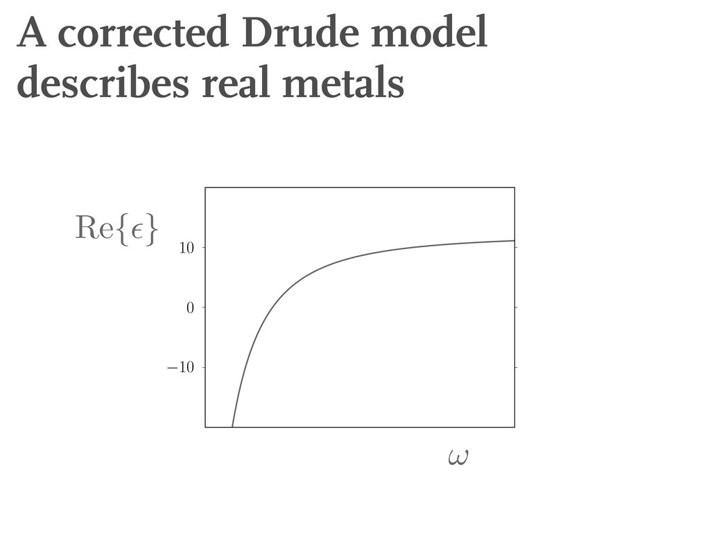
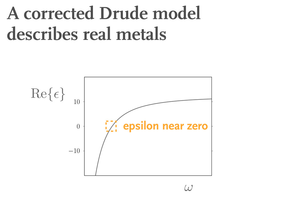
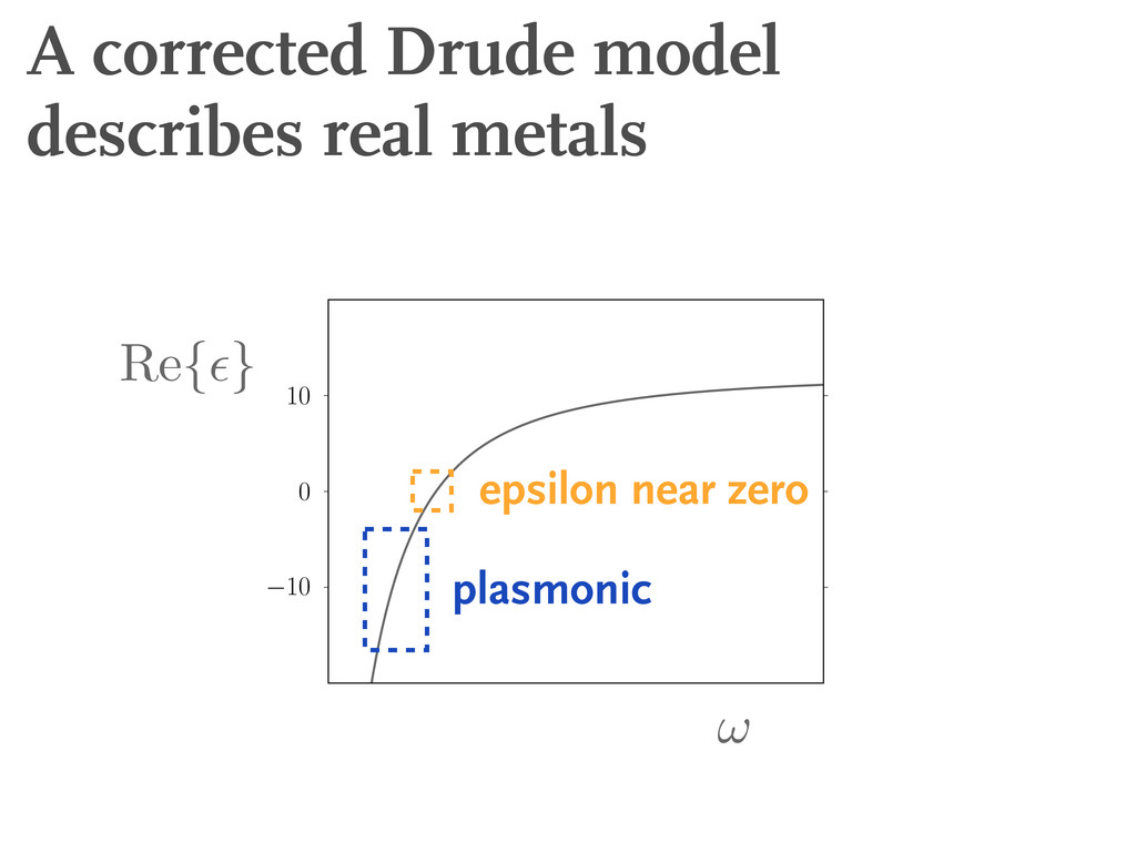
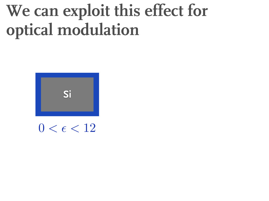
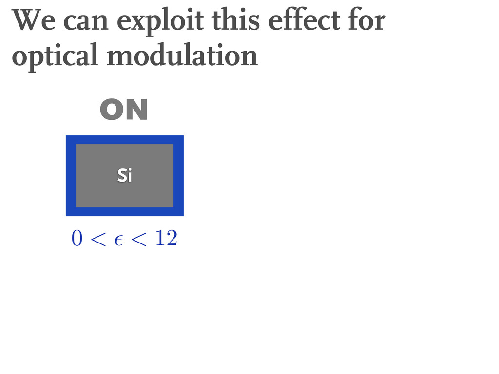
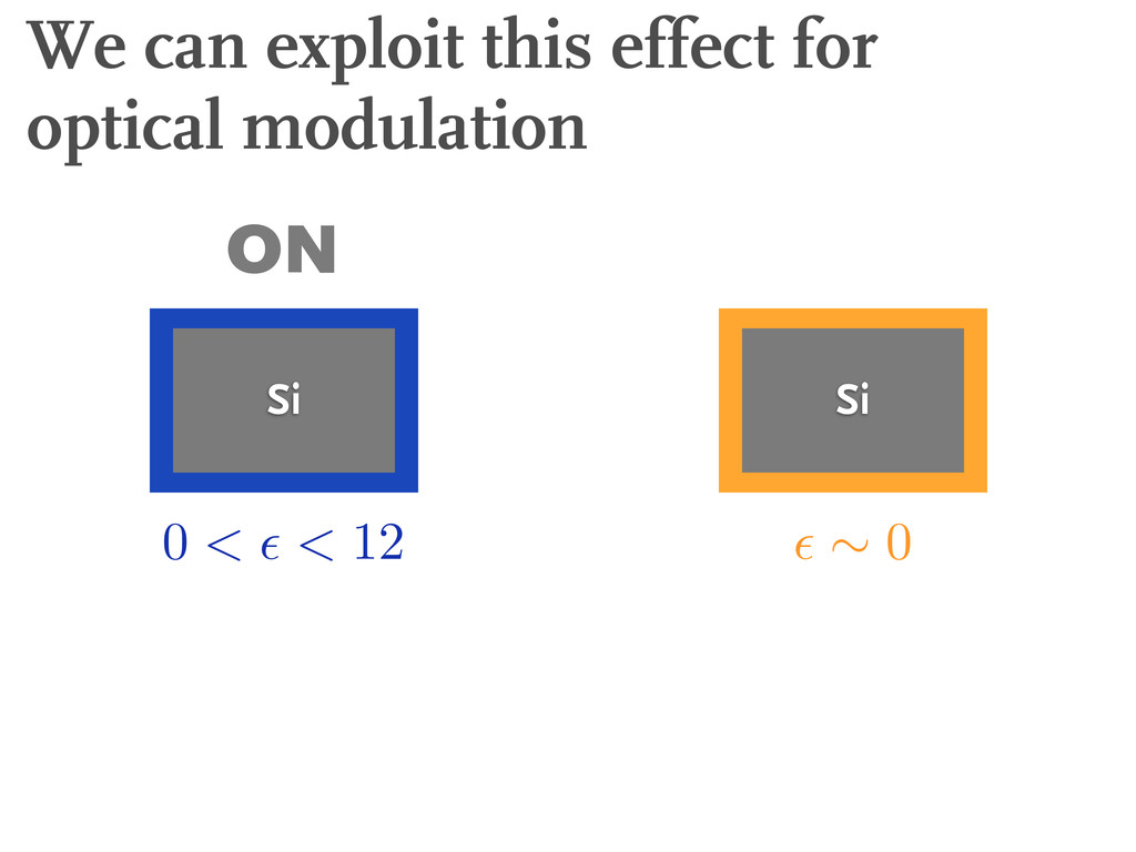
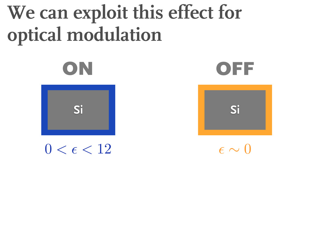
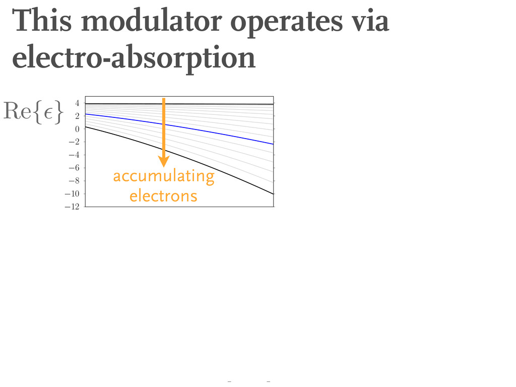
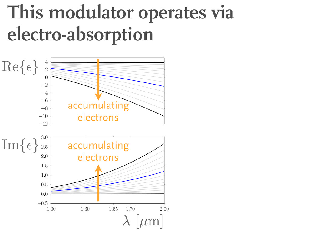
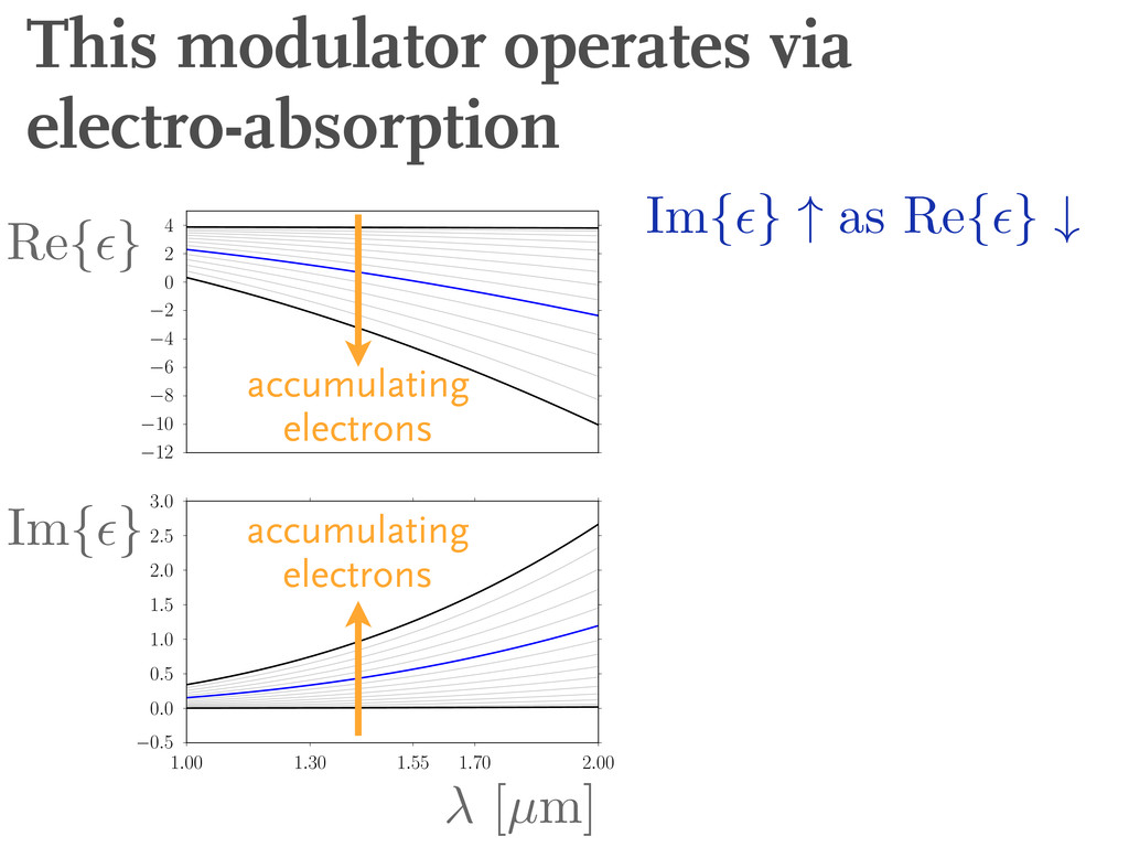
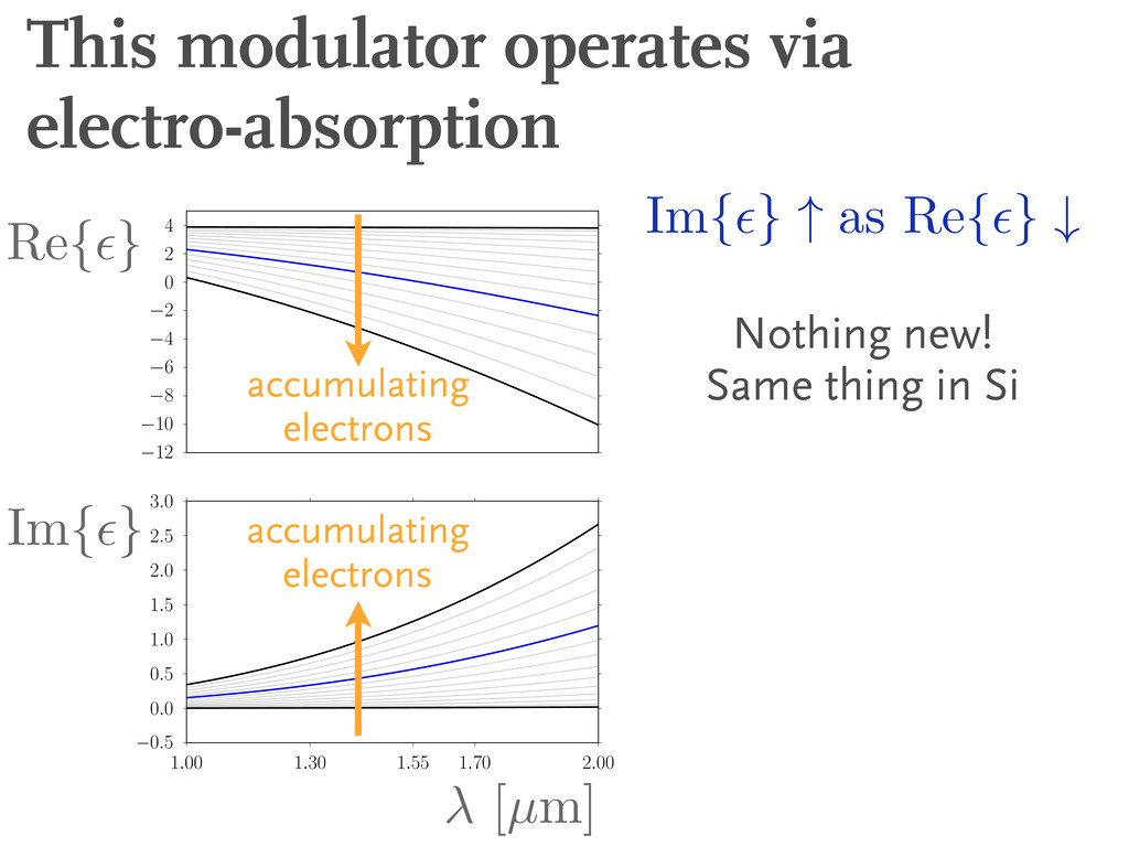
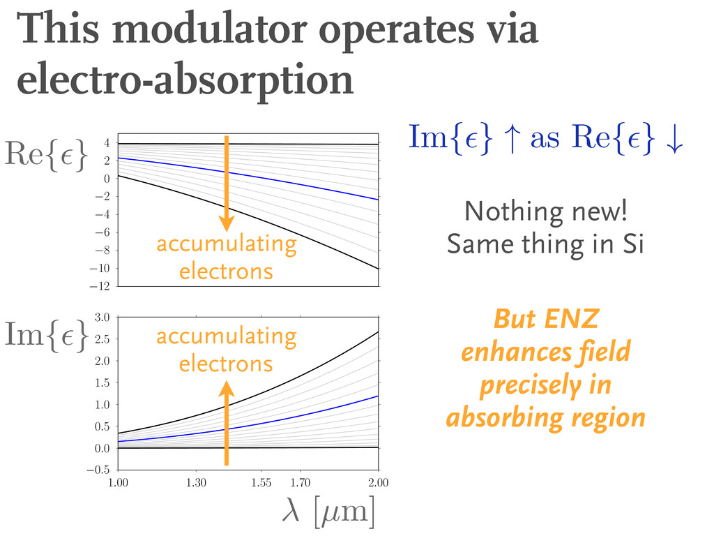
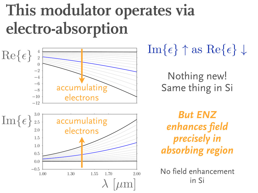
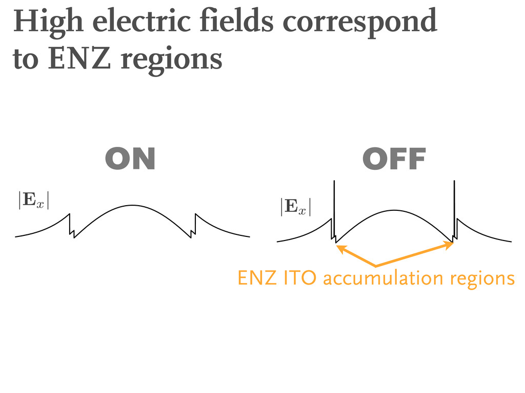
−2 0 2 4 1 1.00 1.30 1.55 1.70 2.00 Wavelength [µm] −0.5 0.0 0.5 1.0 1.5 2.0 2.5 3.0 2 _2{ } [µK] AK{ } accumulating electrons accumulating electrons AK{ } b _2{ } Nothing new! Same thing in Si But ENZ enhances field precisely in absorbing region No field enhancement in Si
![Epitaxial semiconductors and semimetals span the mid-IR Reflectance Wavelength [microns]](https://files.speakerdeck.com/presentations/5078727acd52500002012e6f/slide_43.jpg)