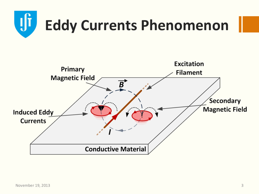
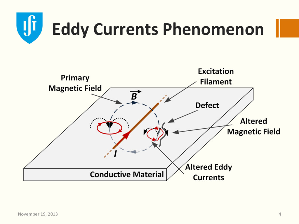
“Analysis techniques used in science and industry to evaluate the proper5es of a material, component or system without causing damage.” – Cartz, Louis (1995). Nondestruc0ve Tes0ng. A S M Interna0onal. – NDT techniques: • Ultrasonic; • Magne0c par0cles; • Radiographic; • Eddy currents… November 19, 2013 2
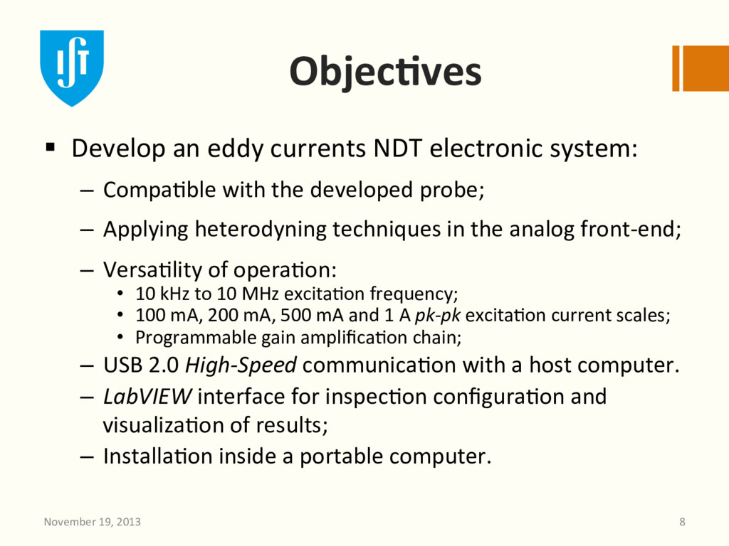
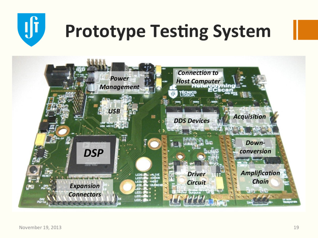
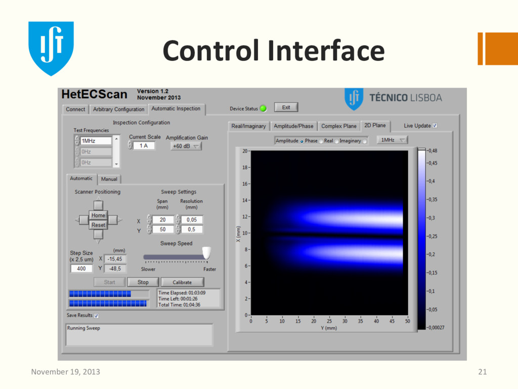
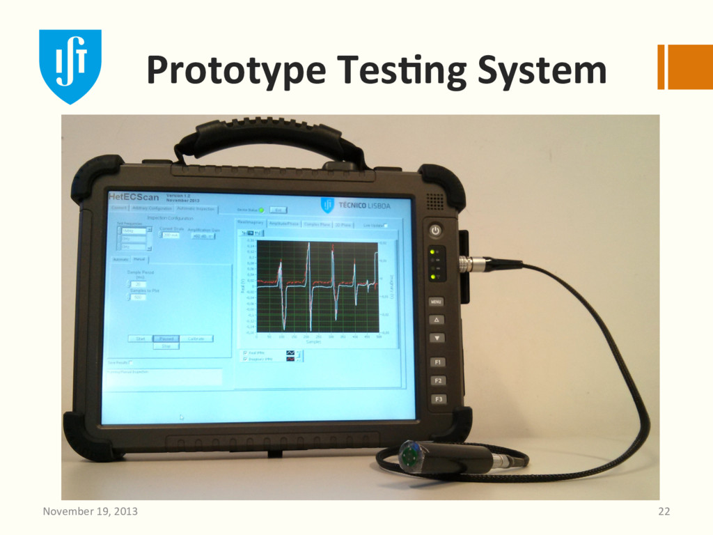
– Compa0ble with the developed probe; – Applying heterodyning techniques in the analog front-‐end; – Versa0lity of opera0on: • 10 kHz to 10 MHz excita0on frequency; • 100 mA, 200 mA, 500 mA and 1 A pk-‐pk excita0on current scales; • Programmable gain amplifica0on chain; – USB 2.0 High-‐Speed communica0on with a host computer. – LabVIEW interface for inspec0on configura0on and visualiza0on of results; – Installa0on inside a portable computer. November 19, 2013 8
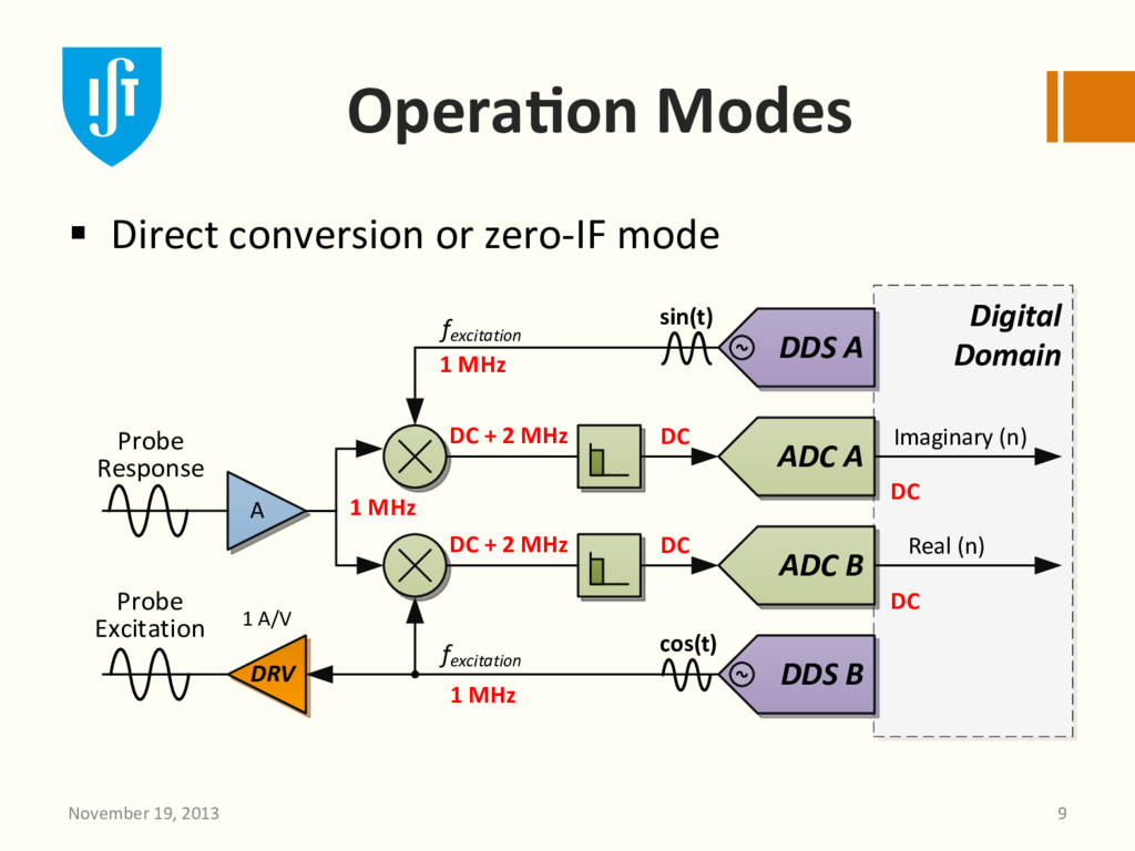
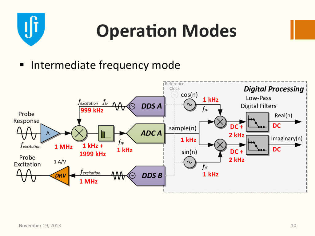
Imaginary (n) ADC B sin(t) DDS B DDS A DRV 1 A/V Probe Excitation fexcitation fexcitation Opera1on Modes § Direct conversion or zero-‐IF mode November 19, 2013 9 1 MHz 1 MHz 1 MHz DC + 2 MHz DC + 2 MHz DC DC DC DC
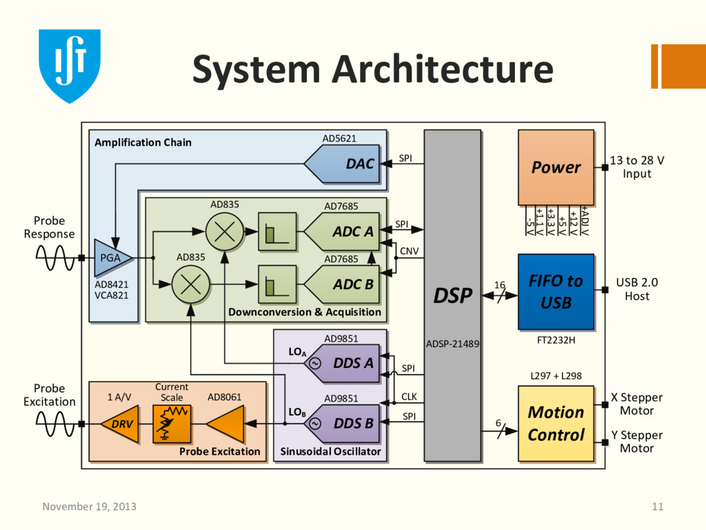
Chain Sinusoidal Oscillator Downconversion & Acquisition DSP ADC A PGA FIFO to USB Power Motion Control ADC B SPI DDS B DDS A DAC AD7685 AD7685 AD9851 AD835 AD835 AD5621 AD8421 VCA821 AD9851 Probe Excitation CNV 16 6 -5 V +1.1 V +3.3 V +5 V +12 V ADSP-21489 SPI SPI SPI CLK X Stepper Motor Y Stepper Motor USB 2.0 Host 13 to 28 V Input Probe Response FT2232H L297 + L298 LOA LOB +ADJ V DRV 1 A/V Current Scale AD8061 Probe Excitation
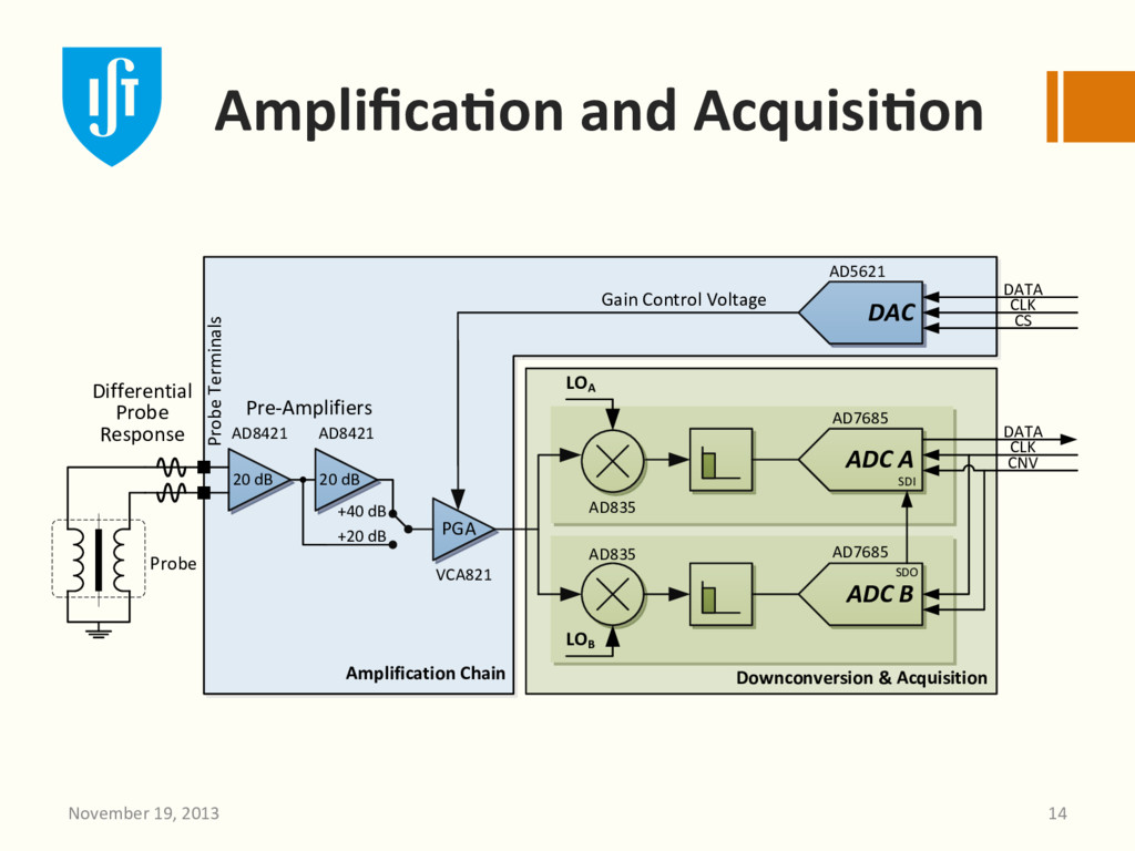
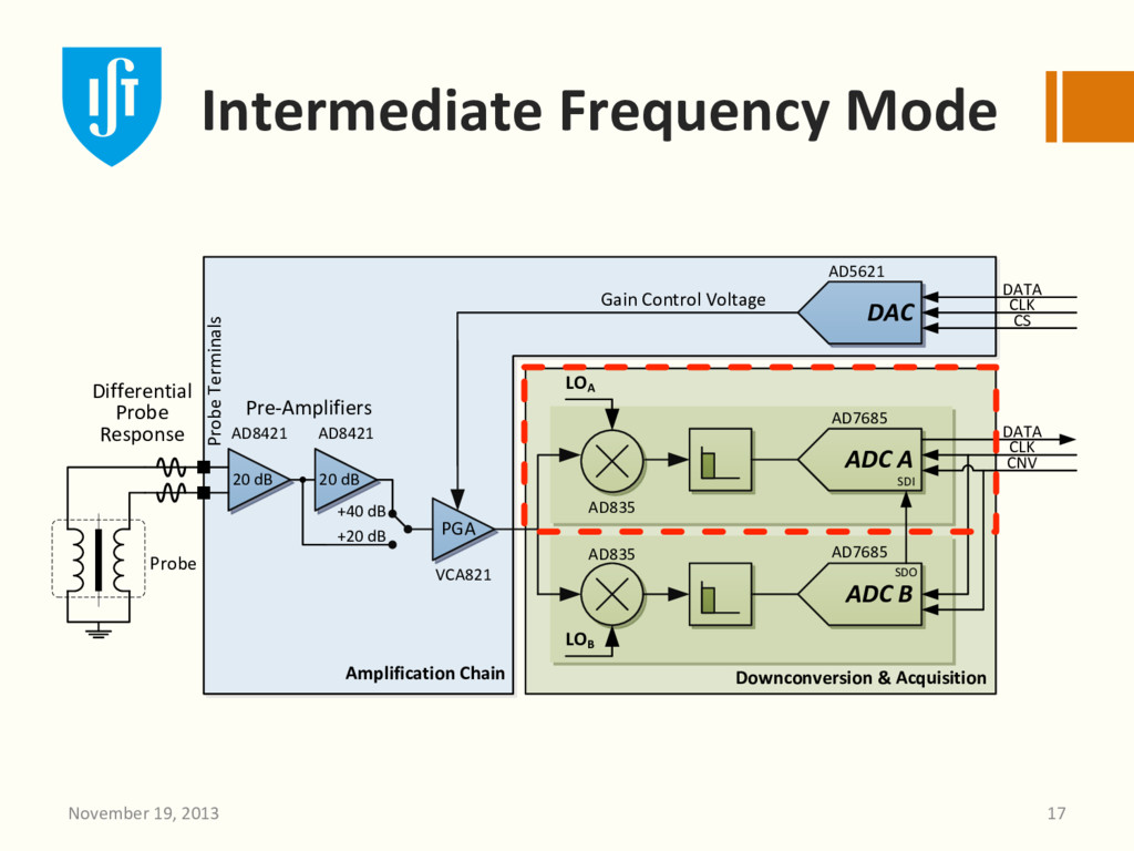
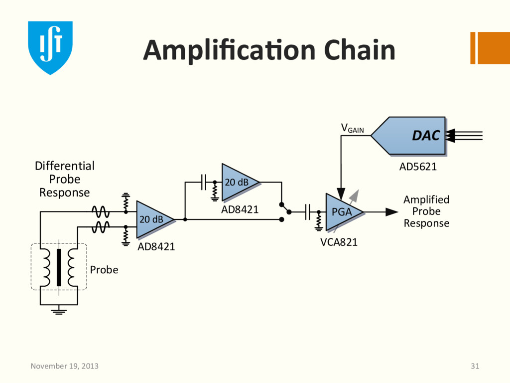
Amplification Chain Downconversion & Acquisition ADC A PGA ADC B DAC AD7685 AD7685 AD835 AD835 AD5621 Differential Probe Response Probe 20 dB 20 dB VCA821 AD8421 AD8421 LOA LOB SDO SDI DATA CLK CNV DATA CLK CS Probe Terminals Pre-Amplifiers Gain Control Voltage +20 dB +40 dB
Amplification Chain Downconversion & Acquisition ADC A PGA ADC B DAC AD7685 AD7685 AD835 AD835 AD5621 Differential Probe Response Probe 20 dB 20 dB VCA821 AD8421 AD8421 LOA LOB SDO SDI DATA CLK CNV DATA CLK CS Probe Terminals Pre-Amplifiers Gain Control Voltage +20 dB +40 dB
Amplification Chain Downconversion & Acquisition ADC A PGA ADC B DAC AD7685 AD7685 AD835 AD835 AD5621 Differential Probe Response Probe 20 dB 20 dB VCA821 AD8421 AD8421 LOA LOB SDO SDI DATA CLK CNV DATA CLK CS Probe Terminals Pre-Amplifiers Gain Control Voltage +20 dB +40 dB
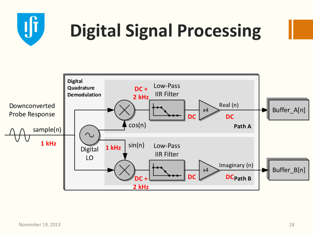
Digital Quadrature Demodulation Path A Path B x4 sample(n) Downconverted Probe Response x4 cos(n) sin(n) Digital LO Low-Pass IIR Filter Low-Pass IIR Filter Real (n) Imaginary (n) Buffer_B[n] Buffer_A[n] 1 kHz DC + 2 kHz DC 1 kHz DC DC + 2 kHz DC DC
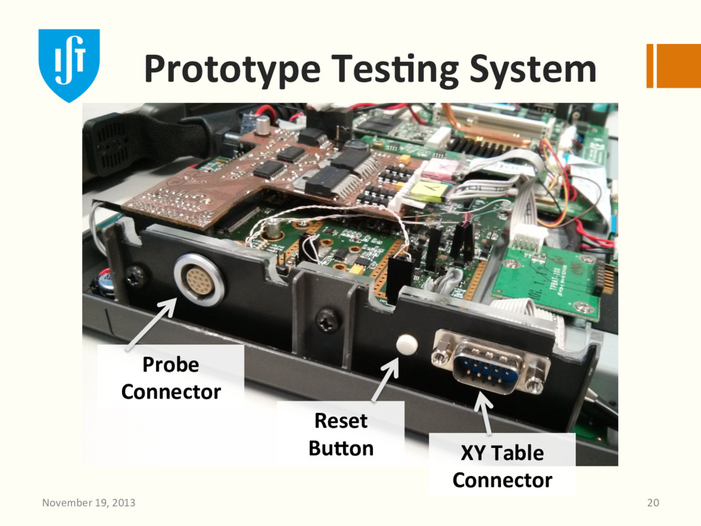
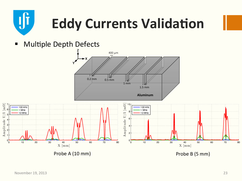
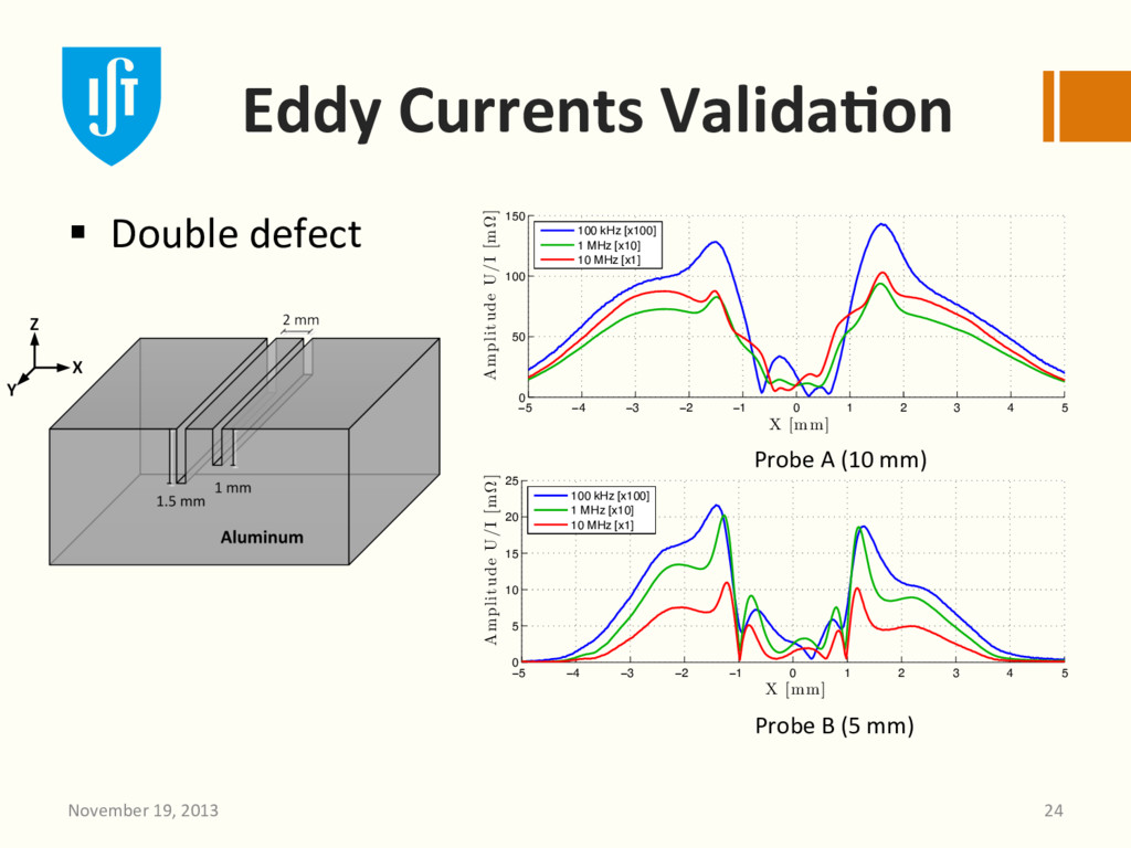
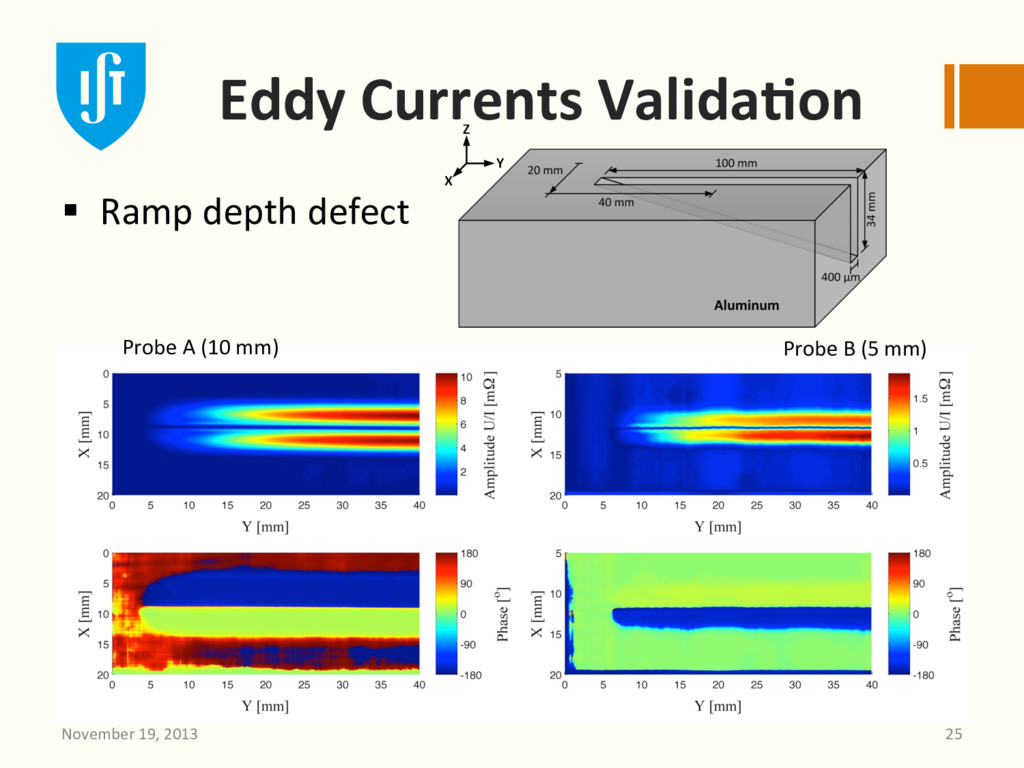
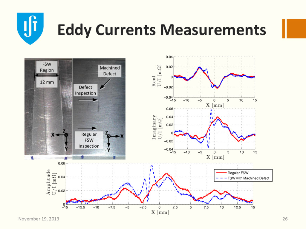
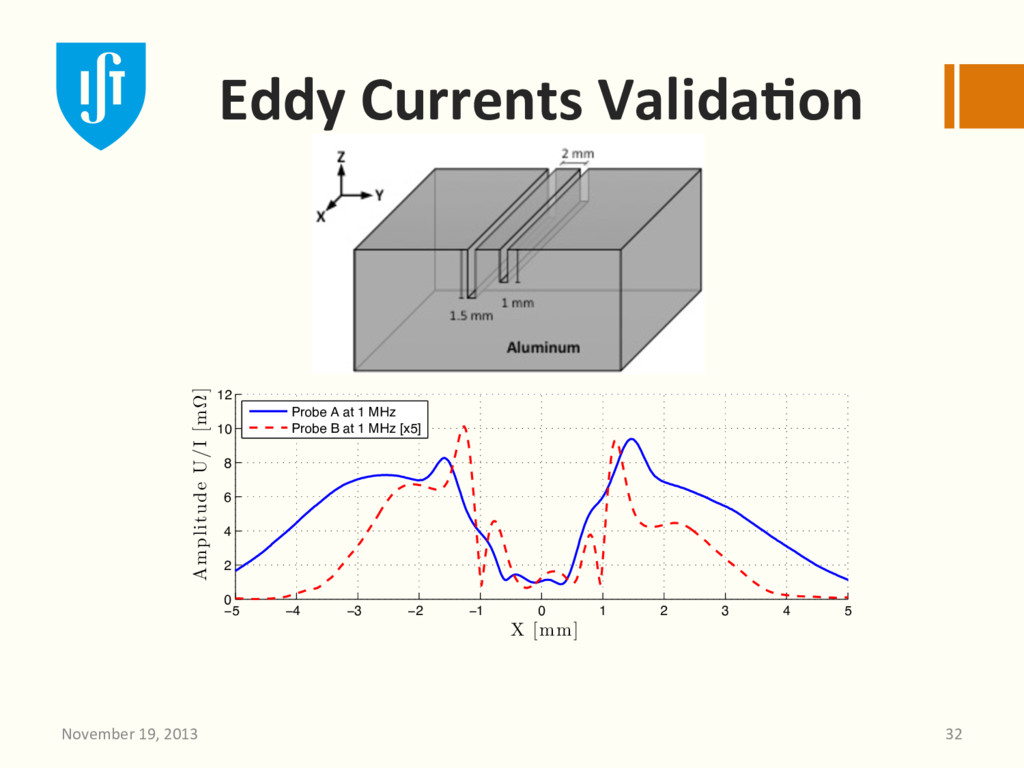
the reduc0on of system complexity. § The reduced system footprint allowed its installa0on inside a portable rugged computer, providing a standalone instrument. § The eddy currents NDT system was validated with the inspec0on of different machined defects. § FSW defects were also inspected successfully. Conclusions November 19, 2013 27
§ Op0mize the analog front-‐end for heterodyning direct conversion; § Develop a new mul0-‐channel NDT system; § Develop a system driver to allow the development of new host computer interfaces. Future Work November 19, 2013 28