Upgrade to Pro — share decks privately, control downloads, hide ads and more …

Impact of Defects on Solar Cell Performance in Selenium

Impact of Defects on Solar Cell Performance in Selenium

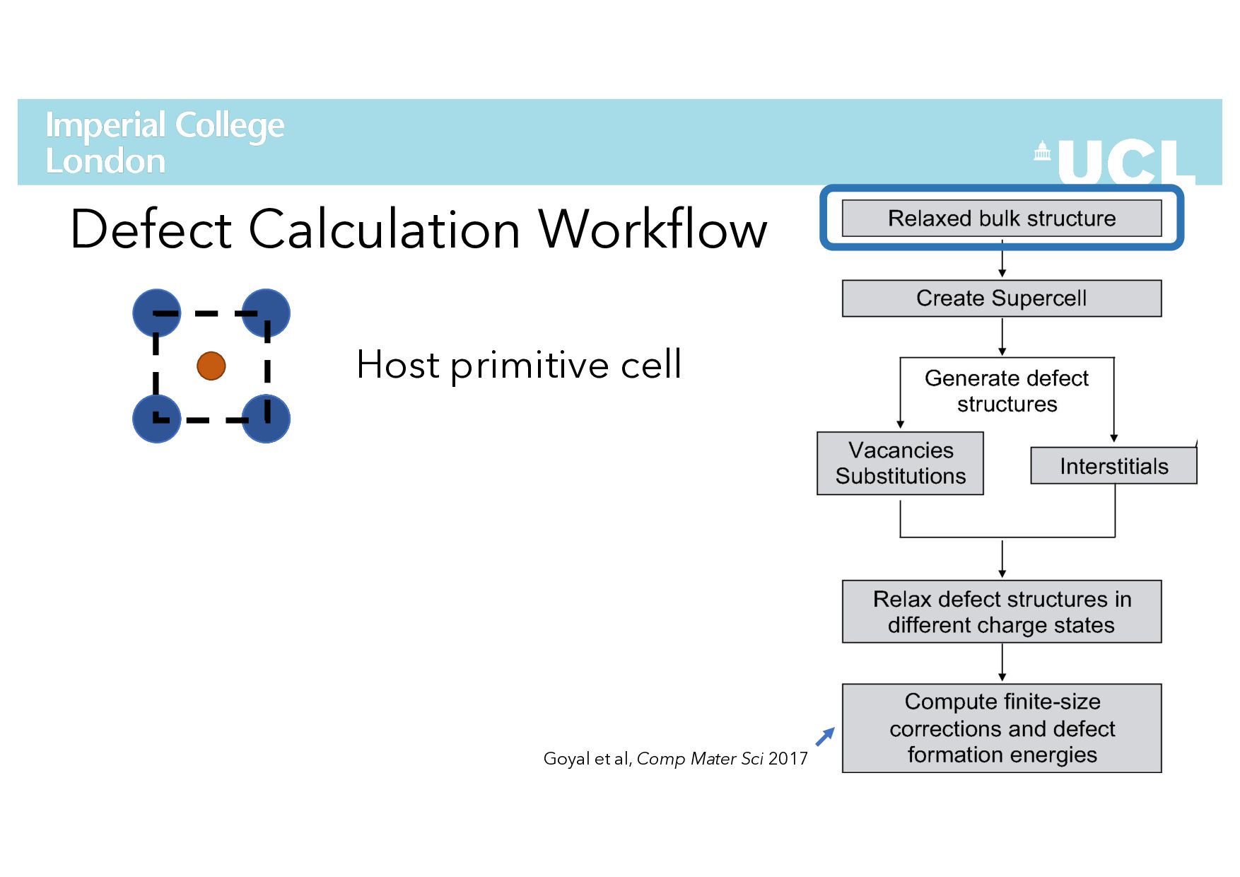
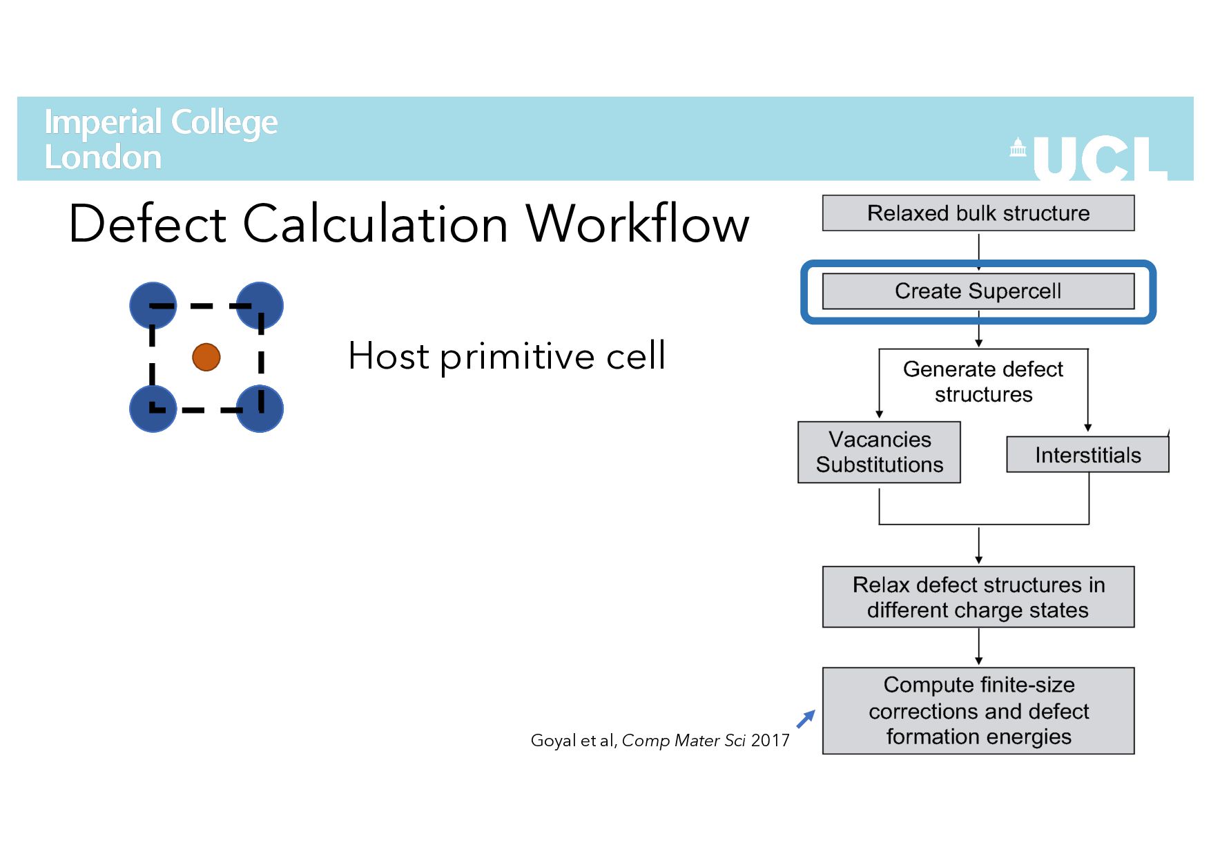
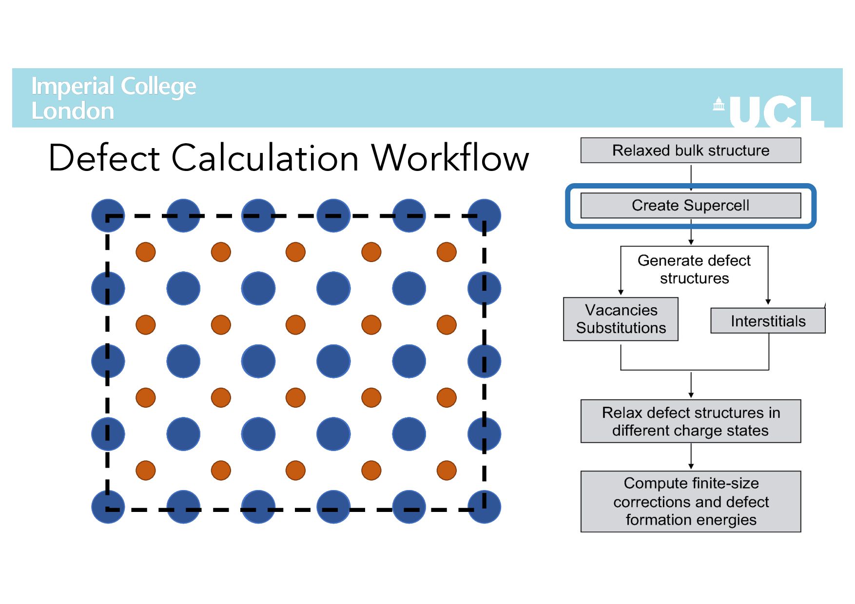
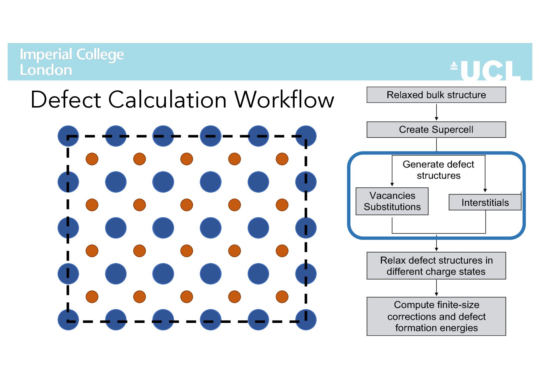
Slides for my talk on modelling defects in selenium and their impact on solar cell performance at MRS Spring 2023, San Francisco.

YouTube video recording: https://youtu.be/ZPobC2cS2KY

Hopefully a preprint on this work will be out soon! 🤞

References:
ShakeNBreak website: https://shakenbreak.readthedocs.io/en/latest/
Our general defect calculation package doped is available here: https://github.com/SMTG-UCL/doped

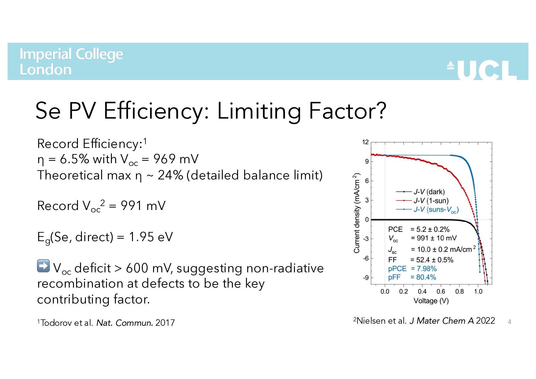
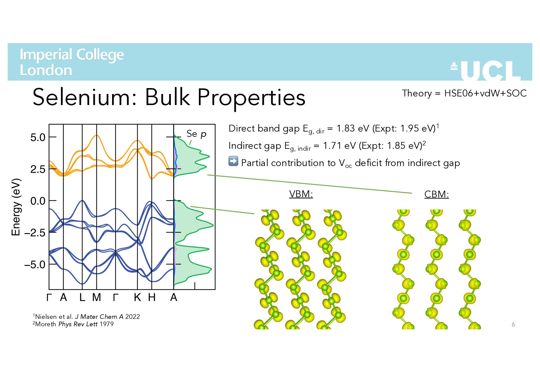
See the referenced paper from Rasmus Nielsen on Se solar cells here: https://doi.org/10.1039/D2TA07729A

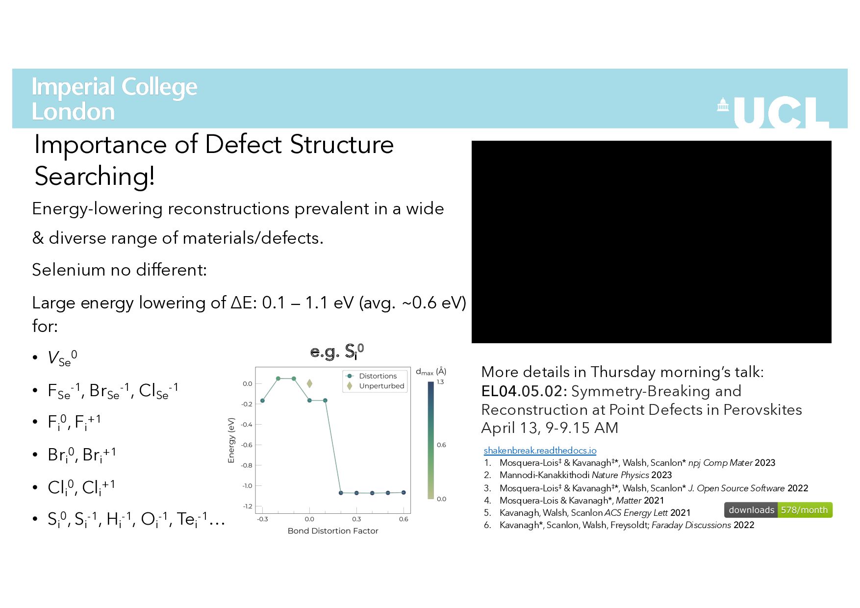
See our open-access papers on defect structure-searching here:
https://www.nature.com/articles/s41524-023-00973-1
https://joss.theoj.org/papers/10.21105/joss.04817
https://www.nature.com/articles/s41567-023-02049-9

Questions welcome! For other computational photovoltaics, defects and disorder talks, have a look at my YouTube channel!
https://www.youtube.com/SeanRKavanagh
For other research articles see:
https://bit.ly/3pBMxOG

Seán R. Kavanagh

May 02, 2023
Tweet

More Decks by Seán R. Kavanagh

Other Decks in Research

Transcript

  1. 1
    02/05/2023
    Impact of Defects on Solar Cell
    Performance in Selenium
    Seán Kavanagh
    Profs: David O. Scanlon & Aron Walsh
    [email protected]
    (University College London & Imperial College London) Y.-T. Huang, S. R. Kavanagh, D.O. Scanlon, A. Walsh,
    R.L.Z. Hoye, Nanotechnology 32, 132004 (2021)

    View Slide

  2. 2
    02/05/2023
    Impact of Defects on Solar Cell
    Performance in Selenium
    Seán Kavanagh
    Profs: David O. Scanlon & Aron Walsh
    [email protected]
    (University College London & Imperial College London) Y.-T. Huang, S. R. Kavanagh, D.O. Scanlon, A. Walsh,
    R.L.Z. Hoye, Nanotechnology 32, 132004 (2021)

    View Slide

  3. Why Selenium?
    • First material used for photovoltaic (PV) solar cells, in 1883 (η < 1%).
    • Researchers then moved on to c-Si, CdTe, CZTS/CIGS, perovskites...
    • Recent surge in interest after decades of neglect, following Todorov
    et al. record efficiency η = 6.5% in 2017.
    • Low-temperature solution-growth & processing, “simple” chemistry,
    chain-like structure could yield benign grain boundaries.
    • Wide-bandgap (~1.9 eV) suitable for single-junction or tandem PV.
    3

    View Slide

  4. Se PV Efficiency: Limiting Factor?
    4
    2Nielsen et al. J Mater Chem A 2022
    Record Efficiency:1
    η = 6.5% with Voc
    = 969 mV
    Theoretical max η ~ 24% (detailed balance limit)
    Record Voc
    2 = 991 mV
    Eg
    (Se, direct) = 1.95 eV
    ➡ Voc
    deficit > 600 mV, suggesting non-radiative
    recombination at defects to be the key
    contributing factor.
    1Todorov et al. Nat. Commun. 2017

    View Slide

  5. Selenium: Bulk Properties
    5
    Strong inter-chain vdW
    dispersion interactions
    ~10% volume decrease when
    including vdW effects
    Theory (Hybrid DFT
    + vdW)
    Experiment
    Direction a,b c a,b c
    Lattice Parameter (Å) 4.34 4.96 4.37 4.95
    Volume (Å3) 81.1 81.9
    εionic
    0.63 0.94 0.461 0.621
    ε∞ (optical)
    6.71 10.28 6.971 11.621
    Esurface
    (J/m2) 0.18 0.1752
    1Danielewicz & Coleman Appl. Opt, 1974
    210.1016/0022-3093(71)90004-4

    View Slide

  6. Selenium: Bulk Properties
    6
    Se p
    Direct band gap Eg, dir
    = 1.83 eV (Expt: 1.95 eV)1
    Indirect gap Eg, indir
    = 1.71 eV (Expt: 1.85 eV)2
    ➡ Partial contribution to Voc
    deficit from indirect gap
    1Nielsen et al. J Mater Chem A 2022
    2Moreth Phys Rev Lett 1979
    CBM:
    VBM:
    Theory = HSE06+vdW+SOC

    View Slide

  7. Defect Calculation Workflow
    7
    Host primitive cell
    Goyal et al, Comp Mater Sci 2017

    View Slide

  8. Defect Calculation Workflow
    8
    Host primitive cell
    Goyal et al, Comp Mater Sci 2017

    View Slide

  9. Defect Calculation Workflow
    9

    View Slide

  10. Defect Calculation Workflow
    10

    View Slide

  11. Defect Calculation Workflow
    11

    View Slide

  12. Defect Calculation Workflow
    12

    View Slide

  13. Defect Calculation Workflow
    13

    View Slide

  14. Defect Calculation Workflow
    14

    View Slide

  15. Defect Calculation Workflow
    15
    ➡ Energy
    ➡ Concentration
    ➡ Transition Level
    ➡ Deep/Shallow
    ➡ Doping
    ➡ Carrier capture
    ➡ Diffusion
    ➡ …

    View Slide

  16. Computational Defect Thermodynamics
    VBM CBM
    D+1
    D0
    D-1
    Fermi Level E
    F
    (eV)
    Formation Energy ΔH
    X,q
    (eV)
    ε(+1/0) ε(0/-1)
    E
    F
    VBM
    CBM
    ε(+1/0)
    ε(0/-1)
    Kavanagh*, Scanlon, Walsh, Freysoldt Faraday Discussions 2022

    View Slide

  17. Intrinsic Defect Formation Energy Diagram
    17
    Sei
    0 = Dominant, lowest energy native defect
    • Electrically benign
    • Neutral across most of the bandgap, with a
    negative-U (0/-2) level just below the CBM.
    0
    -1
    -2
    0
    -2
    +1
    Calculated with doped (GitHub.com/SMTG-UCL/doped)
    & ShakeNBreak (shakenbreak.readthedocs.io), using VASP

    View Slide

  18. Why is Sei
    0 so low energy?
    Split-interstitial motif:
    Sei
    0 joins Se chain which
    twists to accommodate.
    ➡ Low-energy & no
    dangling bonds
    -> stays neutral.
    18

    View Slide

  19. Intrinsic Defect Formation Energy Diagram
    19
    0
    -1
    -2
    0
    -2
    +1
    Calculated with doped (GitHub.com/SMTG-UCL/doped)
    & ShakeNBreak (shakenbreak.readthedocs.io), using VASP
    VSe
    (0/-1)
    VSe
    (+1/0)
    VSe
    (-1/-2)
    VSe
    -> Moderate formation energy, expect
    low but non-negligible concentrations.
    • Multiple in-gap defect levels, which could
    be active for carrier recombination.

    View Slide

  20. Vacancy Defects (VSe
    )
    +1:
    Terminated +
    Bridging Chain
    0* (ΔE = 27 meV):
    ‘Self-healed’
    Chain
    0 and -1:
    Two Terminated
    Chains
    -2:
    Elongated Bonds; ‘Self-
    healed’ + Bridging

    View Slide

  21. Intrinsic Defect Formation Energy Diagram
    21
    0
    -1
    -2
    0
    -2
    +1
    Calculated with py-sc-fermi
    = EF
    Anneal Temperature = 300K
    Fermi level (EF
    ) determined by charge neutrality condition: p + ND
    + = n + NA

    View Slide

  22. 22
    0
    -1
    -2
    0
    -2
    +1
    = EF
    Intrinsic Defect Formation Energy Diagram
    Anneal Temperature = 463 K (190℃)
    Calculated with py-sc-fermi
    Fermi level (EF
    ) determined by charge neutrality condition: p + ND
    + = n + NA

    View Slide

  23. 23
    0
    -1
    -2
    0
    -2
    +1
    = EF
    Intrinsic Defect Formation Energy Diagram
    Anneal Temperature = 1000K
    Calculated with py-sc-fermi
    Fermi level (EF
    ) determined by charge neutrality condition: p + ND
    + = n + NA

    View Slide

  24. 24
    • Se without impurities -> insulating/weakly p-type
    • Large p-type doping window
    • High sensitivity to p-type impurities
    • n-type doping not possible
    • But experiment1 sees ~1016 holes/cm-3…
    1Nielsen et al. J Mater Chem A 2022
    0
    -1
    -2
    0
    -2
    +1
    Calculated with doped (GitHub.com/SMTG-UCL/doped)
    & ShakeNBreak (shakenbreak.readthedocs.io), using VASP
    = EF
    Sei
    VSe
    Anneal Temperature = 463 K (190℃)

    View Slide

  25. What Else is In There?
    Potential impurities:
    • Halogens are common impurities in chalcogenide materials, often
    present in supplier precursors ➡ F, Cl, Br
    • Typically grown on Tellurium substrates ➡ Te
    • Typically annealed in air to aid crystallization ➡ O
    • Hydrogen is a very common impurity in materials ➡ H
    • Sulfur present in precursors, can bond easily with Se ➡ S
    25
    • Experiment1 sees ~1016 holes/cm-3…
    • Not from intrinsic defects

    View Slide

  26. 26
    Substitutions: XSe
    Interstitials: Xi
    F
    Cl
    Br
    H
    O
    S
    Te
    Calculated with doped (GitHub.com/SMTG-UCL/doped)
    & ShakeNBreak (shakenbreak.readthedocs.io) Using dopant-rich chemical potential limits
    Halogens
    Chalcogens
    Hydrogen

    View Slide

  27. VSe
    +1:
    Terminated +
    Bridging Chain
    Stable Positive Halogen Interstitials?
    Fi
    +1:
    Two Bridging Chains
    + Se-F Bond
    Fi
    -1:
    Intercalated F-1 ion

    View Slide

  28. Energy-lowering reconstructions prevalent in a wide
    & diverse range of materials/defects.
    Selenium no different:
    Large energy lowering of ΔE: 0.1 – 1.1 eV (avg. ~0.6 eV)
    for:
    • VSe
    0
    • FSe
    -1, BrSe
    -1, ClSe
    -1
    • Fi
    0, Fi
    +1
    • Bri
    0, Bri
    +1
    • Cli
    0, Cli
    +1
    • Si
    0, Si
    -1, Hi
    -1, Oi
    -1, Tei
    -1… 28
    e.g. Si
    0
    Importance of Defect Structure
    Searching!
    More details in Thursday morning’s talk:
    EL04.05.02: Symmetry-Breaking and
    Reconstruction at Point Defects in Perovskites
    April 13, 9-9.15 AM
    shakenbreak.readthedocs.io
    1. Mosquera-Lois‡ & Kavanagh‡*, Walsh, Scanlon* npj Comp Mater 2023
    2. Mannodi-Kanakkithodi Nature Physics 2023
    3. Mosquera-Lois‡ & Kavanagh‡*, Walsh, Scanlon* J. Open Source Software 2022
    4. Mosquera-Lois & Kavanagh*, Matter 2021
    5. Kavanagh, Walsh, Scanlon ACS Energy Lett 2021
    6. Kavanagh*, Scanlon, Walsh, Freysoldt; Faraday Discussions 2022

    View Slide

  29. 0.0 0.8 1.6
    Fermi Level (eV)
    0.0
    0.5
    1.0
    1.5
    Formation Energy (eV)
    Sei
    VSe
    Fi
    29
    • Fluorine interstitials could increase hole
    concentrations slightly, but still <1013 cm-3
    • Experiment sees ~1016 holes/cm-3…
    Calculated with doped (GitHub.com/SMTG-UCL/doped)
    & ShakeNBreak (shakenbreak.readthedocs.io), using VASP
    = EF
    Anneal Temperature = 463 K (190℃)
    0.0
    0.5
    1.0
    1.5 Sei
    VSe
    Fi

    View Slide

  30. Conclusions & Future Steps
    • Self-interstitials are neutral and benign for recombination, but Se
    vacancies could capture charge carriers.
    • ➡ Explicitly calculate non-radiative recombination rates of Vse
    • ➡ Devise passivation strategies; out-of-equilibrium Se over-pressures? Fermi
    level control during growth/annealing?
    • Hydrogen/halogens/chalcogens do not seem to be the cause of p-
    type doping in Selenium. Se chains show strong valence alternation
    & re-bonding to self-compensate.
    • ➡ Pnictogens (N, P, As) perhaps? Chalcogen substitutions are low energy,
    pnictogens could also substitute and be under-valent (-> negatively-charged)
    30

    View Slide

  31. Acknowledgements
    31
    @Kavanagh_Sean_
    [email protected]
    Rasmus Nielsen @ DTU Physics
    -> Growing & characterizing
    Selenium thin-films for PV
    Talk Friday morning:
    EN04.14.02: The Renaissance
    of Selenium Thin-Film Solar
    Cells; April 14, 8.45-9 AM
    Profs David Scanlon & Aron Walsh
    Alp Samli
    Intrinsic:

    View Slide

  32. Other Results:
    Band Alignment
    Lower VBM compared
    to Sb2
    Se3
    as expected
    (anti-bonding Sb s – Se
    p interaction in Sb2
    Se3
    gives raised VBM)
    32

    View Slide

  33. Other results:
    • Interestingly, PBEsol seems to perform terribly for this material, with or
    without D3 vdW dispersion correction. Gives lattice parameter errors
    ~8%, HSE06-on-PBEsol structure gives a bandgap underestimated by
    50% compared to HSE06-on-HSE06 or experiment, and the ionic
    dielectric is off by an order of magnitude (again compared to HSE06 or
    experiment which match) due to the severely underestimated interchain
    distances (which makes a big difference to inter-chain interactions)
    • PBE does better, but still not great (checked against Materials Project
    PBE results). Errors of around 3-4% in the lattice parameters both with
    and without D3 (overestimates a,b without D3, underestimates with D3).
    • Dispersion-corrected hybrid DFT (HSE06+D3) is very accurate for the
    bulk properties of Se on the other hand; gives lattice parameters
    matching experiment to 1%, closely matches the experimental bandgap
    (ΔEg
    <0.1 eV), matches the experimental dielectric screening (both ionic
    and electronic contributions) very well…
    33

    View Slide