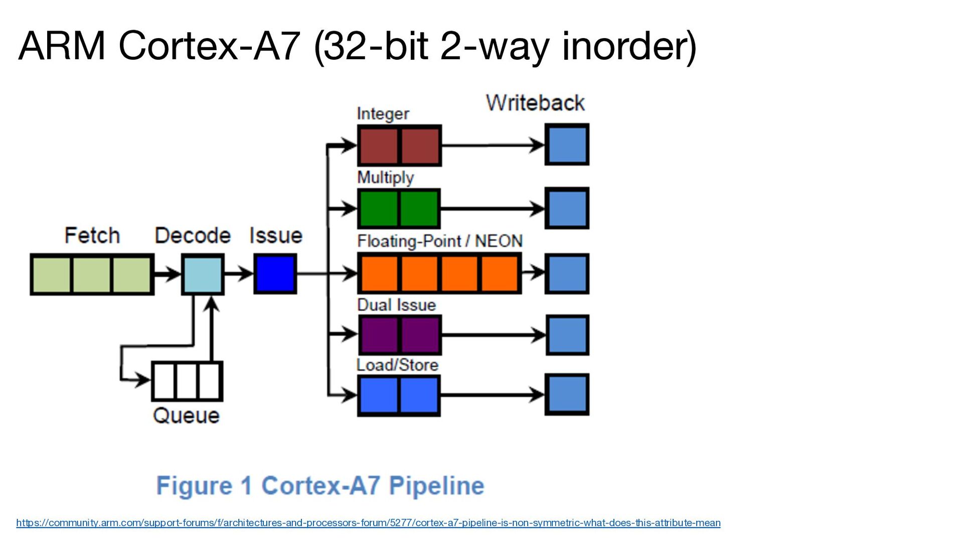
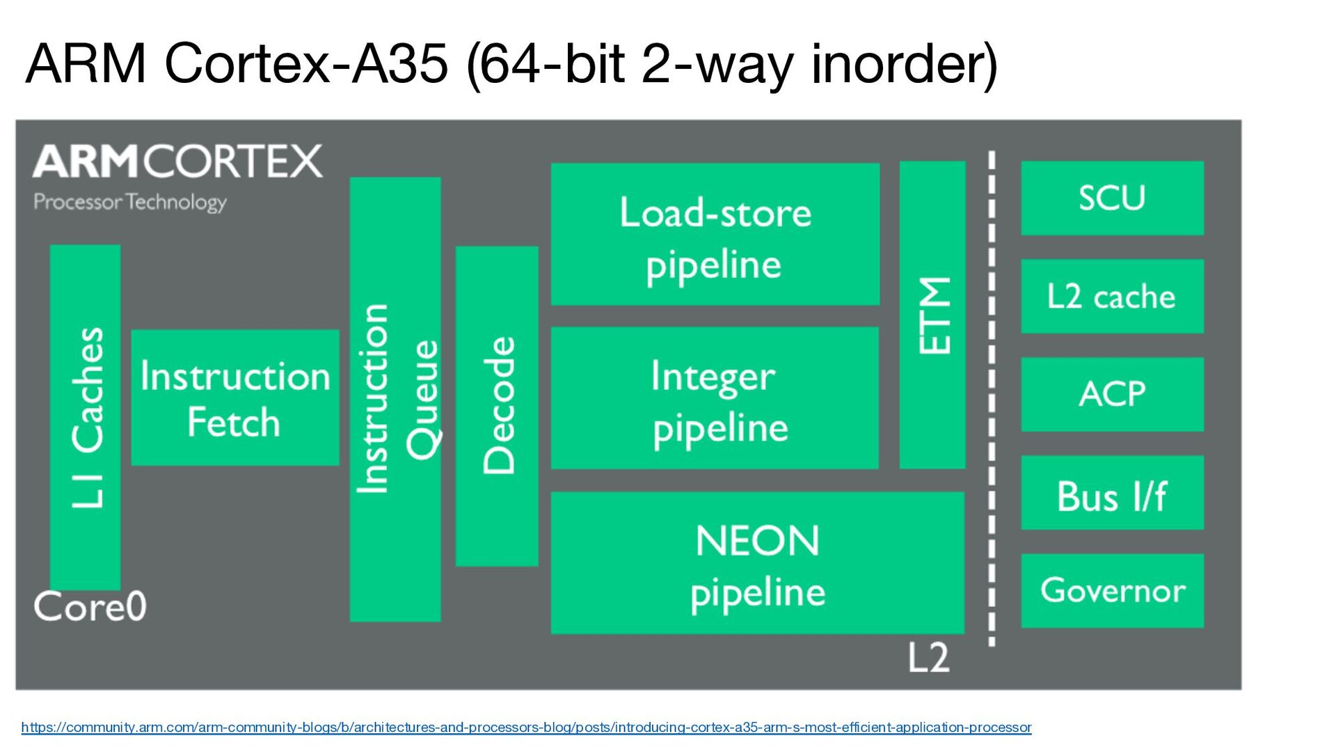
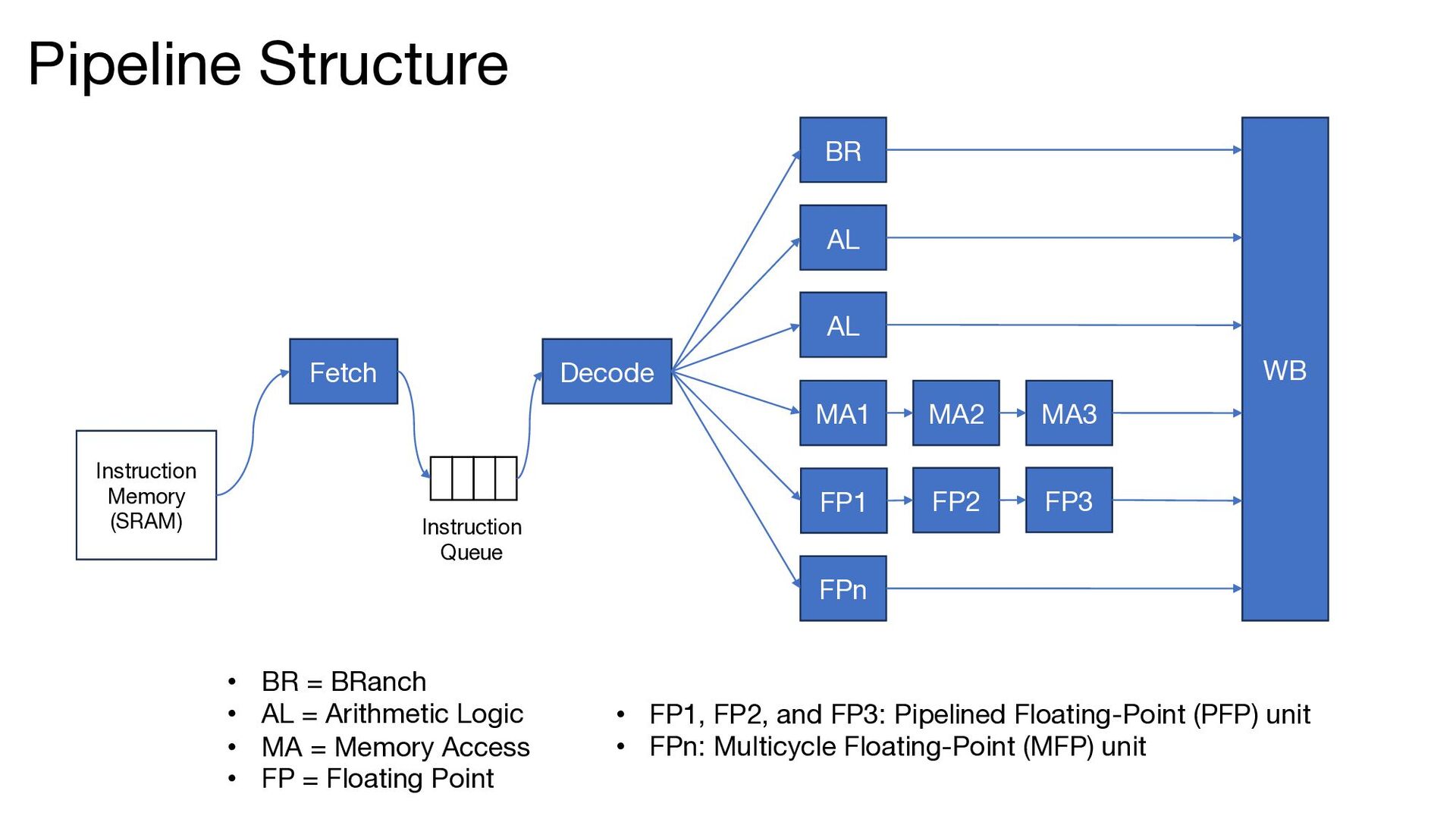
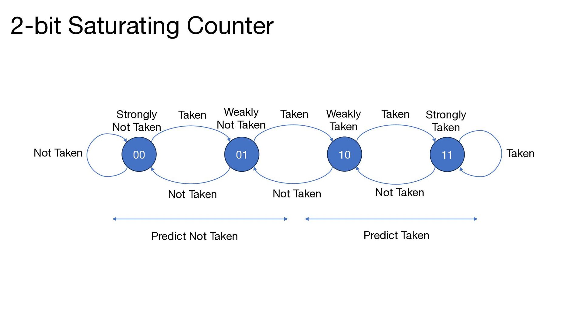
The ISA is based on RISC-V • The microarchitecture was inspired by the ARM Cortex-A series • The CPU includes the following features: • Two-way in-order superscalar architecture • GShare branch predictor • Early branch resolution
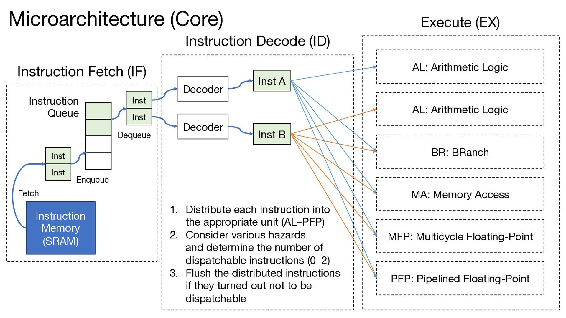
(IF) Instruction Decode (ID) Inst A Inst B Execute (EX) AL: Arithmetic Logic AL: Arithmetic Logic BR: BRanch MA: Memory Access MFP: Multicycle Floating-Point PFP: Pipelined Floating-Point 1. Distribute each instruction into the appropriate unit (AL–PFP) 2. Consider various hazards and determine the number of dispatchable instructions (0–2) 3. Flush the distributed instructions if they turned out not to be dispatchable Instruction Memory (SRAM) Fetch Decoder Decoder Microarchitecture (Core)
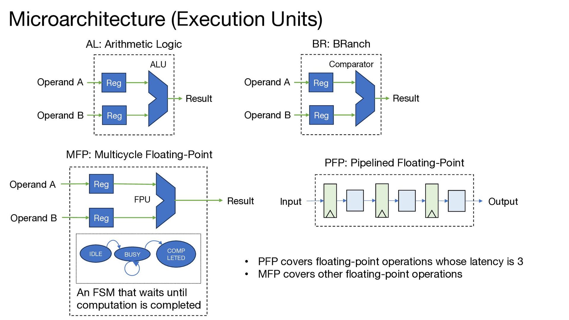
(Execution Units) Reg Reg Operand A Operand B Result ALU BR: BRanch Reg Reg Operand A Operand B Result Comparator Reg Reg Operand A Operand B Result FPU IDLE COMP LETED BUSY An FSM that waits until computation is completed Input Output • PFP covers floating-point operations whose latency is 3 • MFP covers other floating-point operations
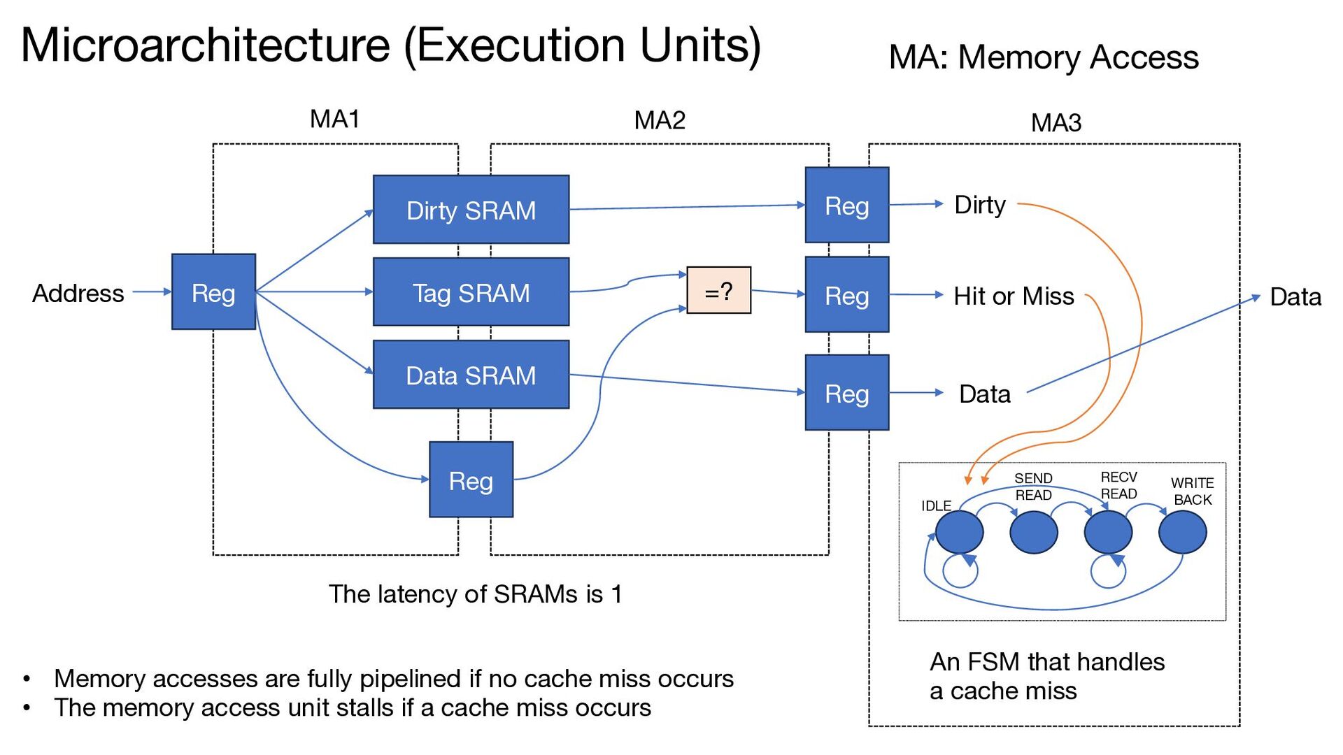
Address Reg =? Hit or Miss Reg Reg Data Reg Dirty MA1 MA2 MA3 IDLE SEND READ RECV READ WRITE BACK An FSM that handles a cache miss Data The latency of SRAMs is 1 MA: Memory Access • Memory accesses are fully pipelined if no cache miss occurs • The memory access unit stalls if a cache miss occurs
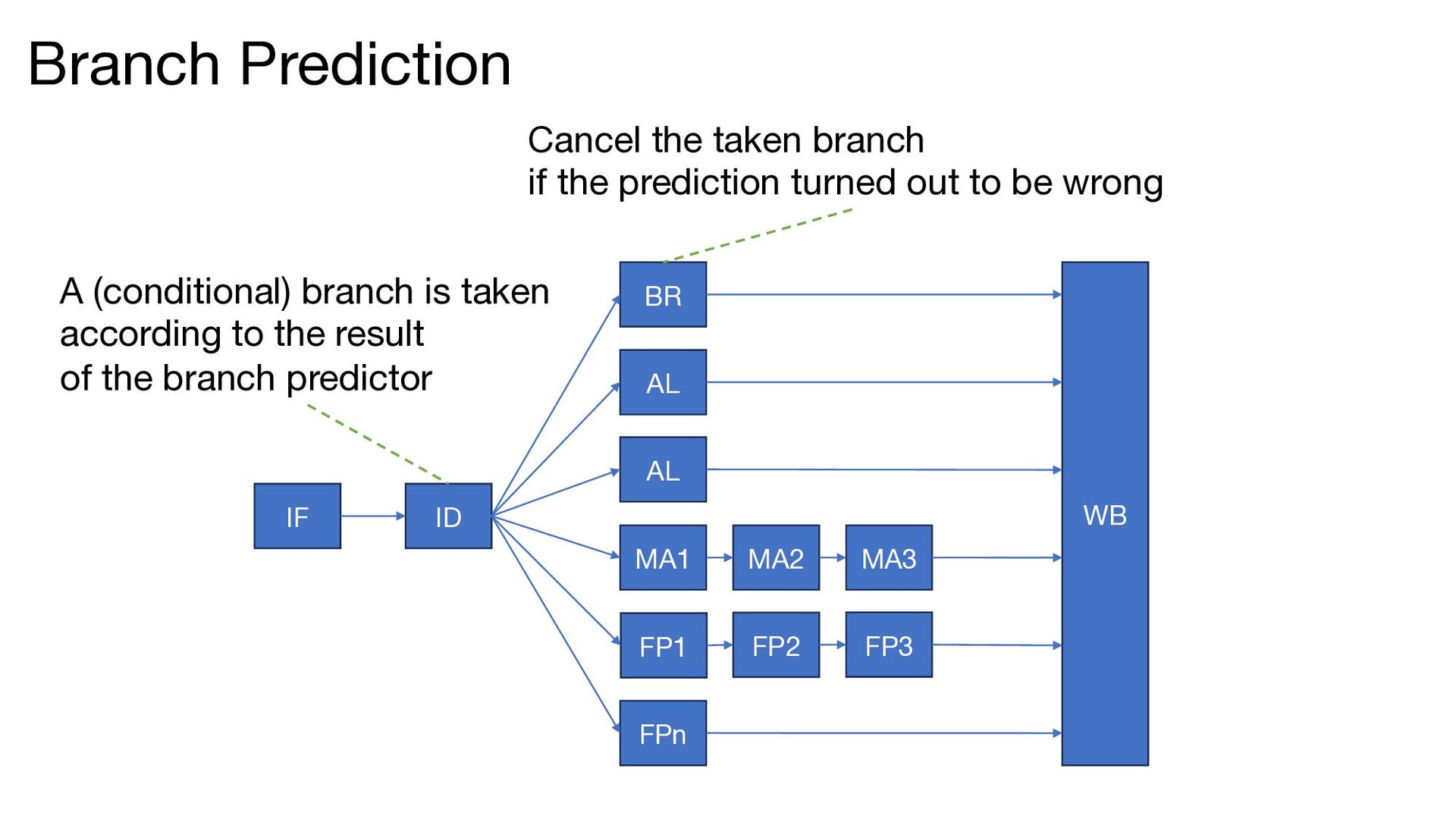
FP2 FP3 WB Branch Prediction A (conditional) branch is taken according to the result of the branch predictor Cancel the taken branch if the prediction turned out to be wrong
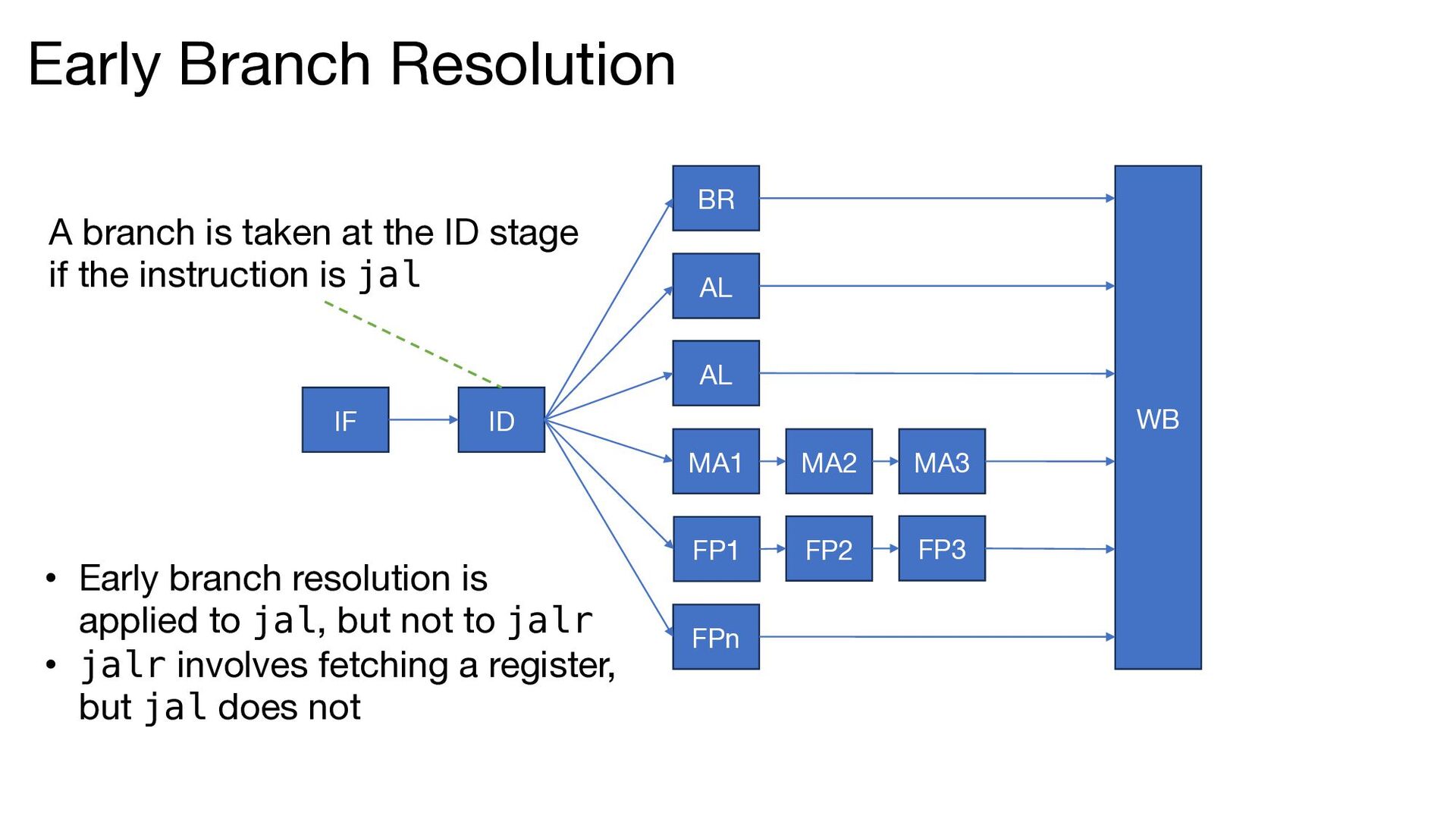
FP2 FP3 WB Early Branch Resolution A branch is taken at the ID stage if the instruction is jal • Early branch resolution is applied to jal, but not to jalr • jalr involves fetching a register, but jal does not
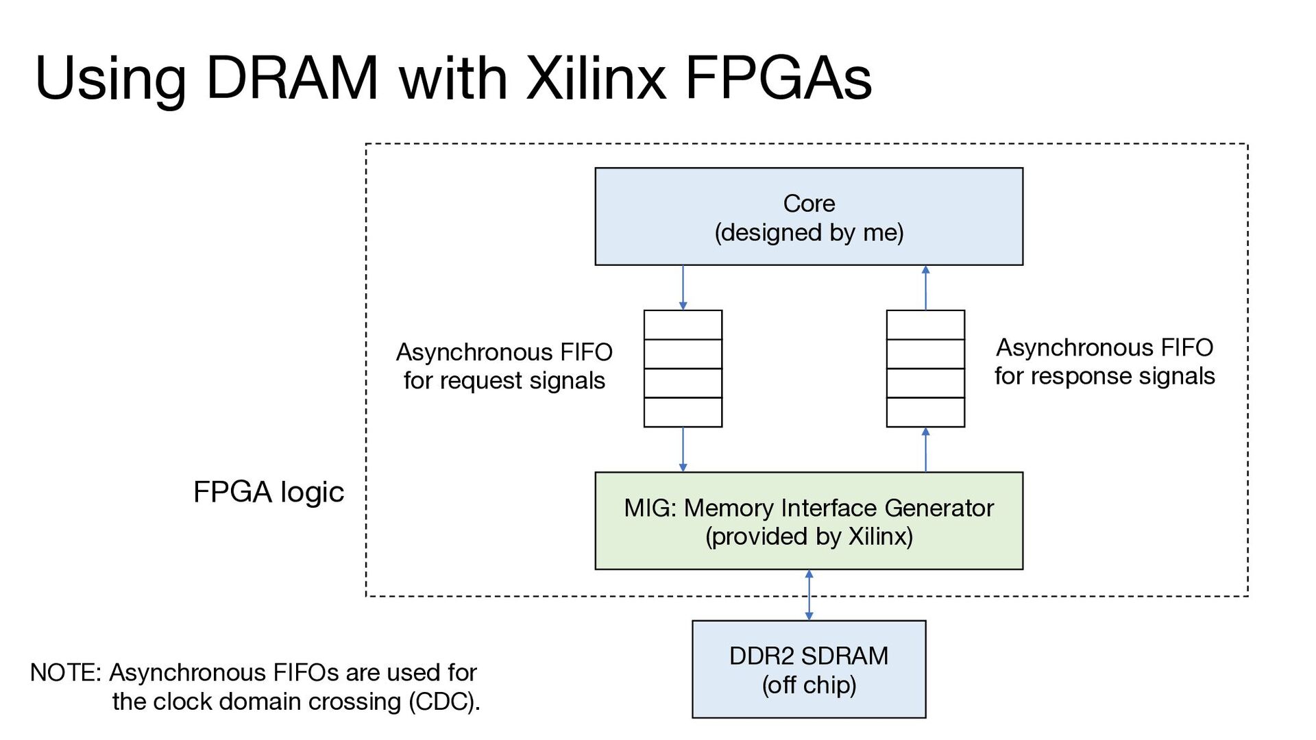
by Xilinx) DDR2 SDRAM (off chip) Core (designed by me) Asynchronous FIFO for response signals Asynchronous FIFO for request signals NOTE: Asynchronous FIFOs are used for the clock domain crossing (CDC). FPGA logic
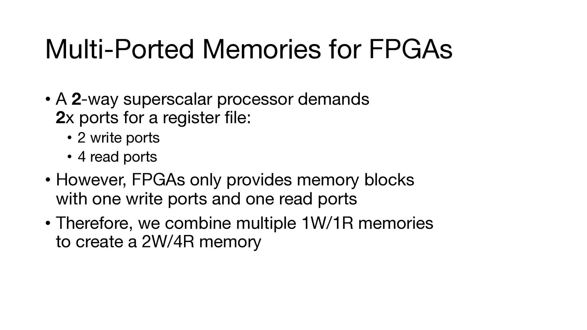
2x ports for a register file: • 2 write ports • 4 read ports • However, FPGAs only provides memory blocks with one write ports and one read ports • Therefore, we combine multiple 1W/1R memories to create a 2W/4R memory
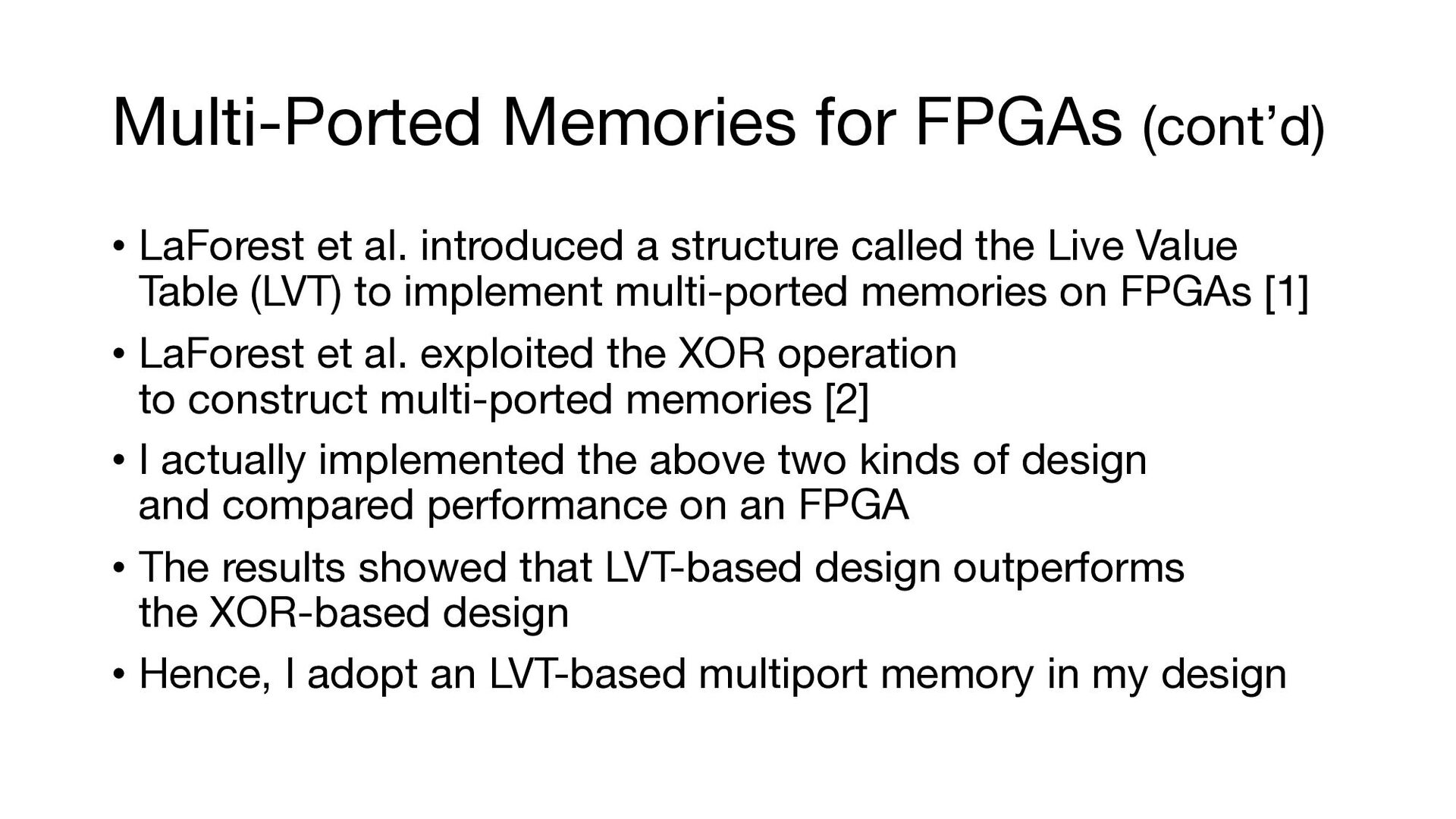
a structure called the Live Value Table (LVT) to implement multi-ported memories on FPGAs [1] • LaForest et al. exploited the XOR operation to construct multi-ported memories [2] • I actually implemented the above two kinds of design and compared performance on an FPGA • The results showed that LVT-based design outperforms the XOR-based design • Hence, I adopt an LVT-based multiport memory in my design
Efficient multi-ported memories for FPGAs. In Proceedings of the 18th annual ACM/SIGDA international symposium on Field programmable gate arrays (FPGA '10). Association for Computing Machinery, New York, NY, USA, 41–50. [2] Charles Eric Laforest, Ming G. Liu, Emma Rae Rapati, and J. Gregory Steffan. 2012. Multi-ported memories for FPGAs via XOR. In Proceedings of the ACM/SIGDA international symposium on Field Programmable Gate Arrays (FPGA '12). Association for Computing Machinery, New York, NY, USA, 209–218.
![References [1] Charles Eric LaForest and J. Gregory Steffan. 2010.](https://files.speakerdeck.com/presentations/e770640dd3ea42cd88d0cf4085ced335/slide_19.jpg)