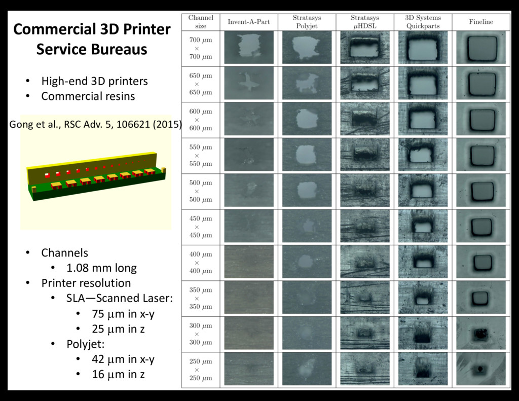
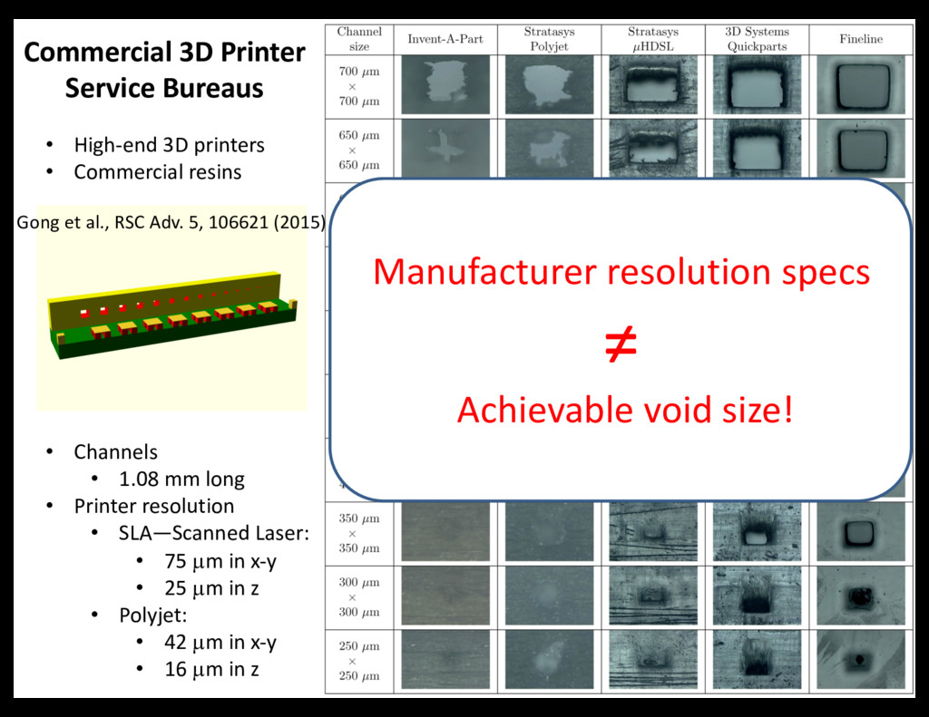
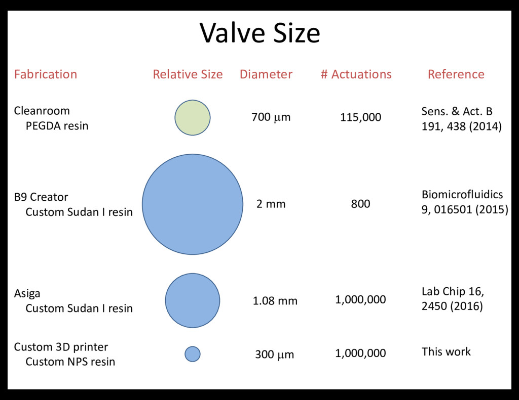
Commercial resins • Channels • 1.08 mm long • Printer resolution • SLA—Scanned Laser: • 75 µm in x-y • 25 µm in z • Polyjet: • 42 µm in x-y • 16 µm in z Gong et al., RSC Adv. 5, 106621 (2015)
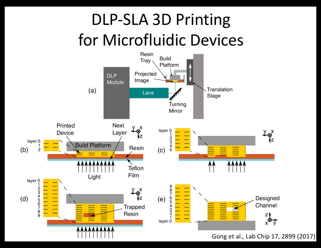
Mirror Resin Tray Build Platform Translation Stage Projected Image Light layer 0 1 2 Build Platform Resin Printed Device Next Layer Teflon Film y z x 9 8 7 6 5 4 3 2 1 layer 0 Designed Channel y z x layer 0 1 2 3 4 5 y z x Trapped Resin layer 0 1 2 3 4 5 6 7 8 9 y z x (a) (b) (d) (c) (e) Gong et al., Lab Chip 17, 2899 (2017)
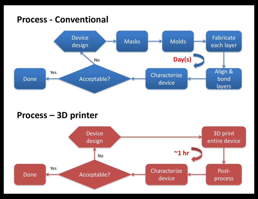
Align & bond layers Characterize device Acceptable? Done Yes No ~1 hr Process – 3D printer Device design 3D print entire device Post- process Characterize device Acceptable? Done Yes No Day(s)
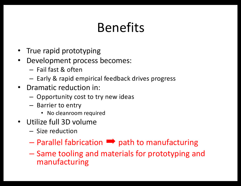
Fail fast & often – Early & rapid empirical feedback drives progress • Dramatic reduction in: – Opportunity cost to try new ideas – Barrier to entry • No cleanroom required • Utilize full 3D volume – Size reduction – Parallel fabrication ➡ path to manufacturing – Same tooling and materials for prototyping and manufacturing
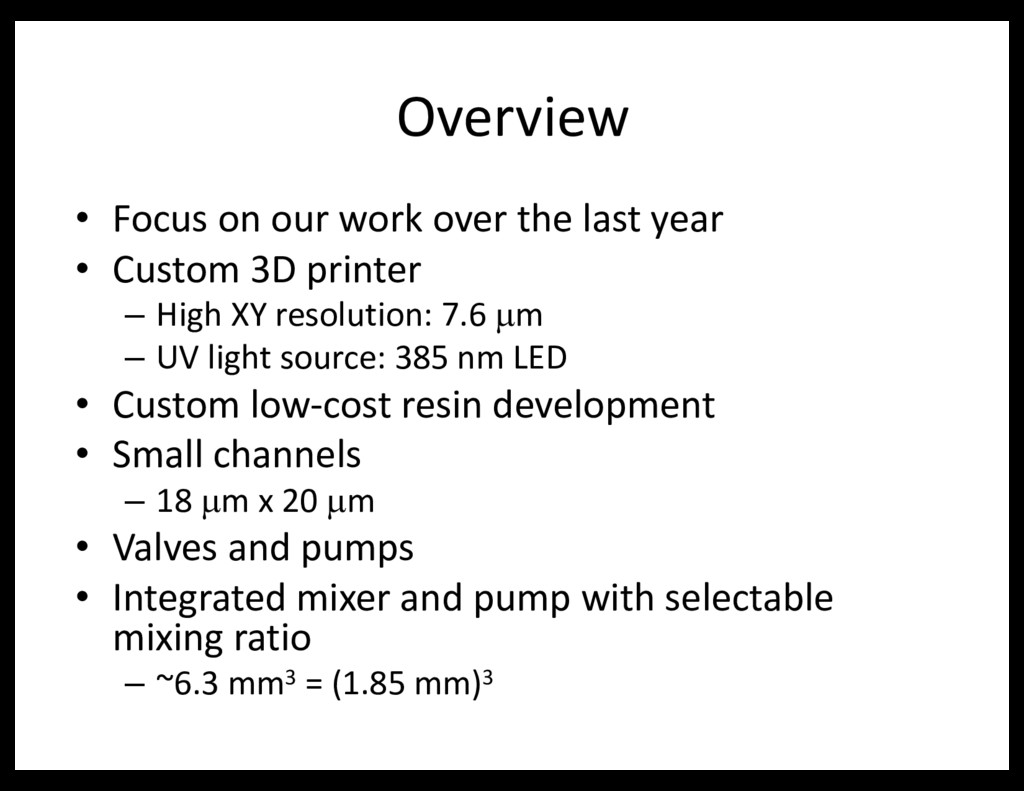
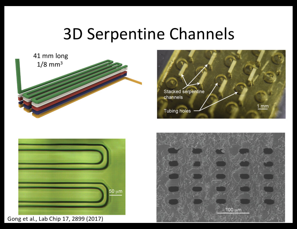
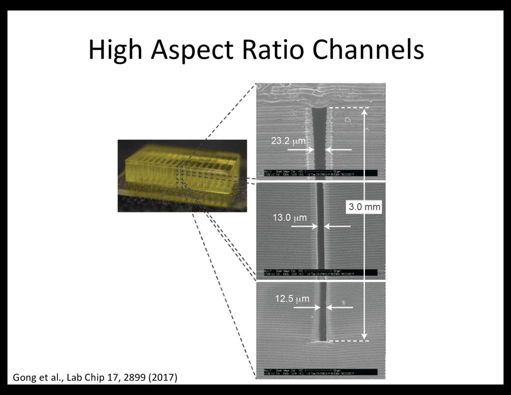
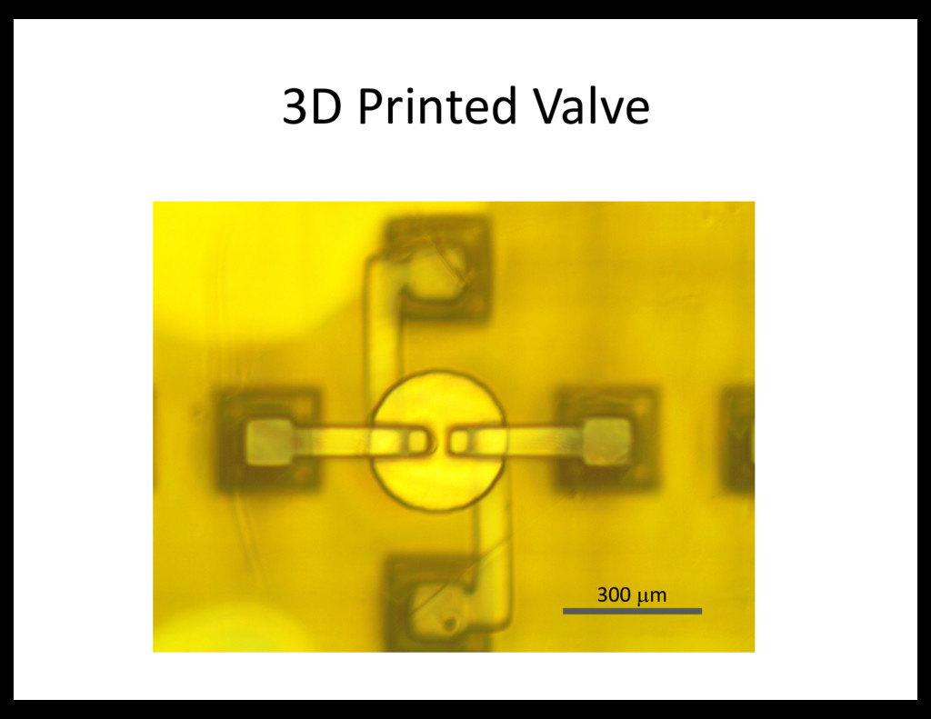
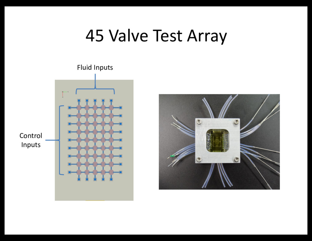
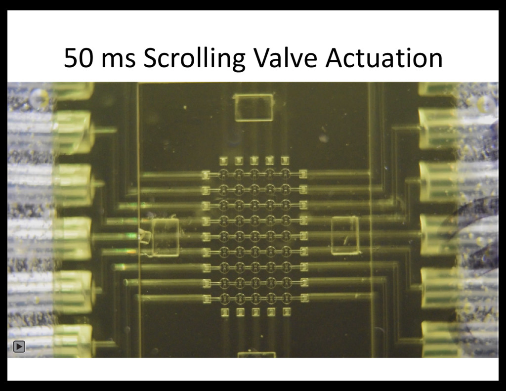
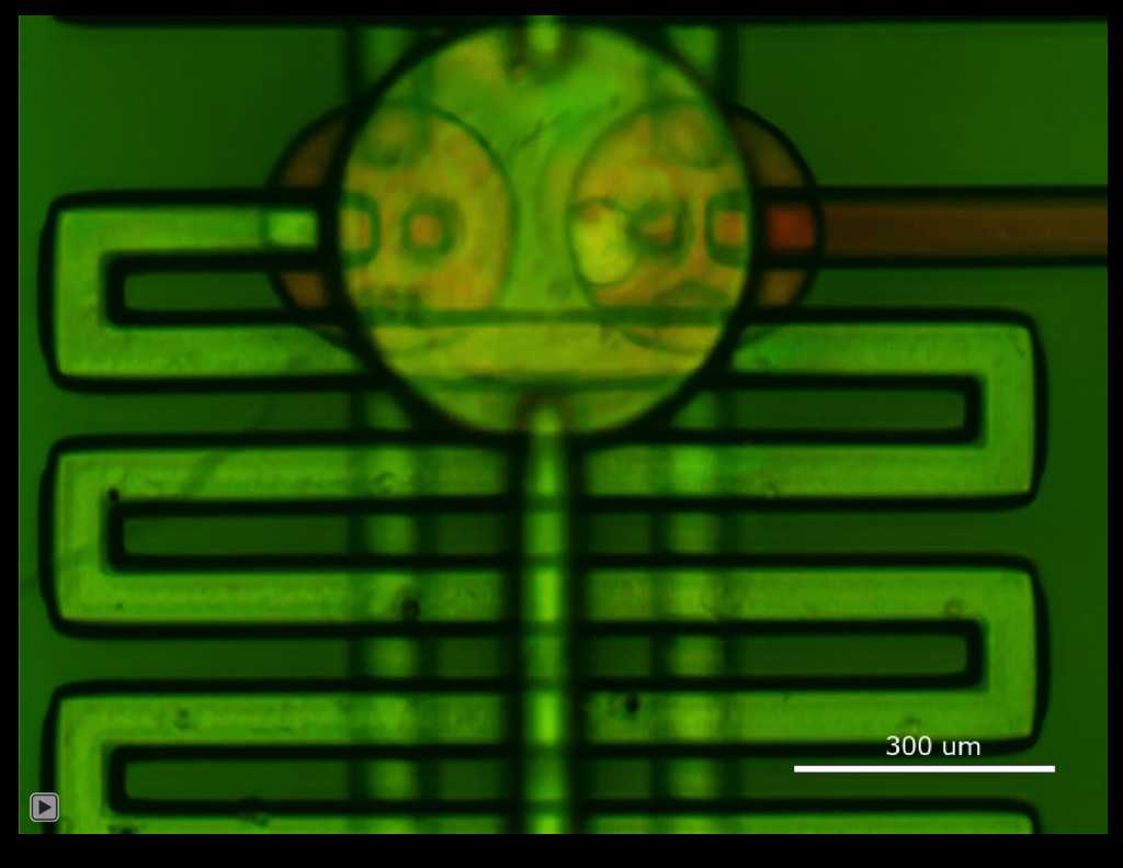
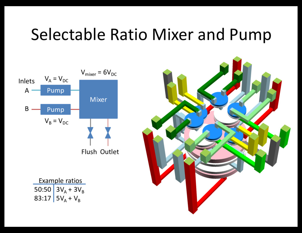
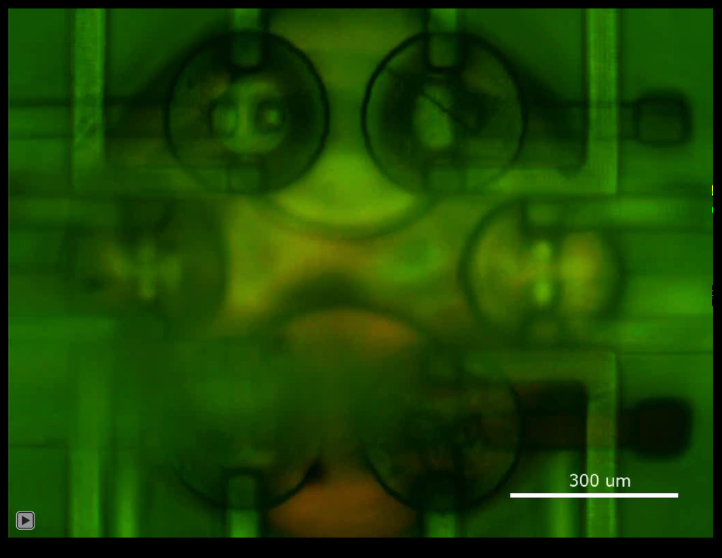
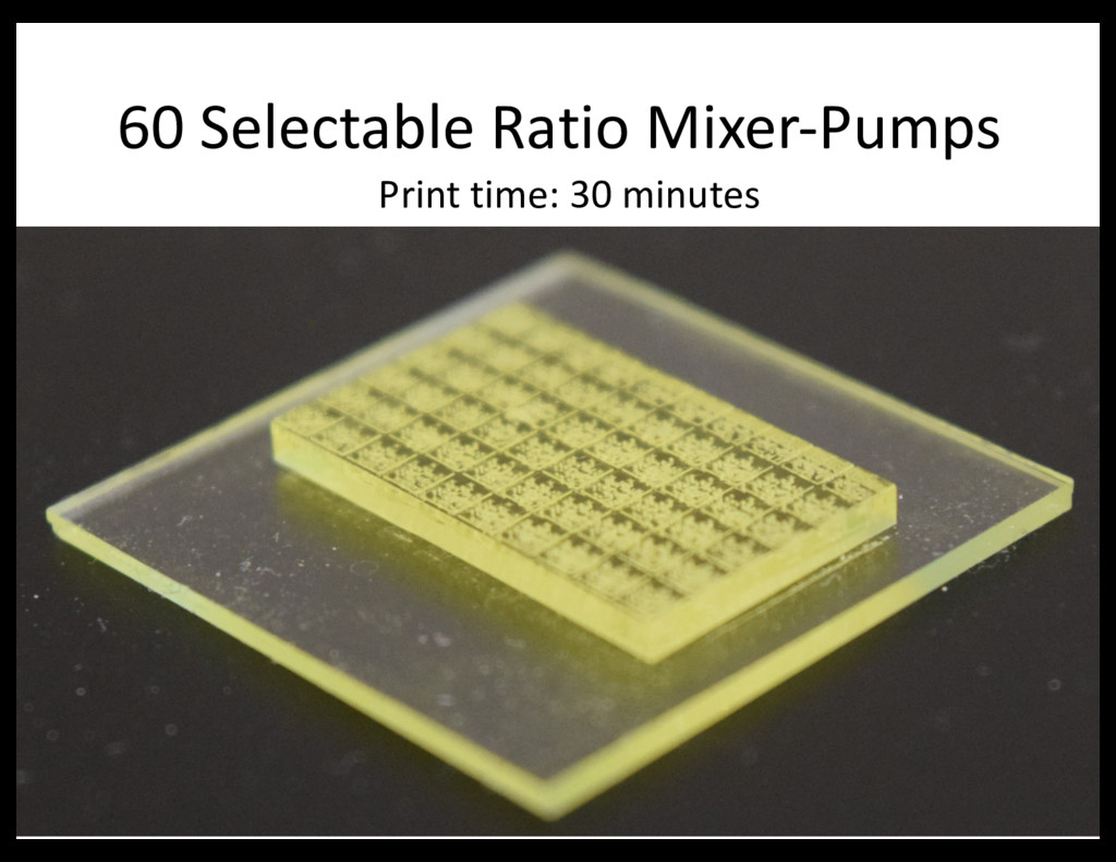
• Custom 3D printer – High XY resolution: 7.6 µm – UV light source: 385 nm LED • Custom low-cost resin development • Small channels – 18 µm x 20 µm • Valves and pumps • Integrated mixer and pump with selectable mixing ratio – ~6.3 mm3 = (1.85 mm)3
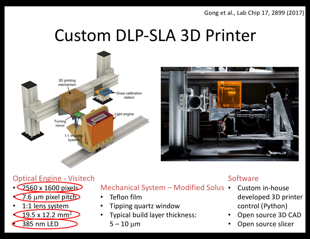
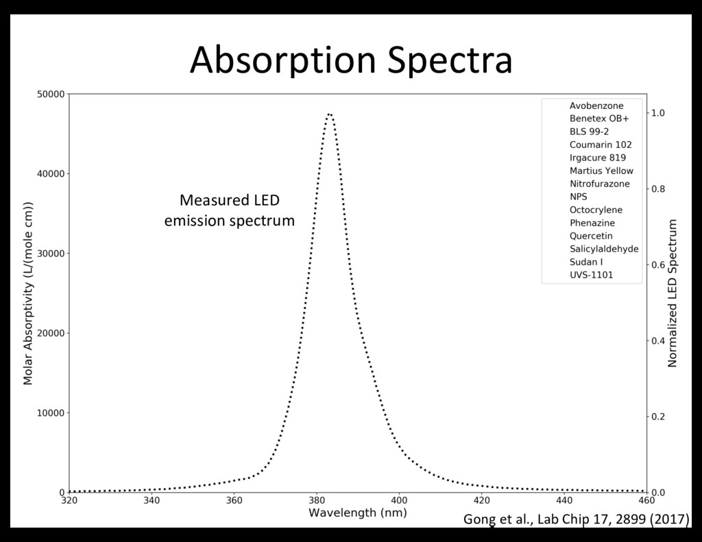
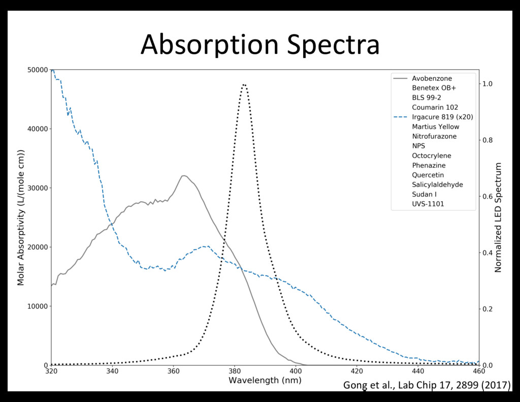
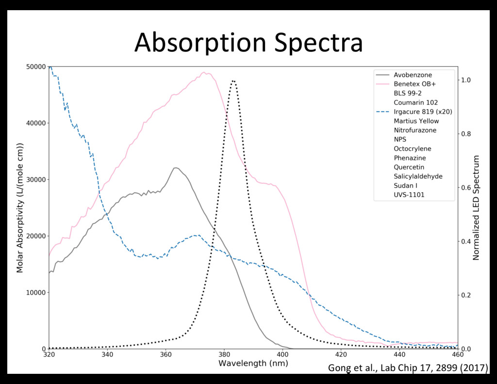
x 1600 pixels • 7.6 µm pixel pitch • 1:1 lens system • 19.5 x 12.2 mm2 • 385 nm LED Mechanical System – Modified Solus • Teflon film • Tipping quartz window • Typical build layer thickness: 5 – 10 µm Software • Custom in-house developed 3D printer control (Python) • Open source 3D CAD • Open source slicer Gong et al., Lab Chip 17, 2899 (2017)
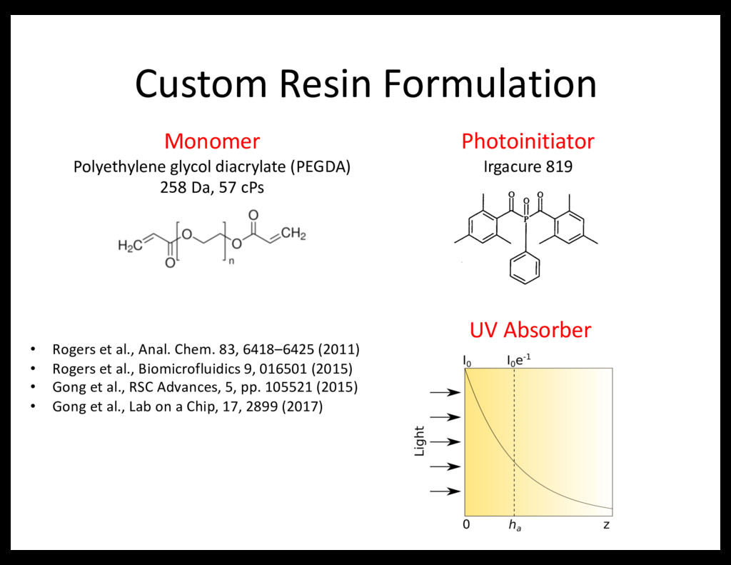
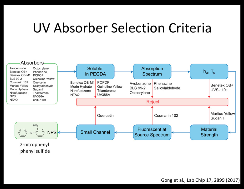
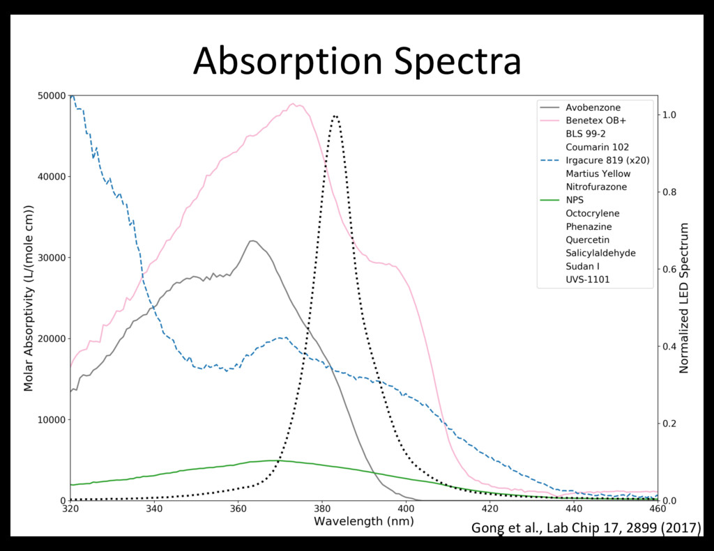
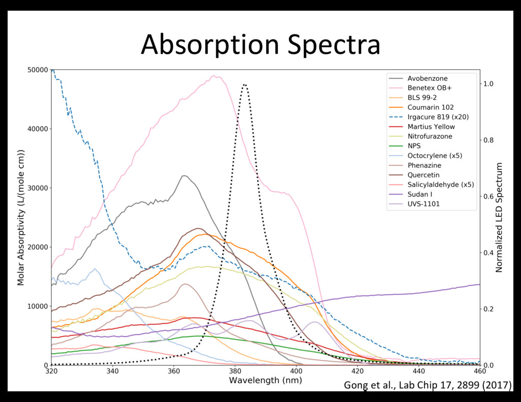
Rogers et al., Biomicrofluidics 9, 016501 (2015) • Gong et al., RSC Advances, 5, pp. 105521 (2015) • Gong et al., Lab on a Chip, 17, 2899 (2017) Custom Resin Formulation Monomer Polyethylene glycol diacrylate (PEGDA) 258 Da, 57 cPs Photoinitiator Irgacure 819 UV Absorber
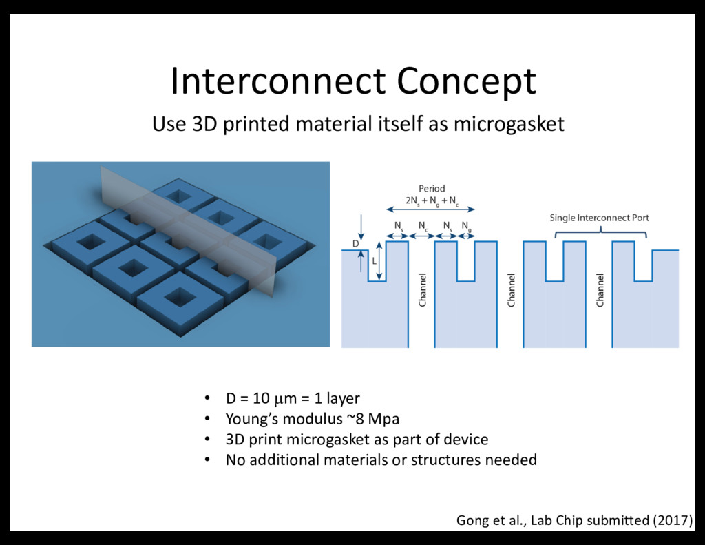
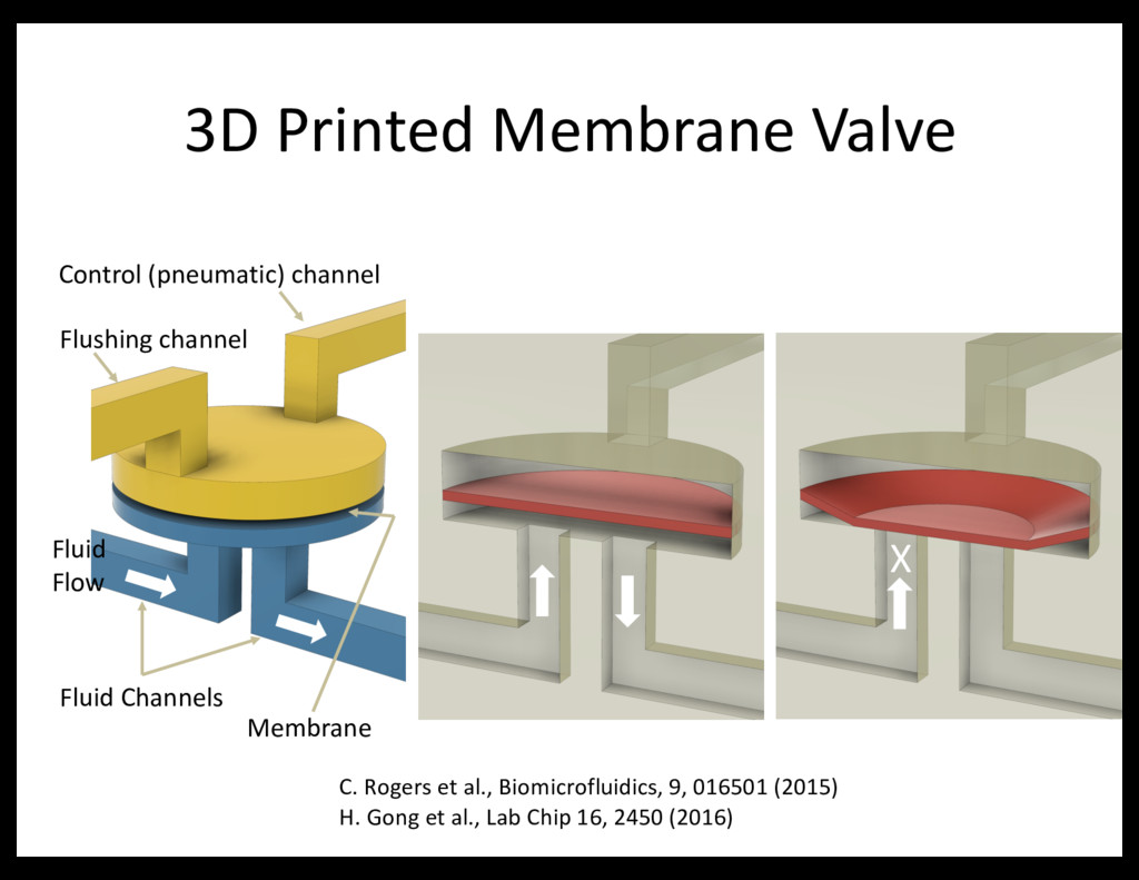
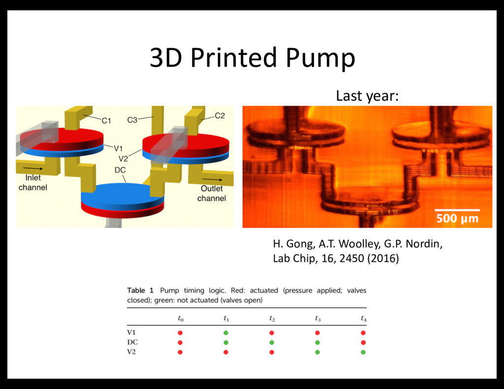
• Young’s modulus ~8 Mpa • 3D print microgasket as part of device • No additional materials or structures needed Use 3D printed material itself as microgasket Gong et al., Lab Chip submitted (2017)
– Complete control over operation of printer • Resins – Small ha – Must be tailored to emission spectrum – Open source • Explore 3D structures – Get away from conventional 2D thinking • Components • Layout – Experiment-based exploration of parameter space and performance optimization • Automated design – Library of standard components – Automated layout – Specify functional processes ➝ automated design generation
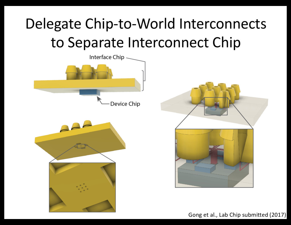
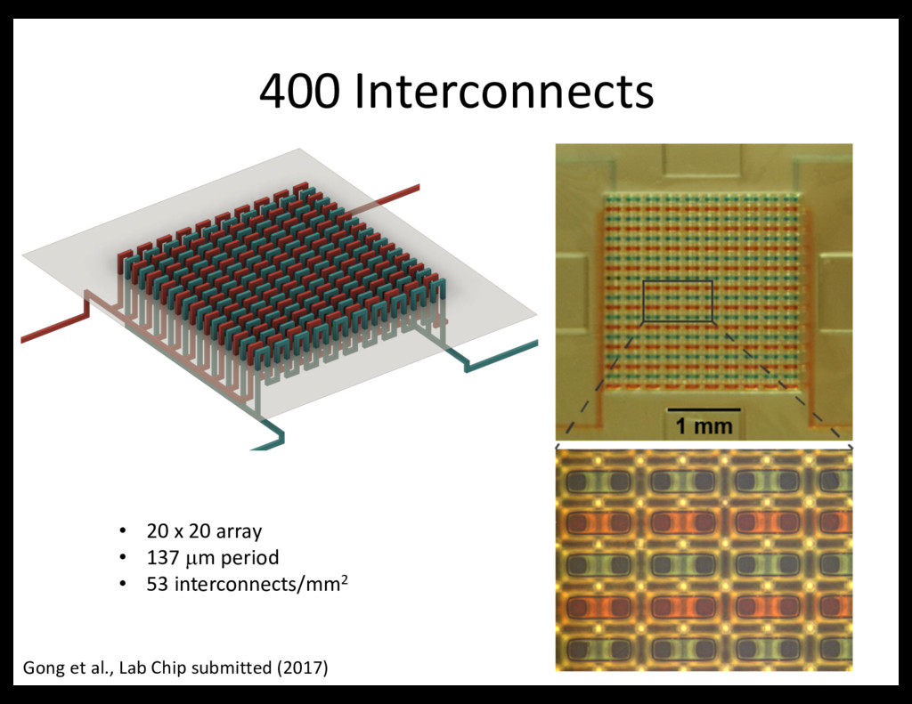
Microfluidic Interconnects • Mike Beauchamp, T184h Microchip Electrophoresis of Preterm Birth Biomarkers in 3D Printed Devices • Anna Nielson, M182h Separation of a Panel of Preterm Birth Biomarkers Using Microchip Electrophoresis