defects in pillars and nanowires •Mechanical behavior of free-standing copper thin films • stress-strain behavior of pre-strained thin films • Mechanisms that lead to the observed behavior •Comparing with other FCC metals • Comparison motivated by mechanistic understanding of copper thin films
removal of the ILD layers (www.ibm.com) Cross-sectional view of the dual damascene structure (www.ibm.com) Schematic of the strained SiGe p-channel heterostructure MOSFET Silicon Nanowire Transistor (NIST Illustration)
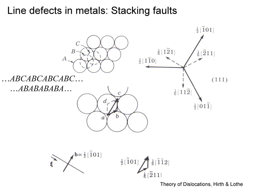
Fig. A.6. Given a layer A, can be extended by stacking the next layer so that its atoms occupy B or A, B, and C refer to the three possible layer positions in a projection norm packed layers. The stacking sequence corresponding to an fc …ABCABCABCABC…, while that for a hcp crystal is …ABABABABA partial dislocation is created in a fcc crystal, the fcc stacking sequence hcp stacking sequence; the stacking sequence in the crystal with a stackin …ABCABCACABCABC…. 6. Given a layer A, close packing atoms occupy B or C sites. Here a projection normal to the close- onding to an fcc crystal is is …ABABABABA…. When a tacking sequence changes to the ystal with a stacking fault can be Line defects in metals: Stacking faults Theory of Dislocations, Hirth & Lothe
a samples and a comparison t to the theoretical shear stren All data points represent the geneously during compressio 2͑b͒. It is clear from the grap which were never subjected flow stresses higher than bul rise in strength as the diamet Ga+ removal and pretest-ann on the curve formed by the F believe that observed size e fabrication technique. Whil image of a compressed pillar after deformation. Slip lines in multiple orientations are clearly present change. Mechanical behavior of bulk J. Greer et al. Phys. Rev. B. 73, 245410 (2006) R. Madec et al., Phys. Rev. Lett. 89, 255508 (2002) http://www.geol.ucsb.edu Au
were annealed at 300 °C to remo remaining defects. Figure 4 presents flow stresses aforementioned samples as well as the FIB-fab samples and a comparison to the axial stress corresp to the theoretical shear strength calculated by Ogata All data points represent the pillars which deformed geneously during compression testing, as can be seen 2͑b͒. It is clear from the graph that the electroplated which were never subjected to the Ga+ ions, not onl flow stresses higher than bulk gold but also exhibit a rise in strength as the diameter is reduced. It is also cle Ga+ removal and pretest-annealing resulted in data th on the curve formed by the FIB pillars. This result lead believe that observed size effect is not linked to a s fabrication technique. While some minimal Ga+ mi image of a compressed pillar after deformation. Slip lines in multiple orientations are clearly present and indicate a homogeneou change. Au single crystal pillars were annealed at 300 °C to r remaining defects. Figure 4 presents flow stre aforementioned samples as well as the FIB samples and a comparison to the axial stress cor to the theoretical shear strength calculated by Og All data points represent the pillars which defor geneously during compression testing, as can be s 2͑b͒. It is clear from the graph that the electropla which were never subjected to the Ga+ ions, no flow stresses higher than bulk gold but also exhib rise in strength as the diameter is reduced. It is als Ga+ removal and pretest-annealing resulted in da on the curve formed by the FIB pillars. This result believe that observed size effect is not linked to fabrication technique. While some minimal Ga formation. Stress-strain curves of FIB pillars whose diam- eters range between 290 nm and 7450 nm as well as the strength of bulk gold at 2% strain are presented in Fig. 2͑a͒. Uniaxial loading in the ͗001͘ direction, chosen for our ex- periments and corresponding to a high-symmetry orientation, ¯ FIG. 1. ͑a͒ A representative ͗001͘-oriented gold pillar machined in the FIB. Pillar diameter=290 nm, pillar height=1.2 m. ͑b͒ A large pillar ͑7.45 m diameter͒ and a small pillar ͑250 nm diameter͒. J. Greer et al. Phys. Rev. B. 73, 245410 (2006) Au
20 30 40 50 50 Displacement (nm) Force (µN) 150 100 200 0 50 100 150 200 0 10 20 30 40 50 60 70 80 Displacement (nm) Force (µN) 250 300 350 400 0 0 0.2 0.4 0.6 0.8 1.0 1.2 1.4 50 100 150 200 Displacement (nm) Stress (GPa) 250 300 350 400 Test 1 Test 2 a d b e c f 200 nm g = [111] ZA = [110] [111] 200 nm 200 nm ure 1 Two consecutive in situ TEM compression tests on a FIB microfabricated 160-nm-top-diameter Ni pillar with 111⇥ orientation. a, Dark-field TEM image pillar before the tests; note the high initial dislocation density. b, Dark-field TEM image of the same pillar after the first test; the pillar is now free of dislocations. Z. Shan et al., Nature Materials 7, 115 (2007)
defects in pillars and nanowires •Mechanical behavior of free-standing copper thin films • stress-strain behavior of pre-strained thin films • Mechanisms that lead to the observed behavior •Comparing with other FCC metals • Comparison motivated by mechanistic understanding of copper thin films
dynamic deformation molecular-dynamics (MD) simulations 13 ection of interacting atoms following classical mechanics. For a system g N atoms with positions {r i } i=1 N and velocities {! i = dr i / dt} i=1 N , the tot ian is given by H({r i } i=1 N ) = T+ U = 1 2 m i ! i 2 + U({r i } i=1 N ) i=1 n " (2.1) • Embedded-Atom-Method (EAM) potential • Supercell size: up to 1.54 million atoms • Film thickness varied from 4 nm to 10 nm • Applied equi-biaxial tensile strain through cell size expansion: – applied strain rate: 107 s-1 - 1011 s-1
Strain rate 4 orders of magnitute lower than that during prestraining Stage I : Near elastic response and depletion of 15% of dislocations Stage II : Easy-glide; dislocation annihilation Stage III : Insufficient plastic flow; stress increases Stage III+: Nucleation of additional dislocations; material failure
Stage I : Near elastic response and depletion of 15% of dislocations Stage II : Easy-glide; dislocation annihilation Stage III : Insufficient plastic flow; stress increases Stage III+: Nucleation of additional dislocations; material failure
defects in pillars and nanowires •Mechanical behavior of free-standing copper thin films • stress-strain behavior of pre-strained thin films • Mechanisms that lead to the observed behavior •Comparing with other FCC metals • Comparison motivated by mechanistic understanding of copper thin films
defects in pillars and nanowires •Mechanical behavior of free-standing copper thin films • stress-strain behavior of pre-strained thin films • Mechanisms that lead to the observed behavior •Comparing with other FCC metals • Comparison motivated by mechanistic understanding of copper thin films
In stage II: Ni and Cu Constant stress and dislocations annihilate Al Stress increases monotonically Al Dislocations annihilate at half the rate 35% more annihilation in Ni and Cu than in Al
In stage II: In Ni and Cu, plastic strain decreases monotonically In Al, plastic strain remains constant Critical plastic strain beyond which stress increases in every thinfilm In Al, plastic strain never exceeds critical plastic strain