misfit dislocations Kedarnath Kolluri and Blas Uberuaga MST-8, Los Alamos National Lab, NM 87545 Acknowledgments: Louis Vernon, Satyesh Yadav, Michael Demkowicz, John Hirth, Richard Hoagland, Amit Misra, and Gopinath Subramanian
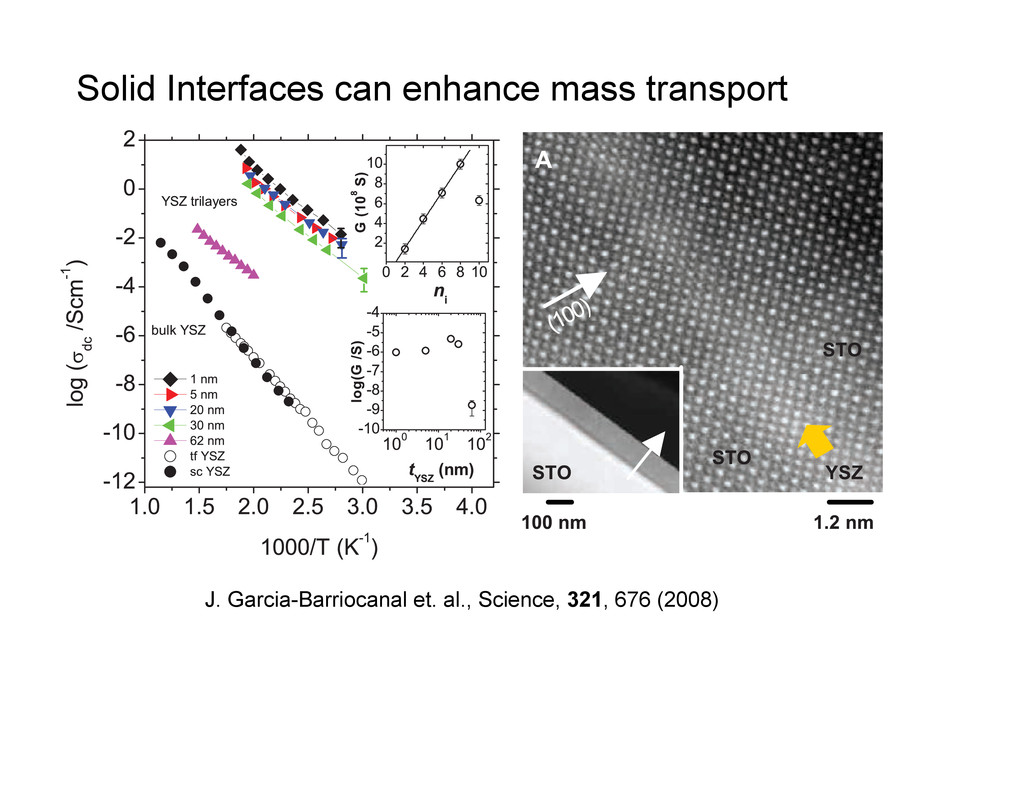
material, which imposes rather high operational temperatures around 800°C (1–4). The search for alternative electrolytes has not yet been successful in reaching the conduc- tivity value of 0.01 S/cm desired for room tem- perature operation (1–4). Only modest reductions in the operation temperature of SOFCs (500° to 700°C) can be anticipated with the recently proposed optimized electrolytes such as gadolinia-doped ceria and lanthanum gallates (8–11). On the other hand, the one to two orders of magnitude increase of the electrical conductivity reported (12–14) in nano- crystalline samples as compared with single crys- tals outlines the importance of processing as an alternative route to increasing conductivity values toward the desired levels. Because modern thin film growth techniques allow a precise control of layer thickness and morphology, they provide a pathway for the production of solid electrolytes with optimized properties. Maier et al. found a substantial increase of the dc ionic conductivity of superlattices of CaF2 and BaF2 when the thickness of the individual layers was decreased down to 16 nm, assigned to a size effect due to the space charge regions being smaller than the layer thickness (15, 16). Kosacki et al. have reported enhanced conductivity in highly tex- tured thin films of YSZ with thicknesses between 60 and 15 nm, reaching 0.6 S/cm at 800°C (17). Because reducing film thickness (and therefore increasing the fraction of material near the in- results (fig. S1), meaning that the ultrathin layer of YSZ grows rotated by 45° around the c axis and strains to match the STO lattice. Because the bulk lattice constants of STO and YSZ are range or sd obtained fr frequency p due to grai Fig. 1. (A) Z-contrast scanning transmission electron microscopy (S the [YSZ1nm /STO10nm ]9 superlattice (with nine repeats), obtain microscope. A yellow arrow marks the position of the YSZ layer. (In in the VG Microscopes HB501UX column. In both cases a white arrow spectra showing the O K edge obtained from the STO unit cell at the into the STO layer (black squares). (Inset) Ti L2,3 edges for the same are the result of averaging four individual spectra at these position Fig. 2. Real part of the lateral electrical conductivity versus fre- scaling, ductance the large res orig- abrupt conductivity decrease when the thickness changes from 30 to 62 nm is most likely due to a degraded interface structure when the YSZ layers exceed the critical thickness. the yers The nm. ystal hick minal ance as a ni . duct- rs at are con- on September 17, 2011 www.sciencemag.org J. Garcia-Barriocanal et. al., Science, 321, 676 (2008)
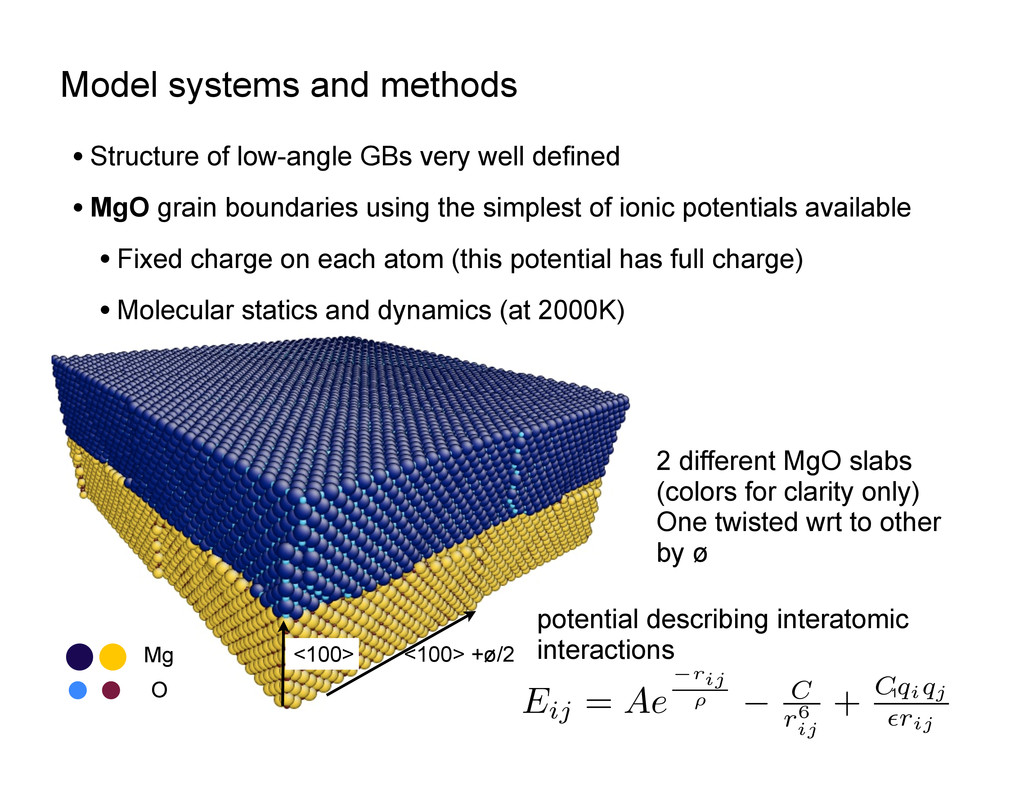
GBs very well defined • MgO grain boundaries using the simplest of ionic potentials available • Fixed charge on each atom (this potential has full charge) • Molecular statics and dynamics (at 2000K) <100> <100> +ø/2 Eij = Ae rij ⇢ C r6 ij + Cqiqj ✏rij 1 2 different MgO slabs (colors for clarity only) One twisted wrt to other by ø potential describing interatomic interactions Mg O
structures of GBs 3. Structure and energetics of a vacancy at (and near) GBs • compact and delocalized vacancies 4. Migrations of vacancies • observations and postulated mechanisms
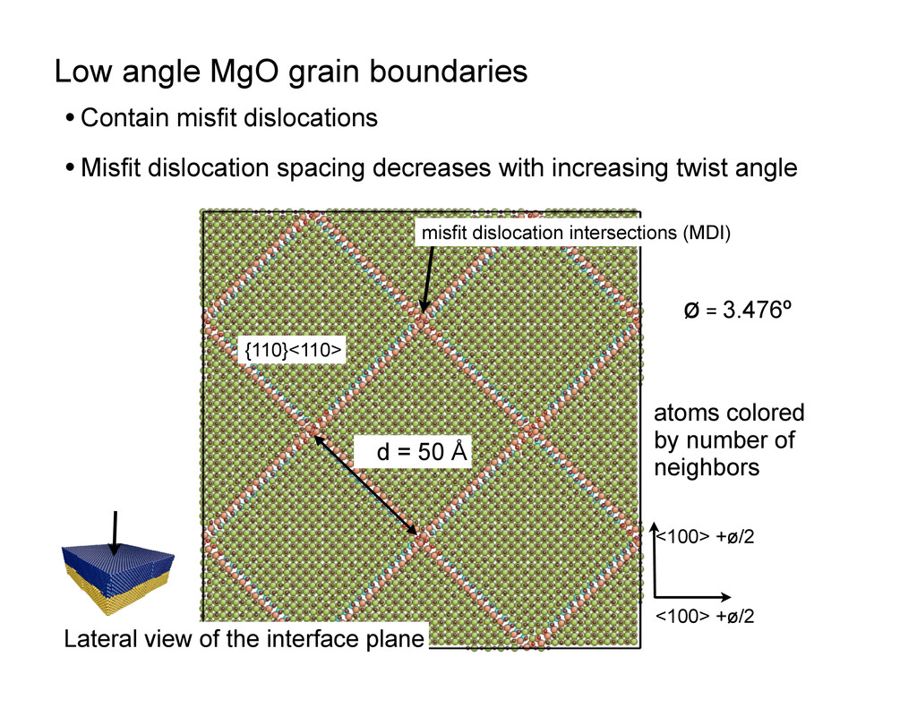
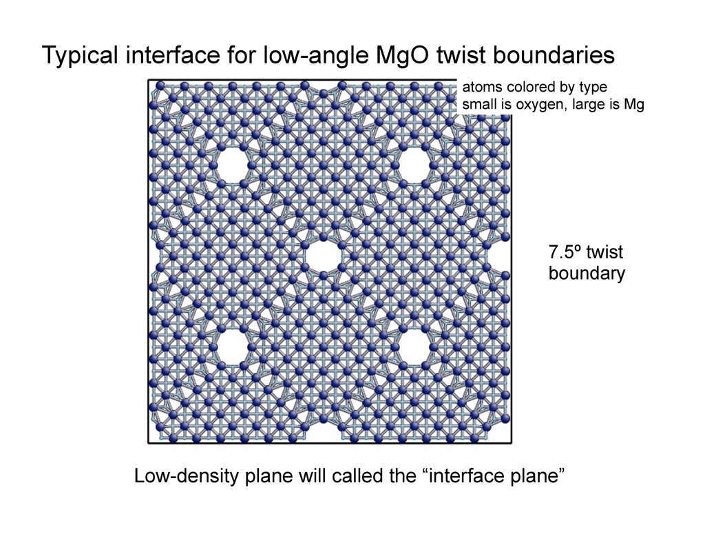
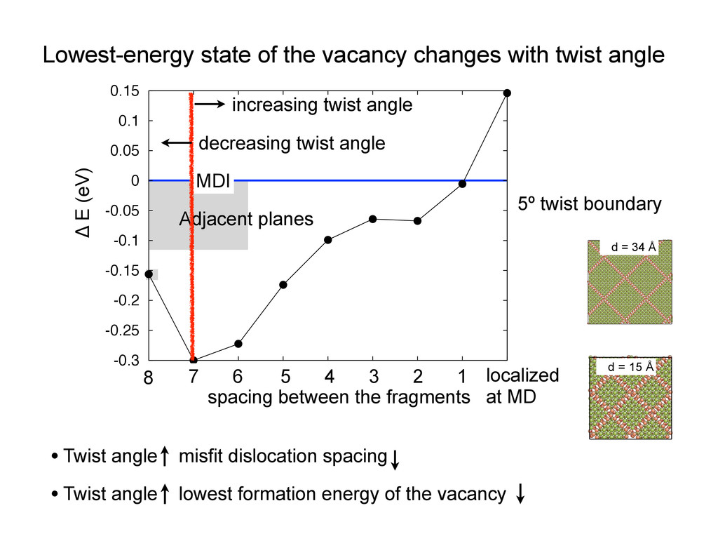
dislocations • Misfit dislocation spacing decreases with increasing twist angle d = 50 Å {110}<110> <100> +ø/2 <100> +ø/2 ø = 3.476º misfit dislocation intersections (MDI) atoms colored by number of neighbors Lateral view of the interface plane
methods 2. Ground-state structures of GBs 3. Structure and energetics of a vacancy at (and near) GBs • compact and delocalized vacancies 4. Transport of vacancies • observations and postulated mechanisms
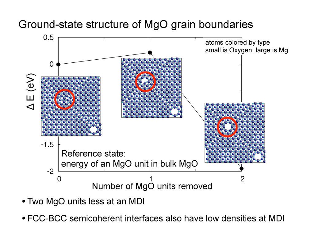
also have low densities at MDI -2 -1.5 -1 -0.5 0 0.5 0 0.5 1 1.5 2 Ground-state structure of MgO grain boundaries Reference state: energy of an MgO unit in bulk MgO Δ E (eV) atoms colored by type small is Oxygen, large is Mg Number of MgO units removed
methods 2. Ground-state structures of GBs 3. Structure and energetics of a vacancy at GBs • compact and delocalized vacancies 4. Transport of vacancies • observations and postulated mechanisms
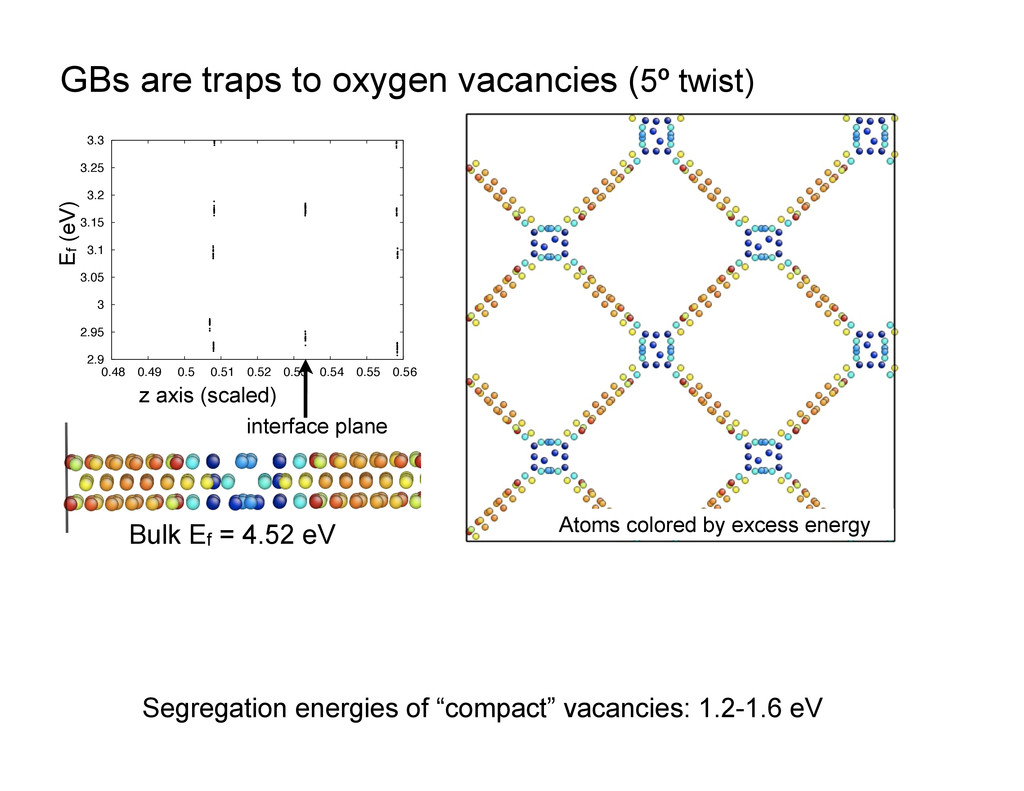
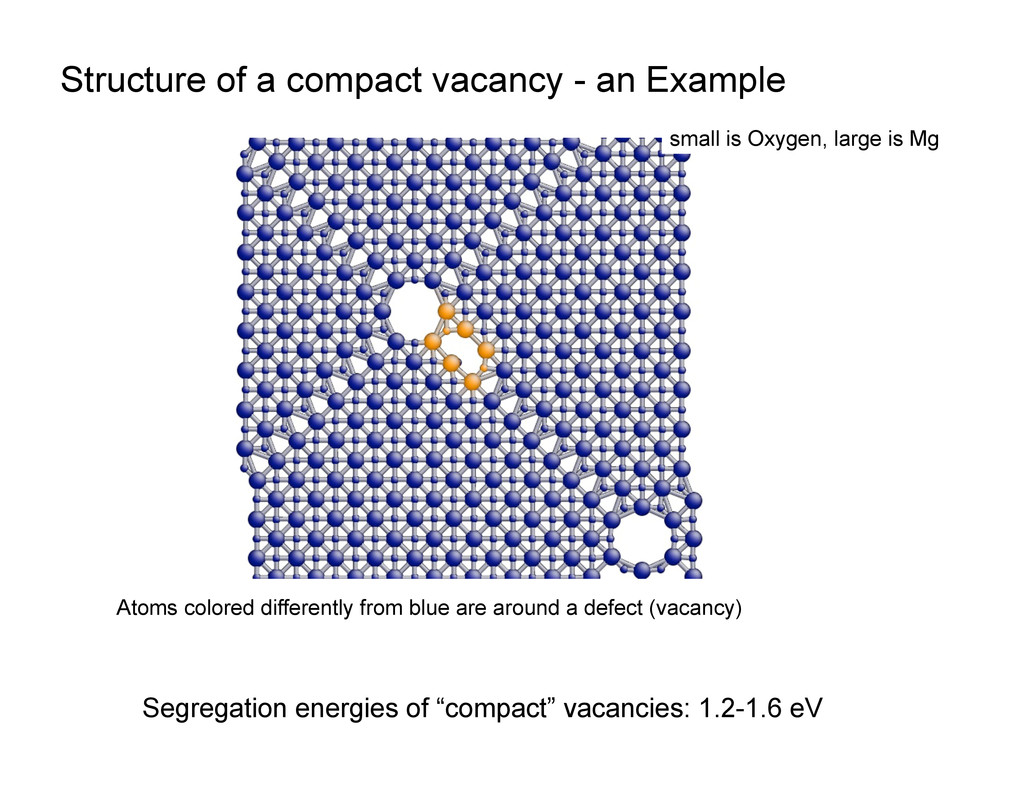
3 3.05 3.1 3.15 3.2 3.25 3.3 0.48 0.49 0.5 0.51 0.52 0.53 0.54 0.55 0.56 Segregation energies of “compact” vacancies: 1.2-1.6 eV Ef (eV) z axis (scaled) interface plane Bulk Ef = 4.52 eV Atoms colored by excess energy
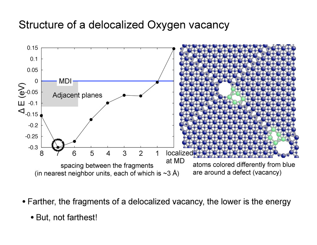
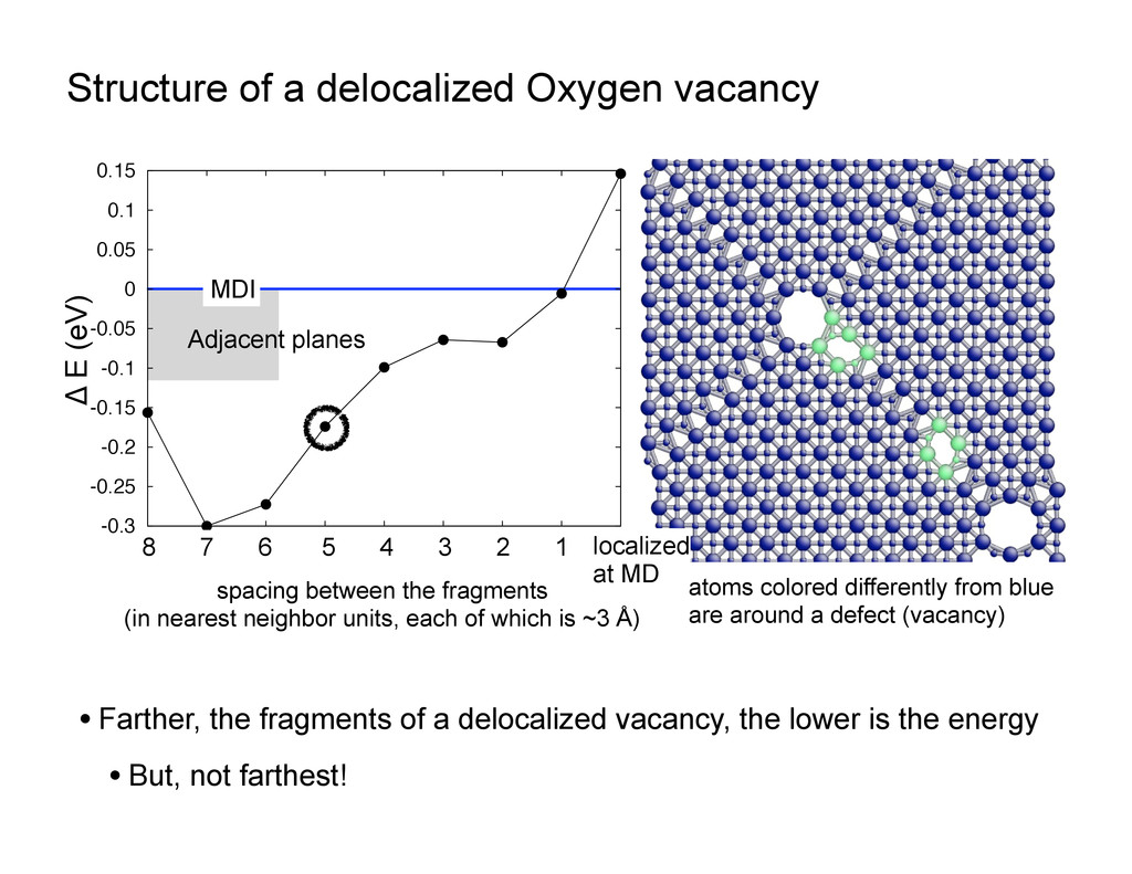
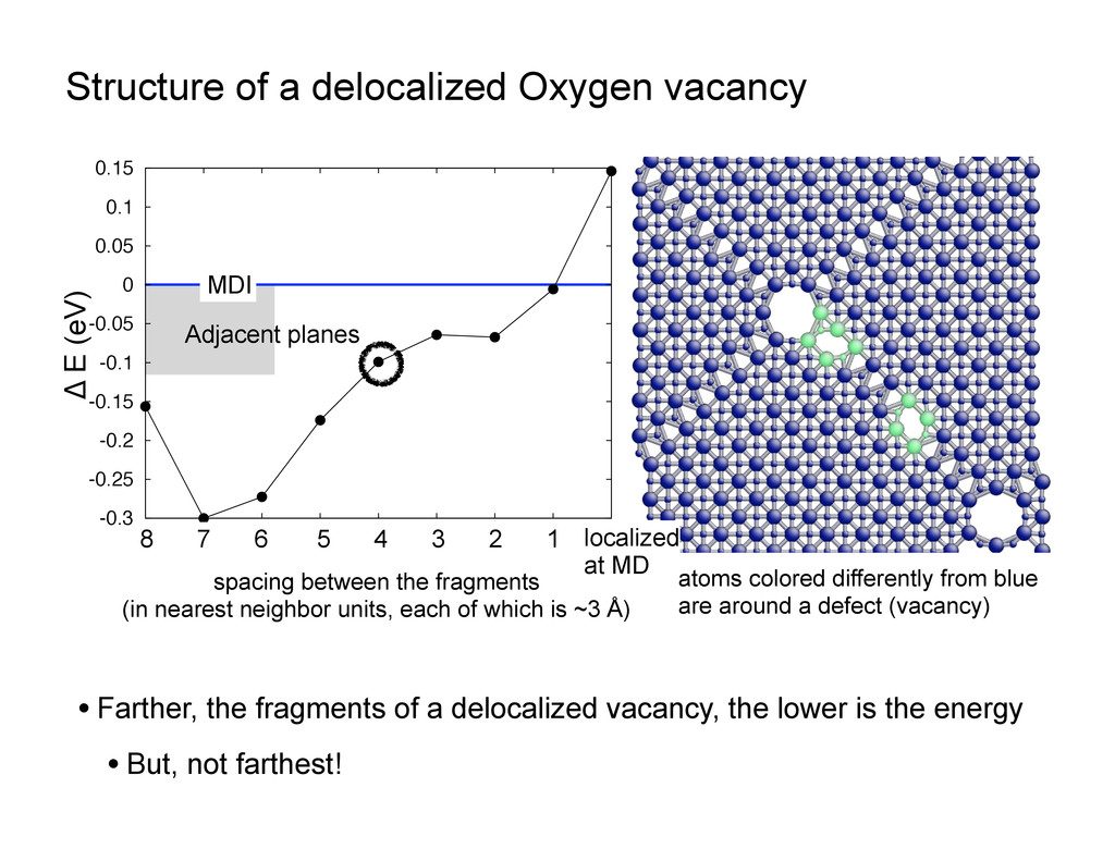
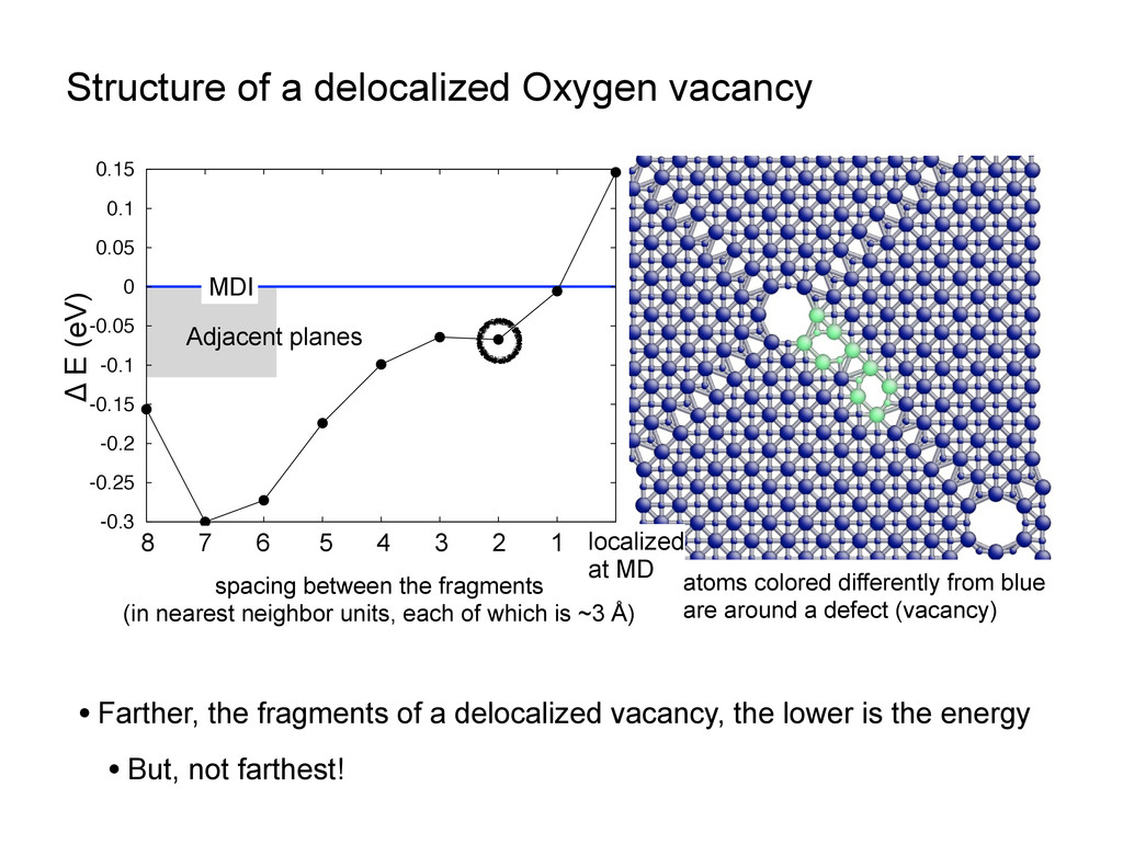
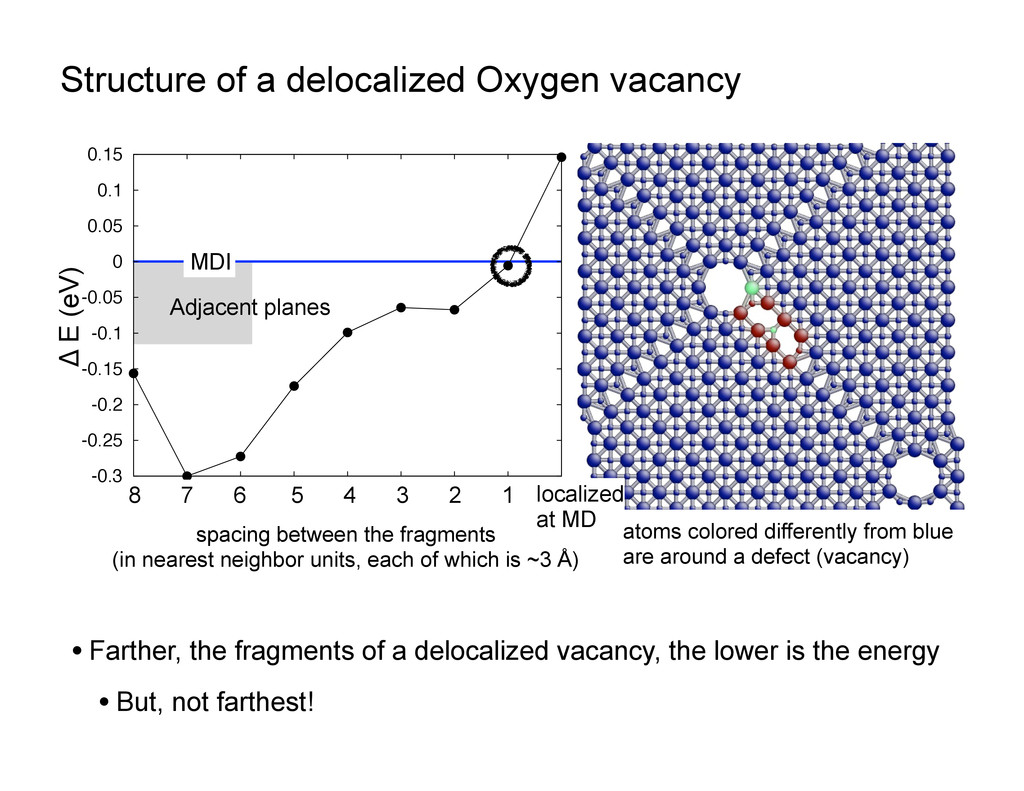
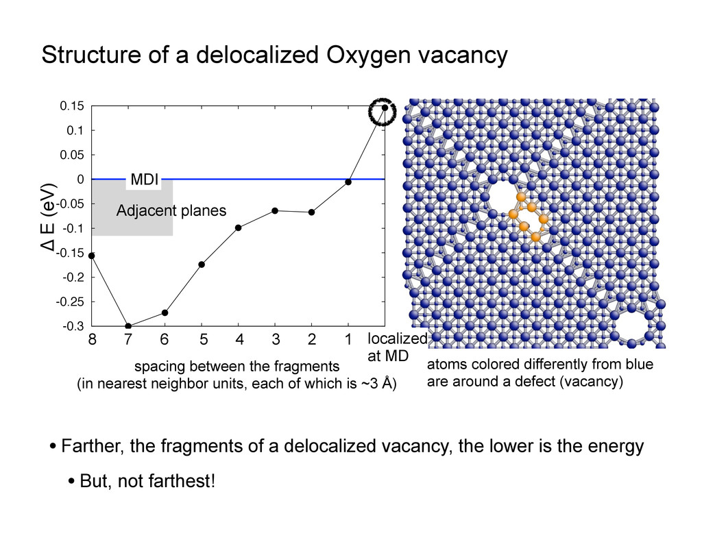
of a delocalized vacancy, the lower is the energy • But, not farthest! atoms colored differently from blue are around a defect (vacancy) Δ E (eV) spacing between the fragments (in nearest neighbor units, each of which is ~3 Å) MDI Adjacent planes -0.3 -0.25 -0.2 -0.15 -0.1 -0.05 0 0.05 0.1 0.15 0 1 2 3 4 5 6 7 8 1 2 3 4 5 6 7 localized at MD 8
is the energy • But, not farthest! atoms colored differently from blue are around a defect (vacancy) Structure of a delocalized Oxygen vacancy Δ E (eV) spacing between the fragments (in nearest neighbor units, each of which is ~3 Å) MDI Adjacent planes -0.3 -0.25 -0.2 -0.15 -0.1 -0.05 0 0.05 0.1 0.15 0 1 2 3 4 5 6 7 8 1 2 3 4 5 6 7 localized at MD 8
is the energy • But, not farthest! atoms colored differently from blue are around a defect (vacancy) Structure of a delocalized Oxygen vacancy Δ E (eV) spacing between the fragments (in nearest neighbor units, each of which is ~3 Å) MDI Adjacent planes -0.3 -0.25 -0.2 -0.15 -0.1 -0.05 0 0.05 0.1 0.15 0 1 2 3 4 5 6 7 8 1 2 3 4 5 6 7 localized at MD 8
is the energy • But, not farthest! atoms colored differently from blue are around a defect (vacancy) Structure of a delocalized Oxygen vacancy Δ E (eV) spacing between the fragments (in nearest neighbor units, each of which is ~3 Å) MDI Adjacent planes -0.3 -0.25 -0.2 -0.15 -0.1 -0.05 0 0.05 0.1 0.15 0 1 2 3 4 5 6 7 8 1 2 3 4 5 6 7 localized at MD 8
is the energy • But, not farthest! atoms colored differently from blue are around a defect (vacancy) Structure of a delocalized Oxygen vacancy Δ E (eV) spacing between the fragments (in nearest neighbor units, each of which is ~3 Å) MDI Adjacent planes -0.3 -0.25 -0.2 -0.15 -0.1 -0.05 0 0.05 0.1 0.15 0 1 2 3 4 5 6 7 8 1 2 3 4 5 6 7 localized at MD 8
is the energy • But, not farthest! atoms colored differently from blue are around a defect (vacancy) Structure of a delocalized Oxygen vacancy Δ E (eV) spacing between the fragments (in nearest neighbor units, each of which is ~3 Å) MDI Adjacent planes -0.3 -0.25 -0.2 -0.15 -0.1 -0.05 0 0.05 0.1 0.15 0 1 2 3 4 5 6 7 8 1 2 3 4 5 6 7 localized at MD 8
is the energy • But, not farthest! atoms colored differently from blue are around a defect (vacancy) Structure of a delocalized Oxygen vacancy Δ E (eV) spacing between the fragments (in nearest neighbor units, each of which is ~3 Å) MDI Adjacent planes -0.3 -0.25 -0.2 -0.15 -0.1 -0.05 0 0.05 0.1 0.15 0 1 2 3 4 5 6 7 8 1 2 3 4 5 6 7 localized at MD 8
is the energy • But, not farthest! atoms colored differently from blue are around a defect (vacancy) Structure of a delocalized Oxygen vacancy Δ E (eV) spacing between the fragments (in nearest neighbor units, each of which is ~3 Å) MDI Adjacent planes -0.3 -0.25 -0.2 -0.15 -0.1 -0.05 0 0.05 0.1 0.15 0 1 2 3 4 5 6 7 8 1 2 3 4 5 6 7 localized at MD 8
is the energy • But, not farthest! atoms colored differently from blue are around a defect (vacancy) Structure of a delocalized Oxygen vacancy Δ E (eV) spacing between the fragments (in nearest neighbor units, each of which is ~3 Å) MDI Adjacent planes -0.3 -0.25 -0.2 -0.15 -0.1 -0.05 0 0.05 0.1 0.15 0 1 2 3 4 5 6 7 8 1 2 3 4 5 6 7 localized at MD 8
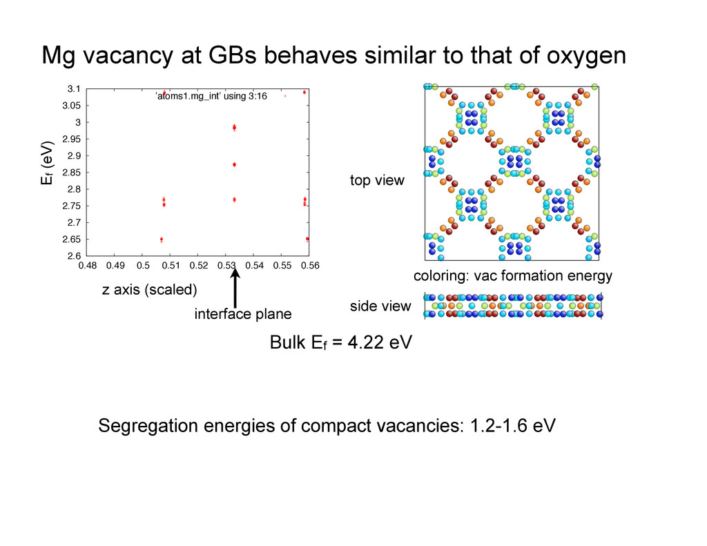
Ef (eV) top view side view coloring: vac formation energy 2.6 2.65 2.7 2.75 2.8 2.85 2.9 2.95 3 3.05 3.1 0.48 0.49 0.5 0.51 0.52 0.53 0.54 0.55 0.56 ’atoms1.mg_int’ using 3:16 Bulk Ef = 4.22 eV interface plane z axis (scaled) Segregation energies of compact vacancies: 1.2-1.6 eV
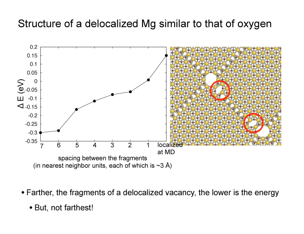
-0.35 -0.3 -0.25 -0.2 -0.15 -0.1 -0.05 0 0.05 0.1 0.15 0.2 0 1 2 3 4 5 6 7 • Farther, the fragments of a delocalized vacancy, the lower is the energy • But, not farthest! Δ E (eV) spacing between the fragments (in nearest neighbor units, each of which is ~3 Å) 1 2 3 4 5 6 localized at MD 7
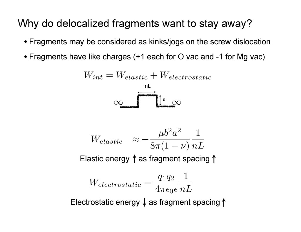
= W elastic + W electrostatic nL a 1 1 W elastic ⇡ µb2a2 8⇡(1 ⌫) 1 nL W electrostatic ⇡ q1q2 4⇡✏0 1 nL Elastic energy as fragment spacing W electrostatic = q1q2 4⇡✏0✏ 1 nL Electrostatic energy as fragment spacing • Fragments may be considered as kinks/jogs on the screw dislocation • Fragments have like charges (+1 each for O vac and -1 for Mg vac)
= q1q2 4⇡✏0✏ 1 nL W electrostatic = 0.606 n W elastic ⇡ µb2a2 8⇡(1 ⌫) 1 nL W electrostatic ⇡ q1q2 4⇡✏0 1 nL eV eV n - number of nearest neighbors nL a 1 1 a0 = 4.212˚ A b = a0 p 2 a = a0 2 µ = 132 141GPa ⌫ = 0.32 L = b q1, q2 = 1e ✏0 = 8.85 ⇥ 10 12Ohm 1m 1 ✏ this model = 7.92 Welastic = 0.63 0.68 n • Assumptions for elastic interactions perhaps incorrect (“a”, for example) • Analytical model may be corrected study kink/jog on a bulk dislocation Why do delocalized fragments want to stay away?
-1.2 -1 -0.8 -0.6 -0.4 -0.2 0 0 1 2 3 4 5 6 spacing between vacancy fragments • Contribution to energy due to other factors atoms colored by number of neighbors
methods 2. Ground-state structures of GBs 3. Structure and energetics of a vacancy at GBs • compact and delocalized vacancies 4. Transport of vacancies • observations and postulated mechanisms
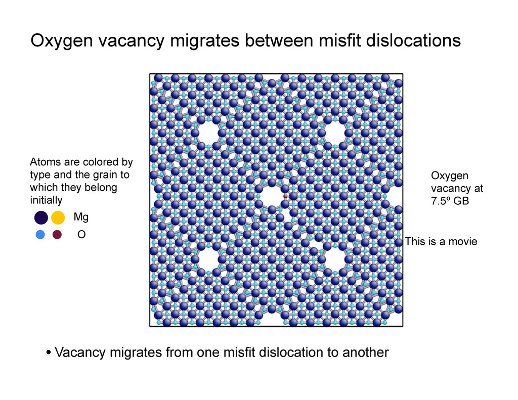
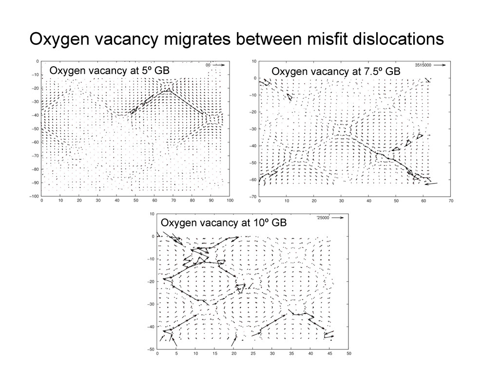
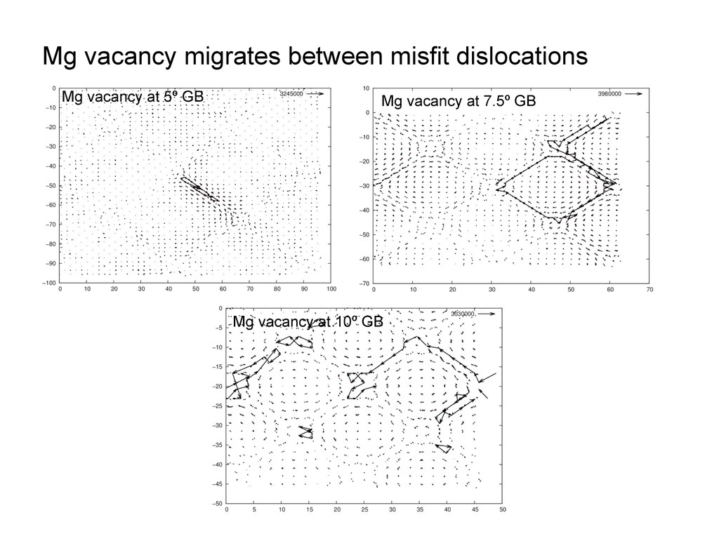
GB • Vacancy migrates from one misfit dislocation to another This is a movie Atoms are colored by type and the grain to which they belong initially Mg O
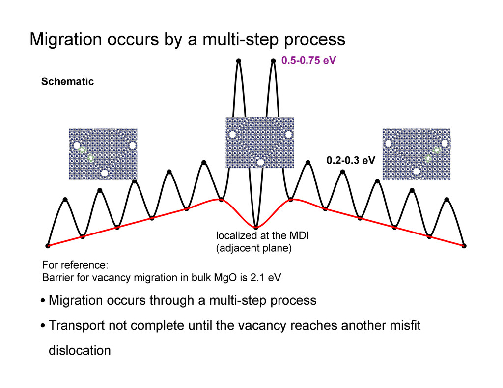
misfit dislocation to another • first by localizing at the MDI (usually at adjacent planes) • then by delocalizing again at the interface plane misfit dislocation t0 t0 +4 ps t0 +8 ps at adjacent plane defect at interface plane at interface plane (a) (b) (c)
MDI (adjacent plane) 0.2-0.3 eV 0.5-0.75 eV • Migration occurs through a multi-step process • Transport not complete until the vacancy reaches another misfit dislocation Schematic For reference: Barrier for vacancy migration in bulk MgO is 2.1 eV
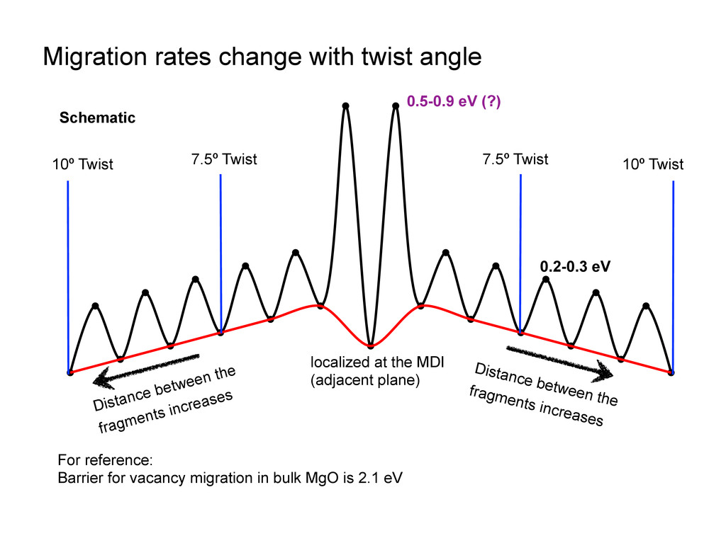
MDI (adjacent plane) Distance between the fragments increases 7.5º Twist 10º Twist 7.5º Twist 10º Twist 0.2-0.3 eV 0.5-0.9 eV (?) Distance between the fragments increases Schematic For reference: Barrier for vacancy migration in bulk MgO is 2.1 eV
boundaries are traps to vacancies of either species • Several metastable states for vacancy to reside at the grain boundary • In their lowest energy, they delocalize at misfit dislocations • They migrate from one misfit dislocation to another – In their intermediate, they localize in the vicinity of MDI