M. J. Demkowicz and B. Uberuaga Financial Support: Center for Materials at Irradiation and Mechanical Extremes (CMIME) at LANL, an Energy Frontier Research Center (EFRC) funded by U.S. Department of Energy, Office of Science, Office of Basic Energy Sciences Acknowledgments: R. G. Hoagland, J. P. Hirth, A. Kashinath, A. Vattré, X.-Y. Liu, A. Misra, and A. Caro
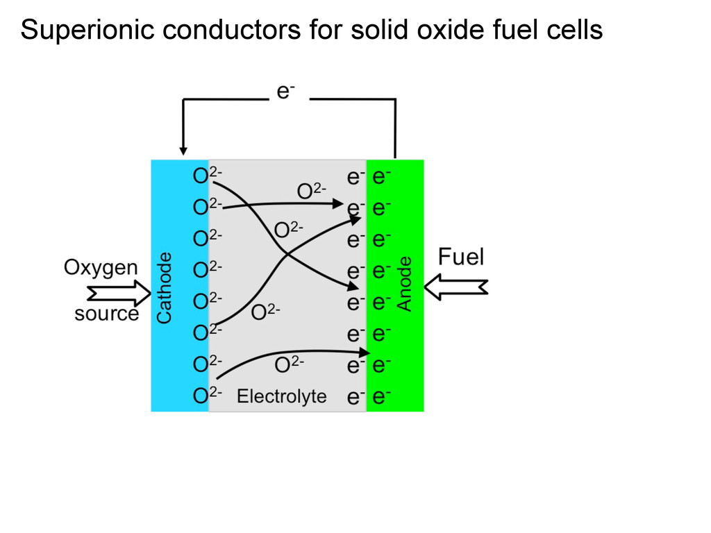
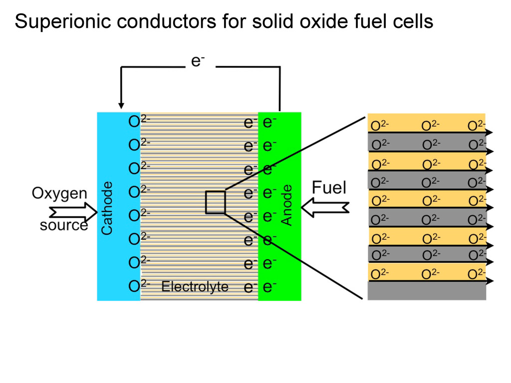
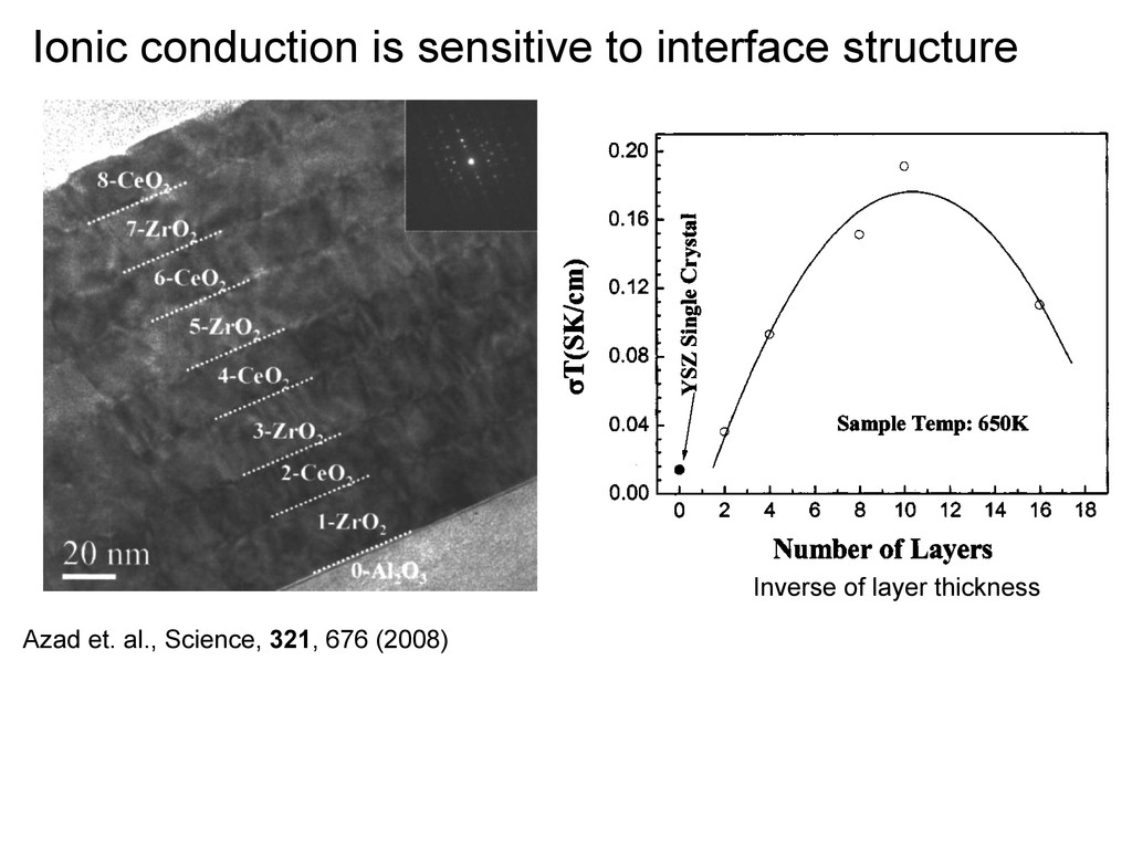
STO lattice. Because the bulk lattice constants of STO and YSZ are frequency plots. In the presence of blocking effects due to grain boundaries or electrodes, a further Fig. 1. (A) Z-contrast scanning transmission electron microscopy (STEM) image of the STO/YSZ interface of the [YSZ1nm /STO10nm ]9 superlattice (with nine repeats), obtained in the VG Microscopes HB603U microscope. A yellow arrow marks the position of the YSZ layer. (Inset) Low-magnification image obtained in the VG Microscopes HB501UX column. In both cases a white arrow indicates the growth direction. (B) EEL spectra showing the O K edge obtained from the STO unit cell at the interface plane (red circles) and 4.5 nm into the STO layer (black squares). (Inset) Ti L2,3 edges for the same positions, same color code. All spectra are the result of averaging four individual spectra at these positions, with an acquisition time of 3 s each. Fig. 2. Real part of the lateral electrical conductivity versus fre- on September 17, 2011 www.sciencemag.org Downloaded from by in ee ues in his to gi- is he is gle eas gle ior ers ler yer out dc ses he ses va- of are ors with the thickness of the YSZ, shows that the large conductivity values in these heterostructures orig- degraded interface structure when the YSZ layers exceed the critical thickness. Fig. 3. Dependence of the logarithm of the long-range ionic conductivity of the trilayers STO/YSZ/STO versus inverse temperature. The thickness range of the YSZ layer is 1 to 62 nm. Also included are the data of a single crystal (sc) of YSZ and a thin film (tf) 700 nm thick [taken from (7)] with the same nominal composition. (Top inset) 400 K conductance of [YSZ1nm /STO10nm ](ni/2) superlattices as a function of the number of interfaces, ni . (Bottom inset) Dependence of the conduct- ance of [STO10nm /YSZXnm /STO10nm ] trilayers at 500 K on YSZ layer thickness. Error bars are according to a 1 nS uncertainty of the con- ductance measurement. J. Garcia-Barriocanal et. al., Science, 321, 676 (2008) Why? • High defect concentrations • Faster transport due to interface structure; Strain-enhanced diffusion • No space charge in this example but possible in other interfaces 1.1 1 0.6 1
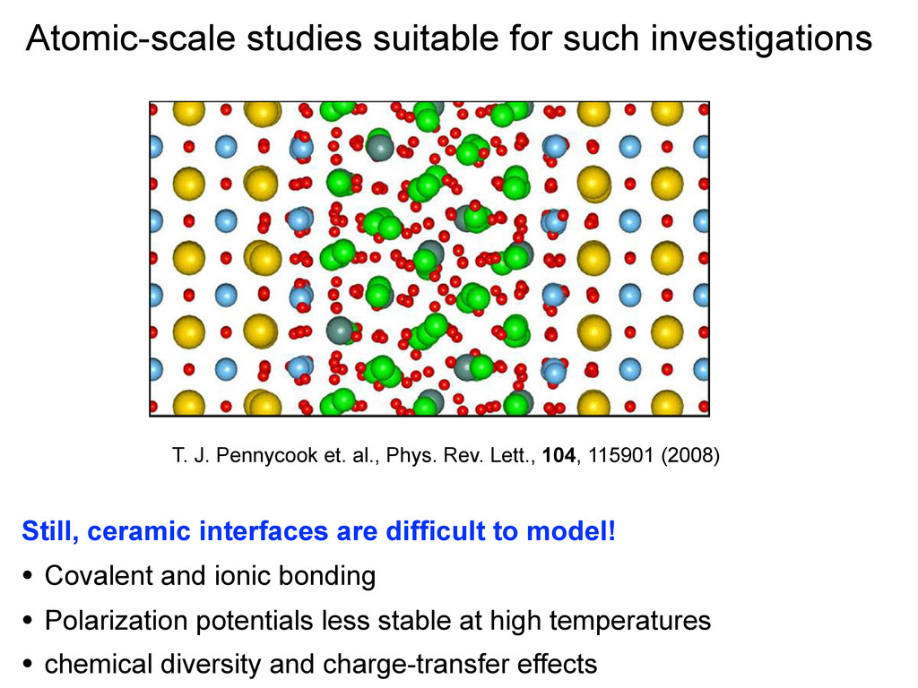
in the density and the fact that the charge on the ions is ill-defined. We can, however, estimate the effective magnitude by evaluating the ratio of the ime set) near FIG. 3 (color online). Structure of the 1 nm YSZ layer sand- wiched between layers of STO at 360 K. Sr atoms are shown as large yellow balls, Ti in blue, Zr in green, Y in gray, and O in red. R E V I E W L E T T E R S week ending 19 MARCH 2010 T. J. Pennycook et. al., Phys. Rev. Lett., 104, 115901 (2008) Still, ceramic interfaces are difficult to model! • Covalent and ionic bonding • Polarization potentials less stable at high temperatures • chemical diversity and charge-transfer effects
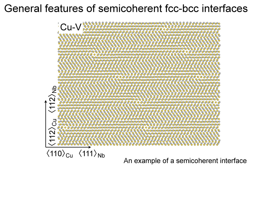
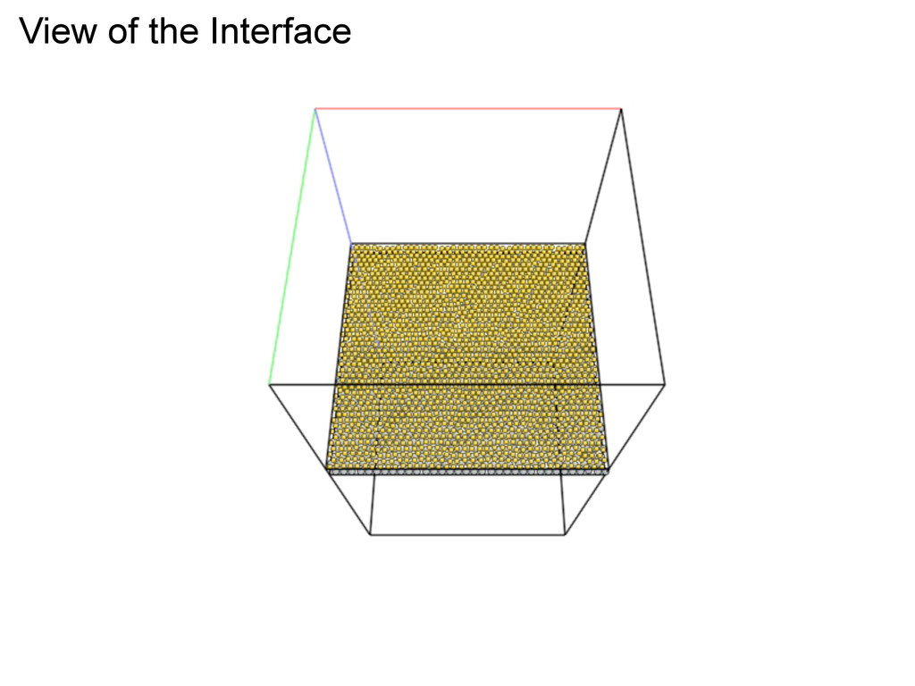
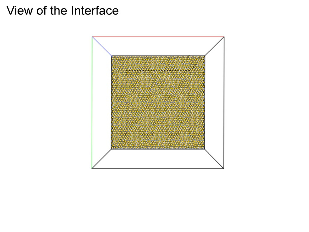
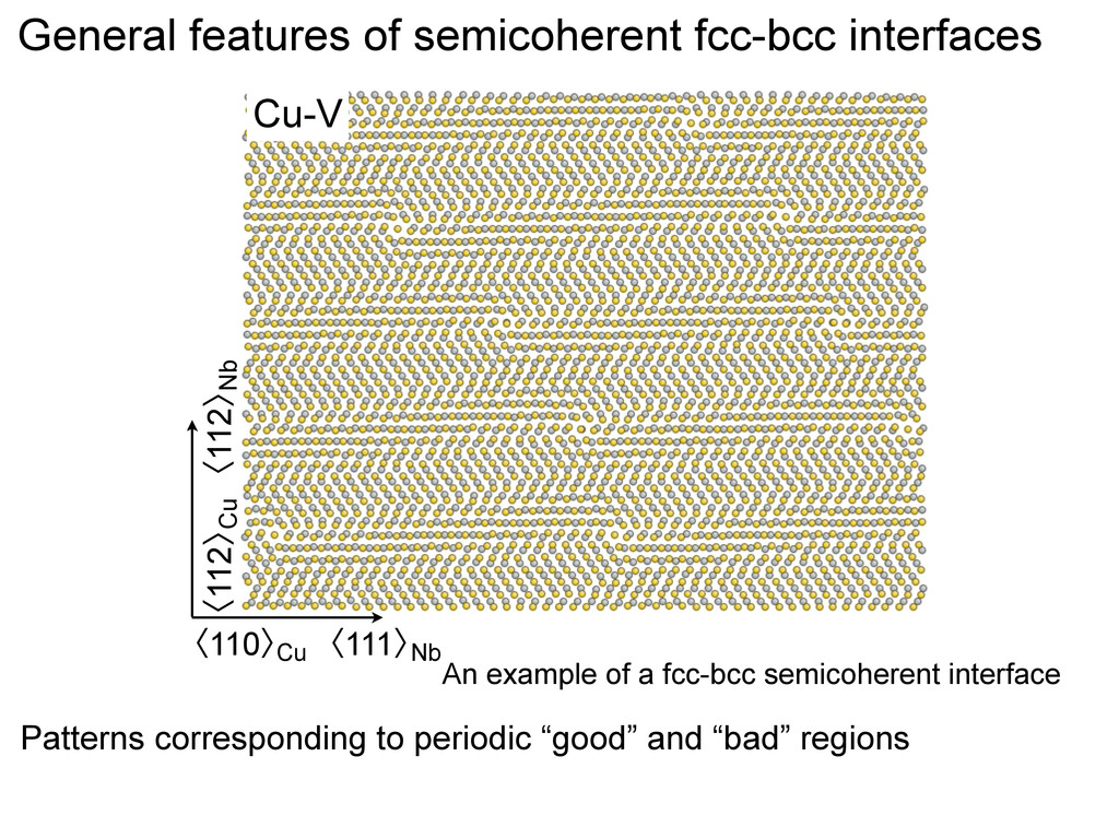
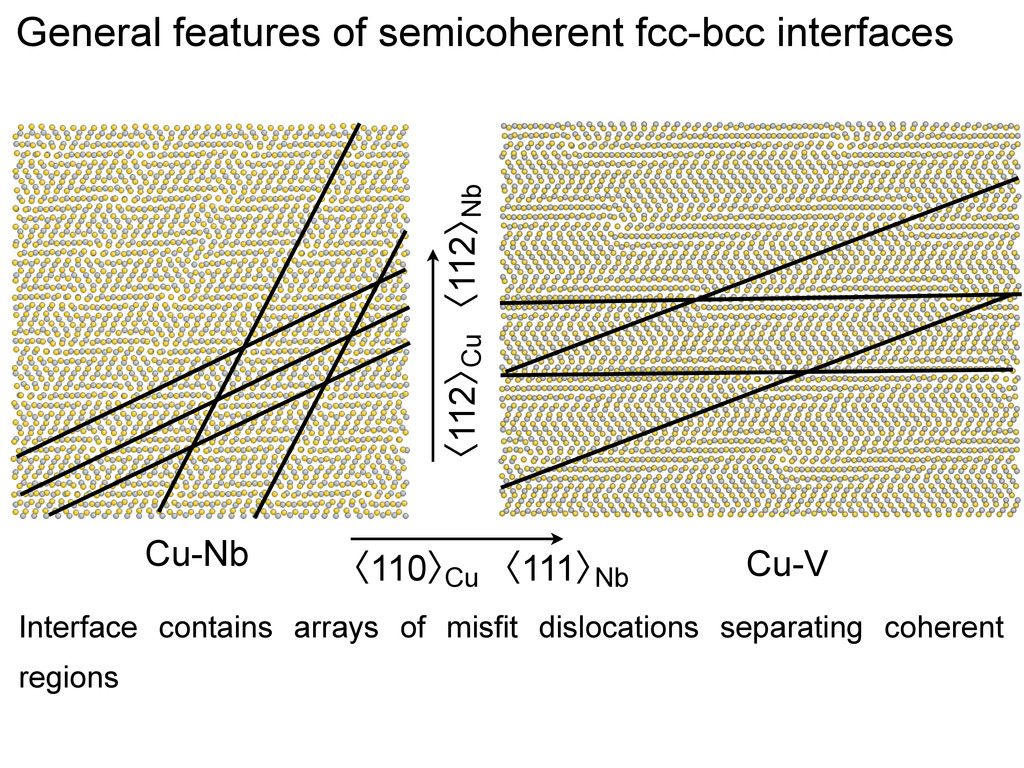
exist for metallic systems • less difficult - can probe the effect of structure on mass transport • Initial focus on • interfaces of immiscible fcc-bcc semicoherent metal systems Cu-Nb, Cu-V, Cu-Mo, Cu-Fe, and Ag-V (111) fcc (110) bcc || ʪ110ʫ fcc ʪ111ʫ bcc || and Kurdjumov-Sachs (KS): (111) fcc (110) bcc || ʪ110ʫ fcc ʪ100ʫ bcc || and Nishiyama-Wassermann (NW): Motivated by experiments A. Misra et al., JOM, Sept, 62 (2007) Interfaces act as obstacles to slip and sinks for radiation-induced defects. Hence, nanolayered composites that contain a large volume fraction of inter- faces provide over an order of magnitude increase in strength and enhanced radia- tion damage tolerance compared to bulk materials. This paper shows the experi- mental and atomistic modeling results from a Cu-Nb nanolayered composite to highlight the roles of nanostructur- ing length scales and the response of interfaces to ion collision cascades in designing composite materials with high radiation damage tolerance. INTRODUCTION The performance of materials in extreme environments of irradiation and temperature must be signifi cantly improved to extend the reliability, life- time, and effi ciency of future nuclear reactors.1 In reactor environments, damage introduced in the form of radia- The Radiation Damage Tole of Ultra-High Strength Nan Composites A. Misra, M.J. Demkowicz, X. Zhang, and R.G. Hoagland interfaces are to act as sinks for radia- tion-induced defects. Studies conducted on sputter-deposited Cu-Nb multilayers b a 150 keV He, 1017 cm-2, 300 K After He implantation
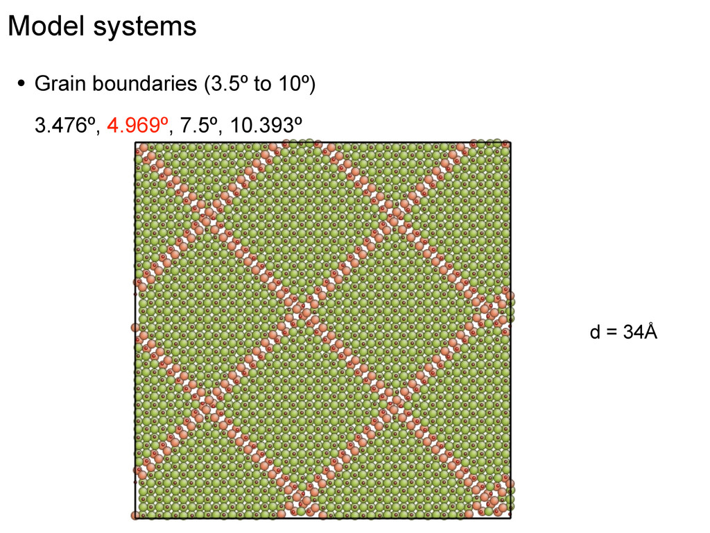
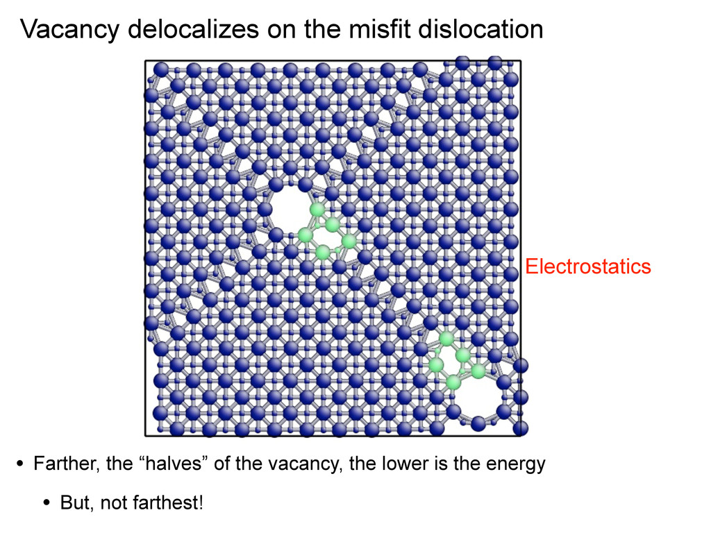
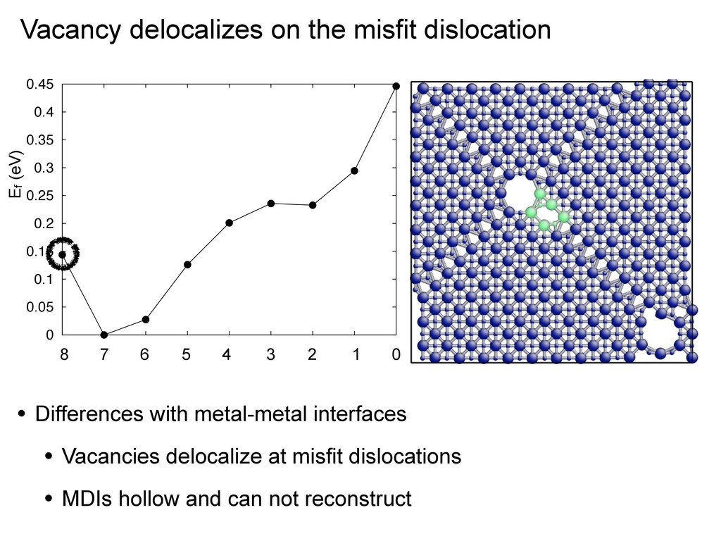
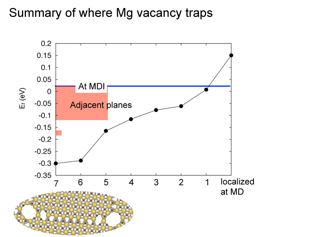
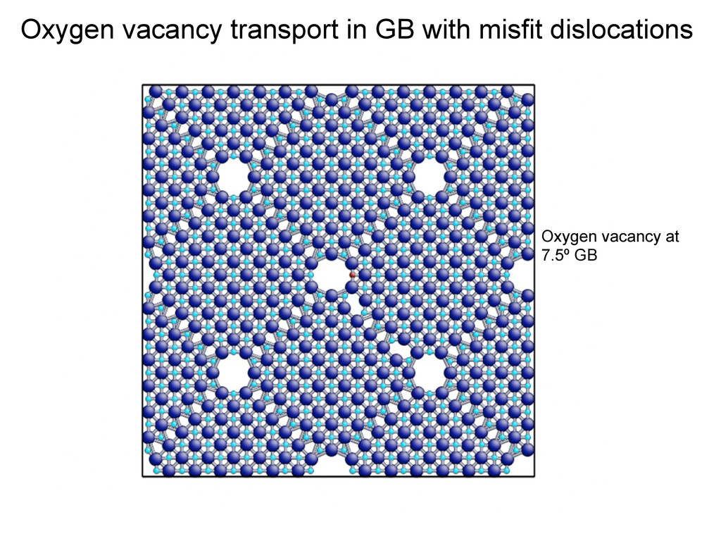
defects at semicoherent interfaces • Migration of point defects and relation to the interface structure • Implications to ceramic interfaces • case of MgO grain boundaries
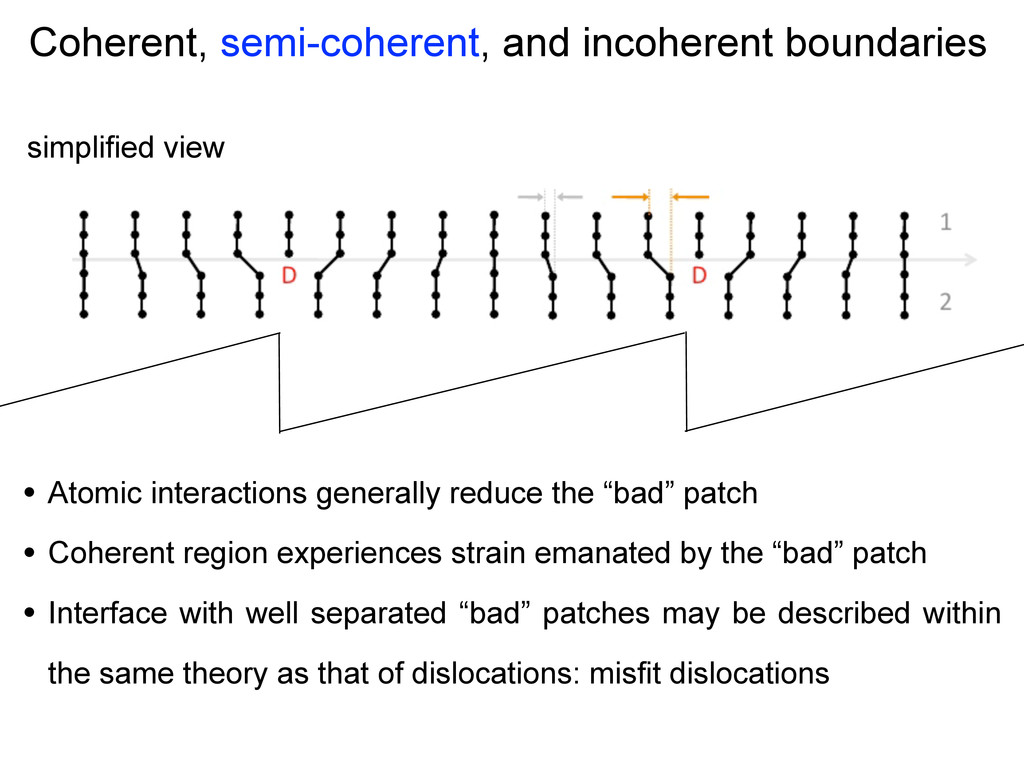
generally reduce the “bad” patch • Coherent region experiences strain emanated by the “bad” patch • Interface with well separated “bad” patches may be described within the same theory as that of dislocations: misfit dislocations
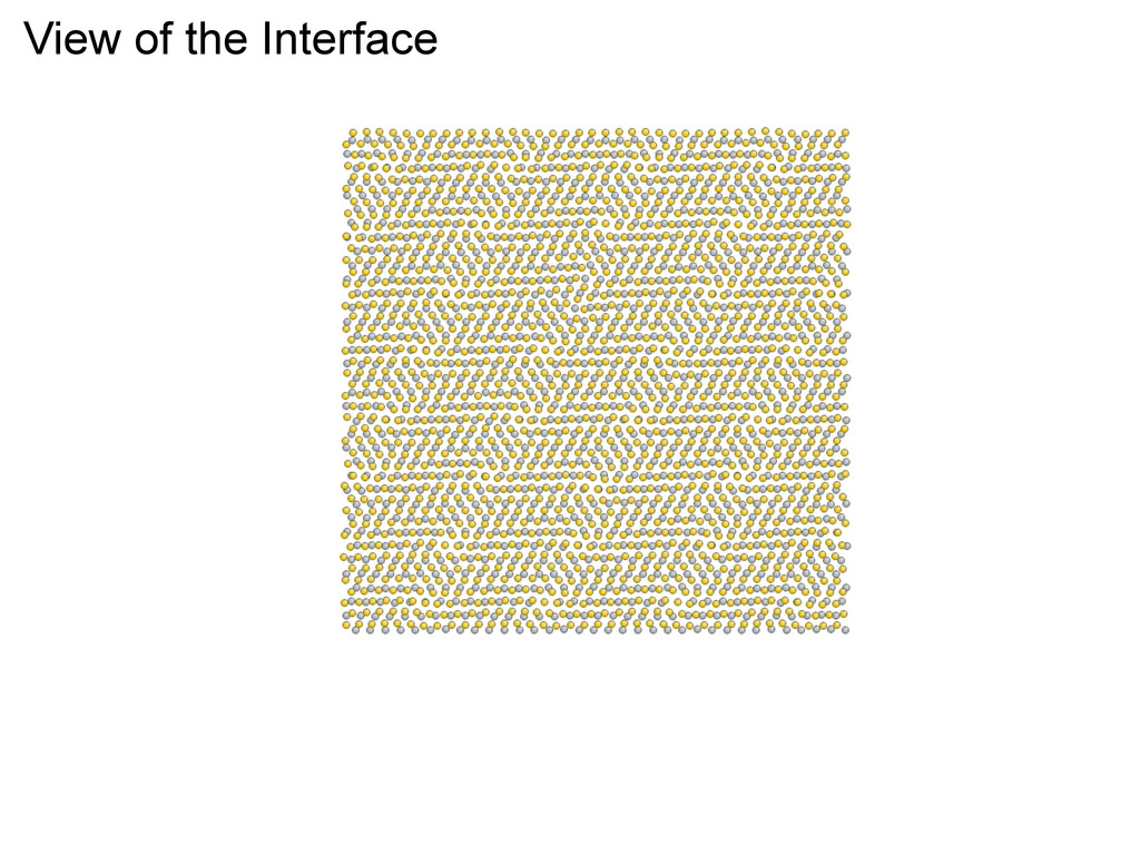
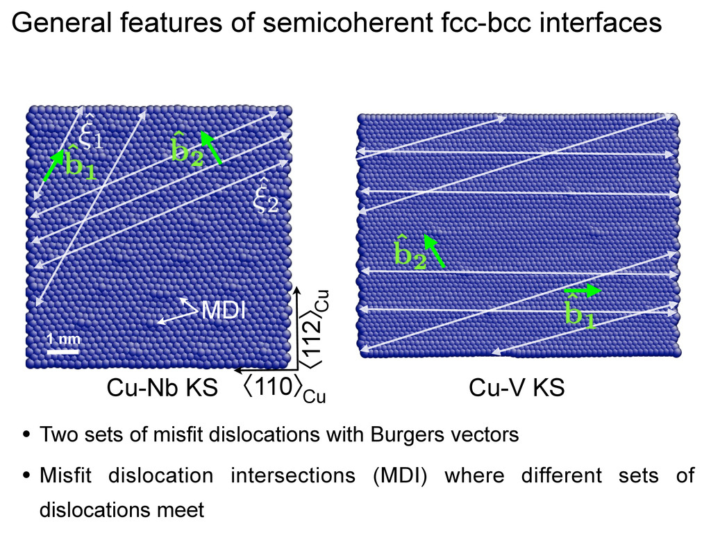
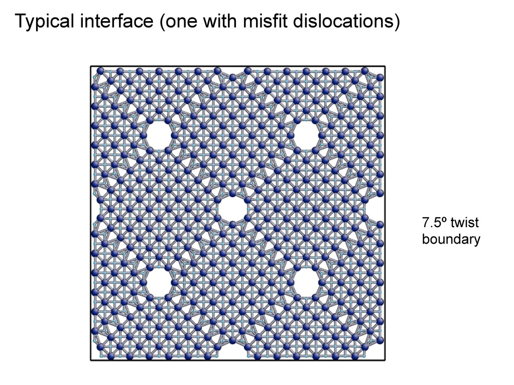
MDI • Two sets of misfit dislocations with Burgers vectors • Misfit dislocation intersections (MDI) where different sets of dislocations meet General features of semicoherent fcc-bcc interfaces
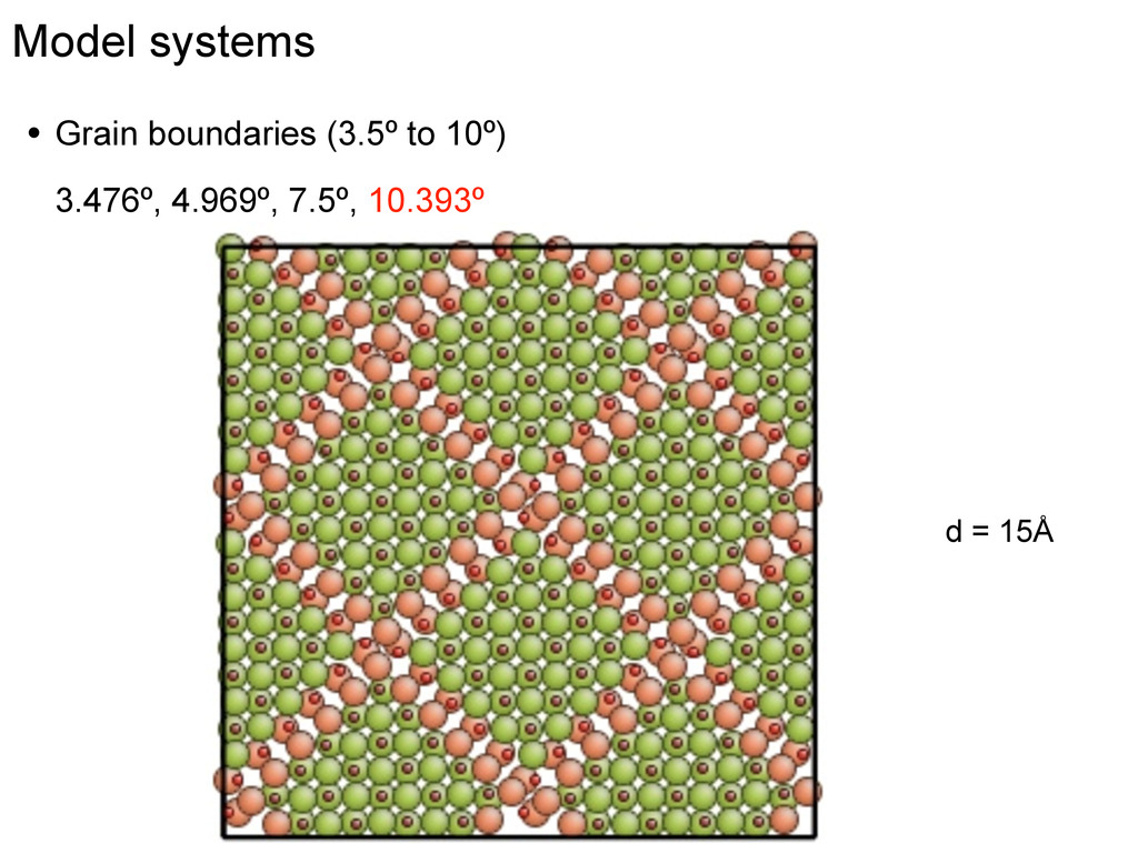
defects at semicoherent interfaces • Migration of point defects and relation to the interface structure • Implications to ceramic interfaces • case of MgO grain boundaries
defects at semicoherent interfaces • Migration of point defects and relation to the interface structure • Implications to ceramic interfaces • case of MgO grain boundaries
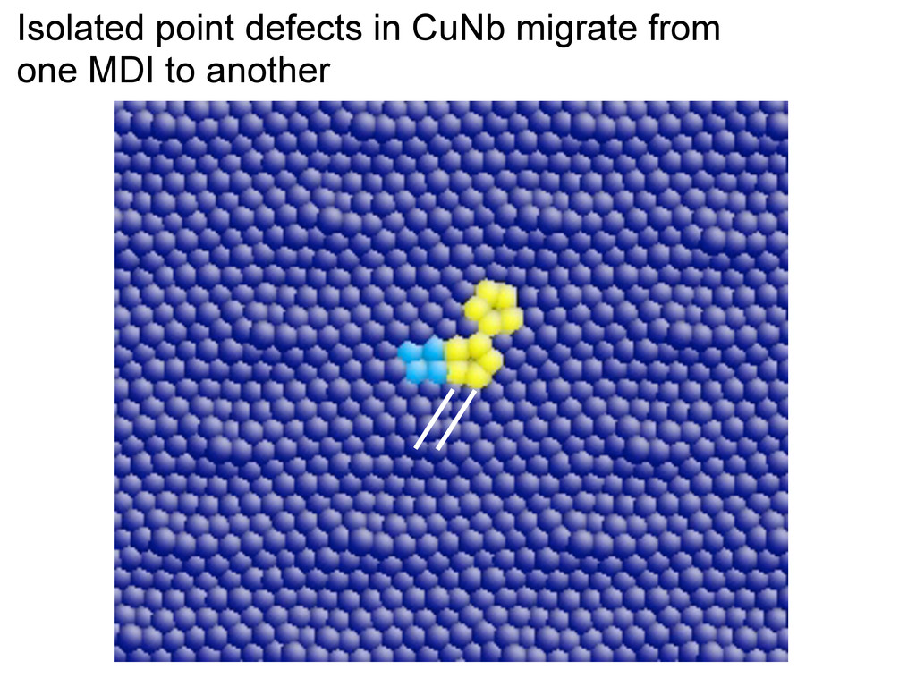
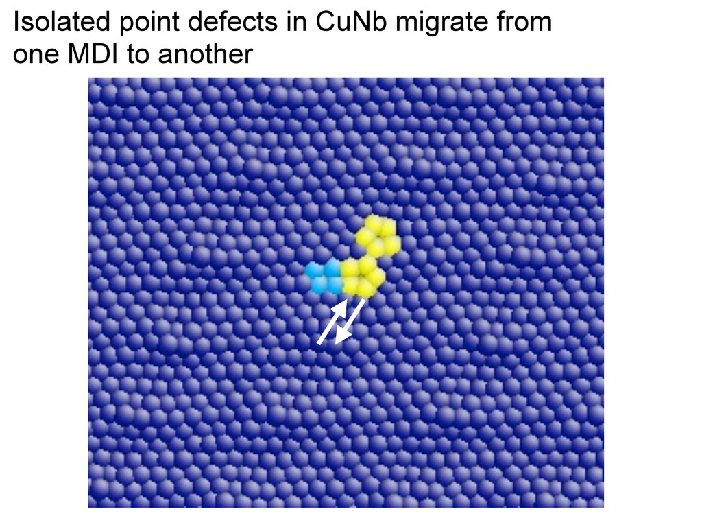
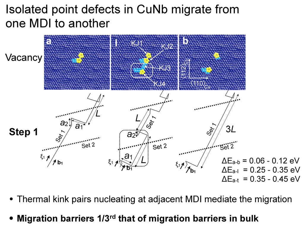
screw • In the intermediate step, the point defect is delocalized on two MDI Vacancy Interstitial Point defects migrate from one MDI to another in CuNb
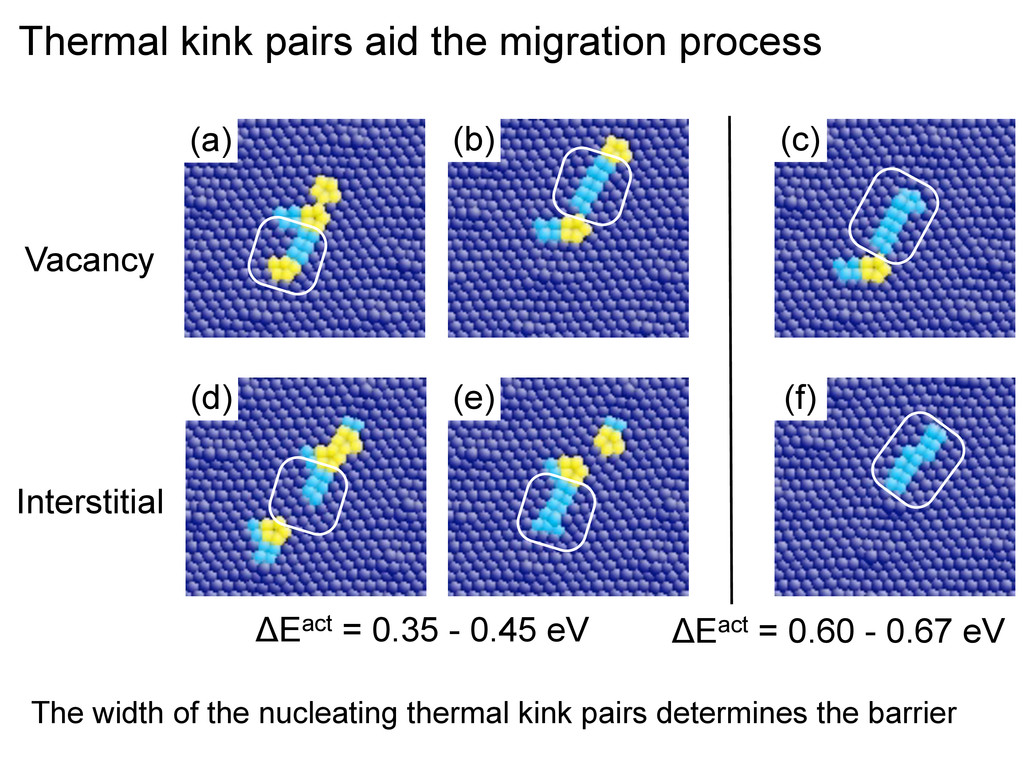
1 Set 2 a1 a2 L L b1 !1 b1 !1 Set 1 Set 2 3L • Thermal kink pairs nucleating at adjacent MDI mediate the migration • Migration barriers 1/3rd that of migration barriers in bulk KJ1 KJ3´ KJ4 Cu ʪ112ʫ ʪ110ʫ Cu KJ2´ KJ4 KJ3 KJ2 KJ1 Cu ʪ112ʫ ʪ110ʫ Cu a b I Vacancy Step 1 ! (reaction coordinate) t a I t t b " E (eV) 0 0.05 0.1 0.15 0.2 0.25 0.3 0.35 0.4 0.45 0 0.1 0.2 0.3 0.4 0.5 0.6 0.7 0.8 0. t I t b t "Ea-b = 0.06 - 0.12 eV "Ea-I = 0.25 - 0.35 eV "Ea-t = 0.35 - 0.45 eV Vacancy Interstitial Isolated point defects in CuNb migrate from one MDI to another
1 Set 2 a1 a2 L L b1 !1 b1 !1 Set 1 Set 2 3L KJ1 KJ3´ KJ4 Cu ʪ112ʫ ʪ110ʫ Cu KJ2´ KJ4 KJ3 KJ2 KJ1 Cu ʪ112ʫ ʪ110ʫ Cu a b I Vacancy Step 1 ! (reaction coordinate) t a I t t b " E (eV) 0 0.05 0.1 0.15 0.2 0.25 0.3 0.35 0.4 0.45 0 0.1 0.2 0.3 0.4 0.5 0.6 0.7 0.8 0. t I t b t "Ea-b = 0.06 - 0.12 eV "Ea-I = 0.25 - 0.35 eV "Ea-t = 0.35 - 0.45 eV Vacancy Interstitial Isolated point defects in CuNb migrate from one MDI to another • Thermal kink pairs nucleating at adjacent MDI mediate the migration • Migration barriers 1/3rd that of migration barriers in bulk
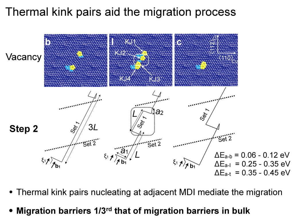
b1 !1 Set 1 Set 2 b1 !1 Set 1 Set 2 3L KJ1 KJ3´ KJ4 KJ2´ Cu ʪ112ʫ ʪ110ʫ Cu c b I Vacancy Step 2 ! (reaction coordinate) t a I t t b " E (eV) 0 0.05 0.1 0.15 0.2 0.25 0.3 0.35 0.4 0.45 0 0.1 0.2 0.3 0.4 0.5 0.6 0.7 0.8 0. t I t b t "Ea-b = 0.06 - 0.12 eV "Ea-I = 0.25 - 0.35 eV "Ea-t = 0.35 - 0.45 eV Vacancy Interstitial Thermal kink pairs aid the migration process • Thermal kink pairs nucleating at adjacent MDI mediate the migration • Migration barriers 1/3rd that of migration barriers in bulk
all intermediate states need to be visited in every migration • The underlying physical phenomenon, however, remains unchanged ! (reaction coordinate) t a I t t b " E (eV) 0 0.05 0.1 0.15 0.2 0.25 0.3 0.35 0.4 0.45 0 0.1 0.2 0.3 0.4 0.5 0.6 0.7 0.8 0. t I t b t "Ea-b = 0.06 - 0.12 eV "Ea-I = 0.25 - 0.35 eV "Ea-t = 0.35 - 0.45 eV Vacancy Interstitial
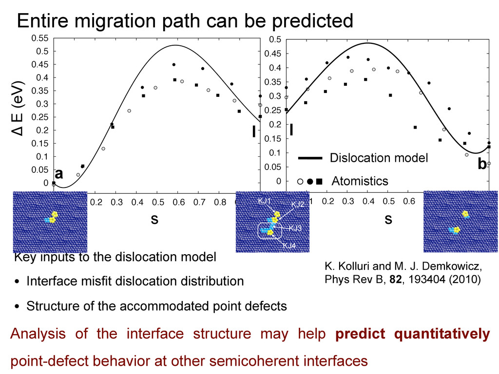
dislocation model • Interface misfit dislocation distribution • Structure of the accommodated point defects Analysis of the interface structure may help predict quantitatively point-defect behavior at other semicoherent interfaces Δ E (eV) s s 0 0.05 0.1 0.15 0.2 0.25 0.3 0.35 0.4 0.45 0.5 0.55 0 0.1 0.2 0.3 0.4 0.5 0.6 0.7 0.8 0.9 1 I a 0 0.05 0.1 0.15 0.2 0.25 0.3 0.35 0.4 0.45 0.5 0 0.1 0.2 0.3 0.4 0.5 0.6 0.7 0.8 0.9 1 b I Dislocation model Atomistics K. Kolluri and M. J. Demkowicz, Phys Rev B, 82, 193404 (2010) KJ1 KJ3´ KJ4 Cu ʪ112ʫ ʪ110ʫ Cu KJ2´ KJ4 KJ3 KJ2 KJ1
constant for all states in our dislocation model [and therefore does not appear in Eq. (1)], actually varies along the direct migration path. To estimate the core energy of the kink-jog, we summed differences in atomic energies between the core atoms and corresponding atoms in a defect- free interface. The kink-jog core is taken to consist of 19 atoms: the 5-atom ring in the Cu terminal plane and the 7 neighboring Cu and Nb atoms from each of the two planes adjacent to the Cu terminal plane. Core volumes were computed in an analogous way. The core energies of the migrating jog are plotted as filled triangles in Fig. 15(a) and are in good semiquantitative agreement with the overall energy changes occurring along the direct migration path. Core volumes are plotted as filled circles. Figure 15(b) shows the Cu and Nb interface planes with a point defect in the extended state B. Arrows mark the locations of the two kink-jogs and red lines mark the nominal locations of set 2 misfit dislocation cores. The numbers are TABLE I. Transitions occurring during migration of individual point defects that were considered in kMC simulations, their corresponding activation energy barriers, and number of distinct end states for a given start state. Transition Activation energy Number of type (eV) distinct end states A → I 0.40 2 A → B 0.40 2 I(near A) → B 0.15 1 I(near A) → A 0.15 1 B → A 0.35 1 B → I 0.35 2 B → I 0.20 1 B → C 0.35 1 I(near C) → C 0.15 1 I(near C) → B 0.15 1 I → B 0.15 1 205416-9 • Hypothesis: • transition state theory is valid and • Rate-limiting step will determine the migration rate ≥ 0.4 eV • Validation: • kinetic Monte Carlo (since the migration path is not trivial) • Statistics from molecular dynamics
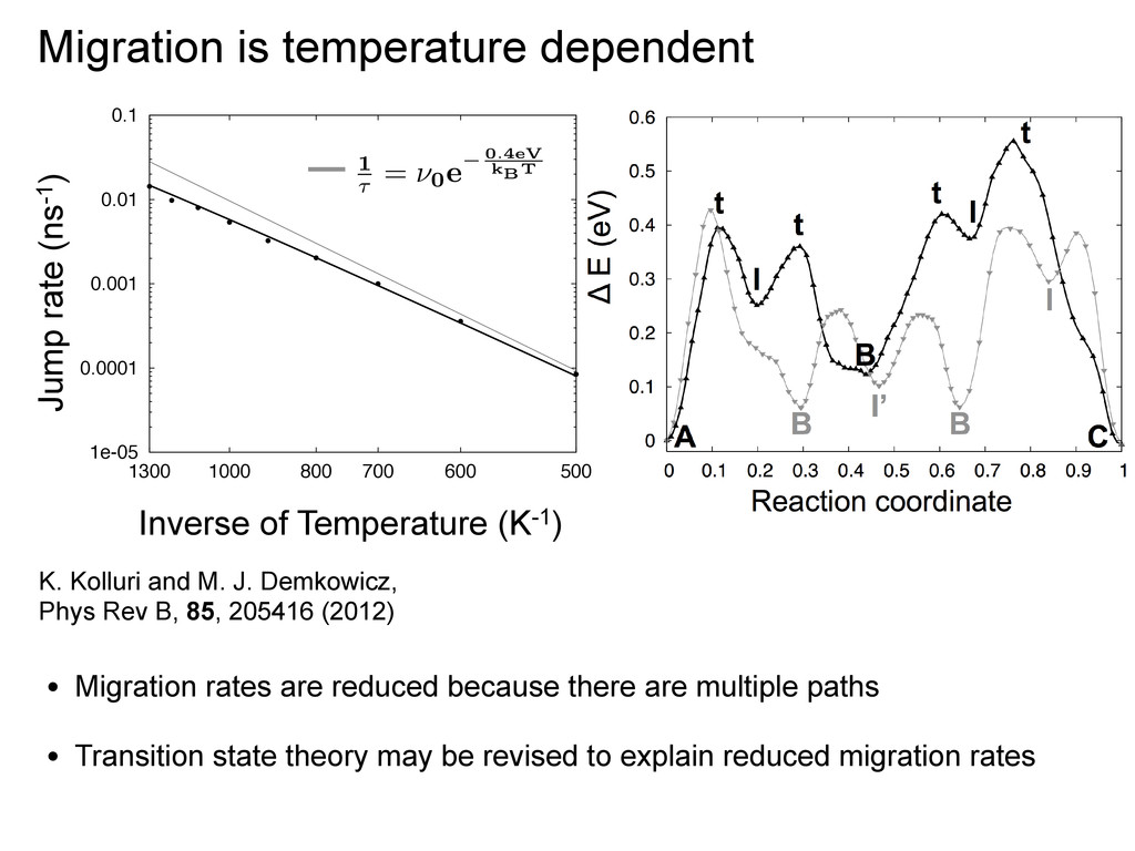
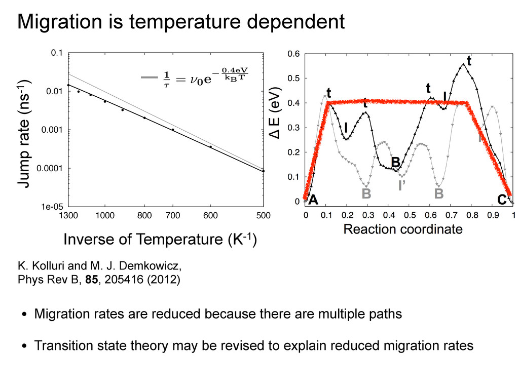
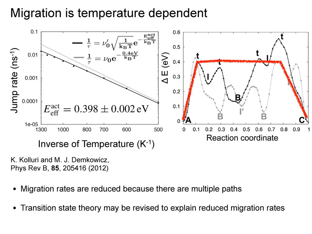
0.0001 0.001 0.01 0.1 1300 1000 800 700 600 500 Inverse of Temperature (K-1) • Migration rates are reduced because there are multiple paths • Transition state theory may be revised to explain reduced migration rates Migration is temperature dependent K. Kolluri and M. J. Demkowicz, Phys Rev B, 85, 205416 (2012)
800 700 600 500 Inverse of Temperature (K-1) Migration is temperature dependent 1 = 0 e 0.4eV kBT • Migration rates are reduced because there are multiple paths • Transition state theory may be revised to explain reduced migration rates K. Kolluri and M. J. Demkowicz, Phys Rev B, 85, 205416 (2012)
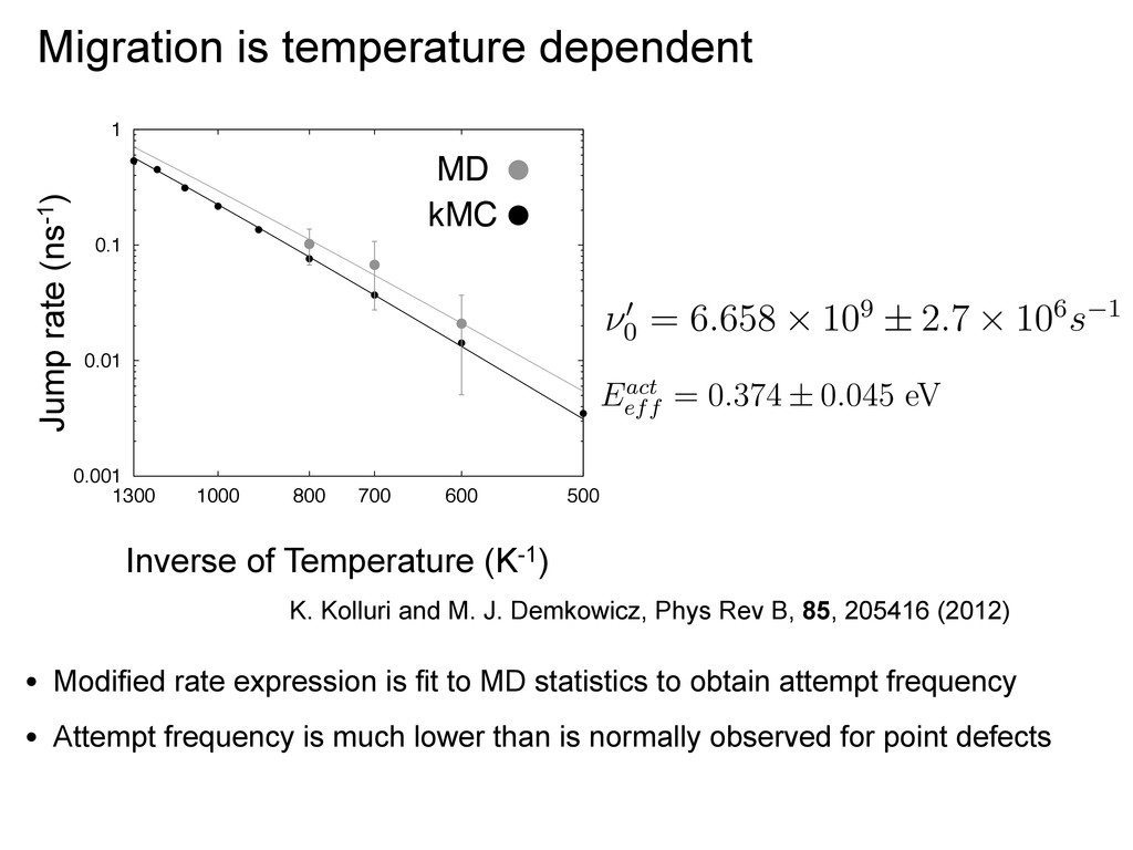
Eact e kBT 1 = 0 e 0.4eV kBT 1e-05 0.0001 0.001 0.01 0.1 1300 1000 800 700 600 500 Inverse of Temperature (K-1) Migration is temperature dependent ln[(s!)p(t/τ,s)] = s ln(t/τ) − t/τ. (10) s are obtained for all three temperatures, confirming tion that point defect migration follows a Poisson ig. 17). The jump rates for each temperature, y fitting, are plotted in Fig. 16(b) as filled gray h uncertainties corresponding to the error in the es fit. The gray line is the least-squares fit of Eq. (8) obtained from MD. The activation energy obtained MC model (Eact eff = 0.398 ± 0.002 eV) is well within nty of the activation energy found by fitting the MD y, Eact eff = 0.374 ± 0.045 eV. ctive attempt frequency for defect migration ob- fitting the MD data is ν0 = 6.658 × 10⁹ ± 2.7 × is value is several orders of magnitude lower than mpt frequencies for point defect migration in fcc , 1012−1014 s−1.72–74 A mechanistic interpretation ow migration attempt frequency is not immediately g. One possible explanation is that it arises from number of atoms participating in the migration • Migration rates are reduced because there are multiple paths • Transition state theory may be revised to explain reduced migration rates K. Kolluri and M. J. Demkowicz, Phys Rev B, 85, 205416 (2012)
600 500 Jump rate (ns-1) Inverse of Temperature (K-1) Migration is temperature dependent • Modified rate expression is fit to MD statistics to obtain attempt frequency • Attempt frequency is much lower than is normally observed for point defects model( Eact eff = 0 . 398±0 . 002 eV) is w by fitting the MD data, namely Ea e ⌫ 0 0 = 6 . 658 ⇥ 109 ± 2 . 7 ⇥ 106 s 1 tained by fitting the MD data is ⌫ 0 0 of magnitude lower than typical at namely 1012 1014 s 1 69–71. A mec frequency is not immediately forth the large number of atoms particip for migration of compact point defe frequency because it involves the m model( Eact eff = 0 . 398±0 . 002 eV) is well wi by fitting the MD data, namely Eact eff = 0 Eact eff = 0 . 374 ± 0 . 045 eV ⌫ 0 0 = 6 . 658 ⇥ for defect migration obtained by fitting t value is several orders of magnitude lowe migration in fcc Cu, namely 1012 1014 low migration attempt frequency is not im is that it arises from the large number of attempt frequency for migration of compa der of the Einstein frequency because it i K. Kolluri and M. J. Demkowicz, Phys Rev B, 85, 205416 (2012)
sites –density of these sites depends on interface structure • Point defects migrate from trap to trap –migration is multi-step and involves concerted motion of atoms –migration can be analytically represented How much of this knowledge can be ported to ceramics? • Electrostatics • covalency • multiple species
sites –density of these sites depends on interface structure • Point defects migrate from trap to trap –migration is multi-step and involves concerted motion of atoms –migration can be analytically represented How much of this knowledge can be ported to ceramics? • Electrostatics : MgO - highly ionic and simple to model • covalency • multiple species
using the simplest of ionic potentials available • Fixed charge on each atom (this potential has full charge) • Molecular statics and dynamics (at 2000K) <100> <100> +ø/2 Eij = Ae rij ⇢ C r6 ij + Cqiqj ✏rij 1
nL a 1 1 W elastic ⇡ µb2a2 8⇡(1 ⌫) 1 nL W electrostatic ⇡ q1q2 4⇡✏0 1 nL b = a0 p 2 a = a0 2 µ = 155 GPa ⌫ = 0.18 L = b q1, q2 = 1e ✏0 = 8.85e 12 Ohm 1m 1 a0 = 4.212˚ A W electrostatic = q1q2 4⇡✏0✏ 1 nL ✏ this model = 7.92 W electrostatic = 0.606 n Welastic = 0.63(0.68) n eV eV n - number of nearest neighbors 132-141 GPa 0.32 • Elastic energies are perhaps an overestimate!
these sites depends on interface structure • Point defects migrate from trap to trap –migration is multi-step and involves concerted motion of atoms –migration can be analytically represented Ceramics: • Defects trapped at and migrate from one misfit dislocation to another • Electrostatics in the model ceramics play greater role • Defects migrate faster and anisotropic
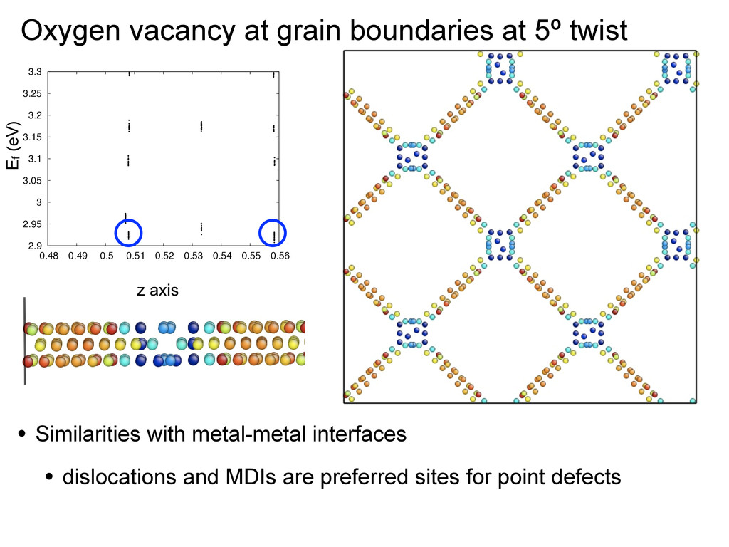
0.49 0.5 0.51 0.52 0.53 0.54 0.55 0.56 • Similarities with metal-metal interfaces • dislocations and MDIs are preferred sites for point defects Ef (eV) z axis Oxygen vacancy at grain boundaries at 5º twist
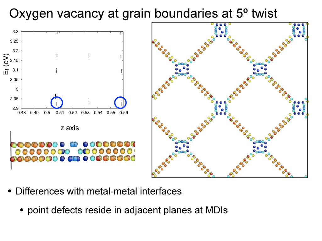
0.49 0.5 0.51 0.52 0.53 0.54 0.55 0.56 • Differences with metal-metal interfaces • point defects reside in adjacent planes at MDIs Ef (eV) z axis Oxygen vacancy at grain boundaries at 5º twist