Upgrade to Pro — share decks privately, control downloads, hide ads and more …

Scanning Tunnelling Microscopy - Master 2 SMNO Nanomat

jelledionot
December 07, 2011

Scanning Tunnelling Microscopy - Master 2 SMNO Nanomat

jelledionot

December 07, 2011
Tweet

More Decks by jelledionot

Other Decks in Education

Transcript

  1. Scanning Tunnelling Microscopy Report by Jelle Dionot Practical done with

    Marcel Br¨ andlein, under the supervision of Piotr Sleczkowski Universit´ e Pierre et Marie Curie Institut des Nanosciences de Paris Nanomat Master Program – Group 2 Wednesday, December 7th 2011
  2. Contents Introduction 1 1 Basic principles 1 1.1 Theoretical background

    . . . . . . . . . . . . . . . . . . . . . . . . . . . . . 1 1.2 Experimental aspects . . . . . . . . . . . . . . . . . . . . . . . . . . . . . . 2 2 Results and discussions 3 2.1 First acquisitions and influence of the scanning parameters . . . . . . . . . 3 2.2 Drift: a vexing problem . . . . . . . . . . . . . . . . . . . . . . . . . . . . . 4 2.3 Higher resolution images . . . . . . . . . . . . . . . . . . . . . . . . . . . . 6 2.4 Commensurability of the adsorbate . . . . . . . . . . . . . . . . . . . . . . 7 Conclusion 9
  3. Introduction Only thirty years ago, G. Binning, H. Rohrer et

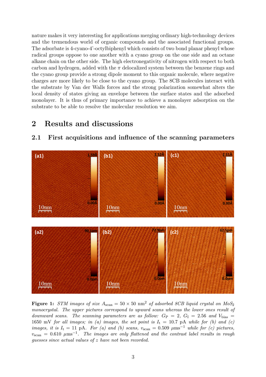
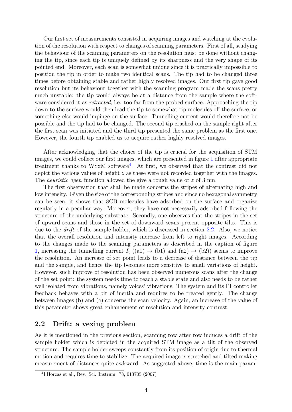
    al. reported the first observation of the quantum mechanical tunnelling current through vacuum1. Based on this effect, experi- mental set-ups were elaborated to measure the small variations of current and therefore probe the electronic density of a material surface, giving birth to the so-called scanning tunnelling microscopy (STM). Even though this technique can be very cumbersome to master finely, it is about to reach a state-of-the-art in such a way that atomic resolution and functional observations can quite easily be done. In this report, we present the basic principles of this technique and the analysis of the interface between an MoS2 monocrystal surface covered by 8CB liquid crystal and a model for the adsorption geometry of this organic compound on the hexagonal substrate, based on the study of the obtained STM images. 1 Basic principles 1.1 Theoretical background Considering free electrons as plane waves ψ propagating along the z-direction, quantum mechanics predict that in the presence of a uniform, finite but infinitely long step potential V0 , the plane waves are non-zero into the barrier, which is unexpected from a classical point of view. The electron wavefunction inside the potential barrier is indeed exponentially damped as it propagates, such that: ψ(z) = A · T · e−κz with κ = 2m(V0 − E) 2 (1) In the above equation, T is the transmission coefficient and A is a normalization constant. For z going to infinity, the wavefunction is damped down to zero. But for a potential barrier of finite thickness d, electrons with kinetic energy smaller than V0 can still and all overcome the barrier, depending on the thickness. Indeed, two metallic planes separated by a small distance d = z2 −z1 can represent such a described system, in which the gap between the plates represent the potential barrier. This potential V0 (z) varies along z. Using the WKB2 approximation method, Schr¨ odinger equation is solved giving the following transmission coefficient for a particle tunnelling through a single potential barrier characterized by the so-called turning points z1 and z2 : T exp −2 z2 z1 κ(z)dz (2) According to the Landauer-B¨ uttiker formalism, the transmission coefficient is related to the tunnelling current such that the latter is proportional to the sum over all the transmission channels. However, in order to achieve a net current along one direction, a potential bias Vbias is applied so that the potential is higher on one side of the gap. The obtained tunnelling current reads: I = e π EF +eVbias EF T(E, d)dE (3) 1G. Binning, H. Rohrer, Ch. Gerber, E. Weibel, Appl. Phys. Lett. 40, 178 (1982) 2Wentzel–Kramers–Brillouin 1
  4. In this equation, one sees that firstly the tunnelling current

    and the distance between the two plates are coupled, and secondly it depends on the applied bias voltage. Fur- thermore, perturbation theory calculations can show that the derivative of the tunnelling current with respect to the applied bias is a function of the local density of states ρ at the surface of the metal, such that: dI(V ) dV ∝ ρ(r, EF + eV ) (4) The local density of states ρ is directly proportional to the atomic charge distribution and therefore the measure of the derivative of the tunnelling current gives great insight on the atoms occupying the probed surface. 1.2 Experimental aspects In practice, STM requires a metallic tip ideally sharp enough to be ended by a single atom, which represent half of the conductive material required for the tunnelling current to occur, the sample being the second half. An image of the surface is made thanks to a scanning of the tip on the surface, measuring the local density of states as expressed in equation 4. The resolution of the measurement depends on the quality of the tip. In our experiment, we use a Pt90 Ir10 wire of a fraction of a millimetre thick, which we cut at grazing angle with a pair of blunt scissors which literally rips a rather sharp tip off the wire. Platinum makes the tip extremely inert and resistant to corrosion and Iridium pro- vides stiffness for high sharpness. Such technique, when done correctly, provides similar results and resolution as compared to a tip made by chemical etching of tungsten. Based on the above theoretical aspects, tunnelling current is nowadays mainly manip- ulated within three experimental techniques. An STM image can be acquired through constant height method, constant current method and scanning tunnelling spectroscopy. Equation 4 displays the physical quantity involved in the latter mentioned technique, which consists in measuring the local density of state by measuring the variation of the current while tuning the bias voltage. However, for our purposes and within our STM experiment, the set-up keeps a constant current by constantly adjusting the distance be- tween the tip and the sample, thanks to a proportional-integral (PI ) controller. Any variation of the current encountered by the scanning tip is counterbalanced by a feedback process of the PI controller which changes the distance between the tip and the sample thanks to piezoelectric nanopositioners in order to keep the tunnelling current at a con- stant value which the operator specifies as the set point noted It . A two dimensional map of the local density of state is therefore obtained, giving insight on the surface profile. The resolution is improved iteratively by this feedback method which optimizes the involved parameters, such as the proportional and integral gains GP and GI . The STM image size is specified by Ascan and the speed of the scan by the scan velocity parameter vscan . Our sample consists of a MoS2 semiconductor substrate layered on a sample holder thanks to scotch tape method, on which a solution of 8CB is deposited. The substrate has an hexagonal symmetry similar to the one of graphite, slightly larger than the latter since it has a lattice parameter of a = 3.1475 ˚ A at room temperature3. Its semiconducting 3P. A. Young, Brit. J. Appl. Phys. (J. Phys. D) 1, 936 (1967) 2
  5. nature makes it very interesting for applications merging ordinary high-technology

    devices and the tremendous world of organic compounds and the associated functional groups. The adsorbate is 4-cyano-4’-octylbiphenyl which consists of two bond planar phenyl whose radical groups oppose to one another with a cyano group on the one side and an octane alkane chain on the other side. The high electronegativity of nitrogen with respect to both carbon and hydrogen, added with the π delocalized system between the benzene rings and the cyano group provide a strong dipole moment to this organic molecule, where negative charges are more likely to be close to the cyano group. The 8CB molecules interact with the substrate by Van der Walls forces and the strong polarization somewhat alters the local density of states giving an envelope between the surface states and the adsorbed monolayer. It is thus of primary importance to achieve a monolayer adsorption on the substrate to be able to resolve the molecular resolution we aim. 2 Results and discussions 2.1 First acquisitions and influence of the scanning parameters 1.59 Å 0.00 Å 0.00Å 1.59Å 0.0pm 90.1pm 90.10 pm 0.00 pm 2.52 Å 0.00 Å 0.00Å 2.52Å 72.90 pm 0.00 pm 0.0pm 72.9pm 2.51 Å 0.00 Å 0.00Å 2.51Å 62.49 pm 0.00 pm 0.0pm 62.5pm (a1) (a2) (b1) (b2) (c1) (c2) Figure 1: STM images of size Ascan = 50 × 50 nm2 of adsorbed 8CB liquid crystal on MoS2 monocrystal. The upper pictures correspond to upward scans whereas the lower ones result of downward scans. The scanning parameters are as follow: GP = 2, GI = 2.56 and Vbias = 1650 mV for all images; in (a) images, the set point is It = 10.7 pA while for (b) and (c) images, it is It = 11 pA. For (a) and (b) scans, vscan = 0.509 µms−1 while for (c) pictures, vscan = 0.610 µms−1. The images are only flattened and the contrast label results in rough guesses since actual values of z have not been recorded. 3
  6. Our first set of measurements consisted in acquiring images and

    watching at the evolu- tion of the resolution with respect to changes of scanning parameters. First of all, studying the behaviour of the scanning parameters on the resolution must be done without chang- ing the tip, since each tip is uniquely defined by its sharpness and the very shape of its pointed end. Moreover, each scan is somewhat unique since it is practically impossible to position the tip in order to make two identical scans. The tip had to be changed three times before obtaining stable and rather highly resolved images. Our first tip gave good resolution but its behaviour together with the scanning program made the scans pretty much unstable: the tip would always be at a distance from the sample where the soft- ware considered it as retracted, i.e. too far from the probed surface. Approaching the tip down to the surface would then lead the tip to somewhat rip molecules off the surface, or something else would impinge on the surface. Tunnelling current would therefore not be possible and the tip had to be changed. The second tip crashed on the sample right after the first scan was initiated and the third tip presented the same problem as the first one. However, the fourth tip enabled us to acquire rather highly resolved images. After acknowledging that the choice of the tip is crucial for the acquisition of STM images, we could collect our first images, which are presented in figure 1 after appropriate treatment thanks to WSxM software4. At first, we observed that the contrast did not depict the various values of height z as these were not recorded together with the images. The heuristic open function allowed the give a rough value of z of 3 nm. The first observation that shall be made concerns the stripes of alternating high and low intensity. Given the size of the corresponding stripes and since no hexagonal symmetry can be seen, it shows that 8CB molecules have adsorbed on the surface and organize regularly in a peculiar way. Moreover, they have not necessarily adsorbed following the structure of the underlying substrate. Secondly, one observes that the stripes in the set of upward scans and those in the set of downward scans present opposite tilts. This is due to the drift of the sample holder, which is discussed in section 2.2. Also, we notice that the overall resolution and intensity increase from left to right images. According to the changes made to the scanning parameters as described in the caption of figure 1, increasing the tunnelling current It ((a1) → (b1) and (a2) → (b2)) seems to improve the resolution. An increase of set point leads to a decrease of distance between the tip and the sample, and hence the tip becomes more sensitive to small variations of height. However, such improve of resolution has been observed numerous scans after the change of the set point: the system needs time to reach a stable state and also needs to be rather well isolated from vibrations, namely voices’ vibrations. The system and its PI controller feedback behaves with a bit of inertia and requires to be treated gently. The change between images (b) and (c) concerns the scan velocity. Again, an increase of the value of this parameter shows great enhancement of resolution and intensity contrast. 2.2 Drift: a vexing problem As it is mentioned in the previous section, scanning row after row induces a drift of the sample holder which is depicted in the acquired STM image as a tilt of the observed structure. The sample holder sweeps constantly from its position of origin due to thermal motion and requires time to stabilize. The acquired image is stretched and tilted making measurement of distances quite awkward. As suggested above, time is the main param- 4I.Horcas et al., Rev. Sci. Instrum. 78, 013705 (2007) 4
  7. = . = . 1.47 Å 0.00 Å 0.00Å 1.47Å

    1.53 Å 0.00 Å 0.00Å 1.53Å Figure 2: STM images of adsorbed 8CB liquid crystal on MoS2 monocrystal from upward scan with two different scan velocities. Ascan = 50 × 50 nm2, GP = 2, GI = 2.492, It = 11 pA and Vbias = 1650 mV. The two images has been taken on after the other right after decreasing the scan velocity. eter for the drift to decrease, as illustrated in figure 1 where (a) images were acquired before (b) images, the latter showing a less pronounced drift. However, time is not the only parameter which decreases the drift when changed. Indeed, figure 2 presents two images taken one after the other, and between which the scan velocity parameter has been changed. The second image has been acquired with a lower scan velocity and one sees two apparently correlated aspects: the drift increases and the resolution decreases. Hence, the scan velocity has a great impact on the drift. But for too high scan velocity, that is to say if the tip scans too fast, some details can be missed as the PI controller can not adjust fast enough the height keeping constant current. A compromise has thus to be made in order to obtain enough resolution and as low drift as possible. Thanks to the observation of the drift and knowing the parameters of the corresponding scans, we can estimate the drift velocity. A full scan requires a certain amount of lines nrow . It processes at speed vscan acquiring data in a window of size xwindow . Since the tip scans back and forth, the time needed for a scan to be complete is hence 2·xwindow ·nrow /vscan . The drift velocity is defined as the drift distance divided by the time. On the pictures displayed in figure 1, using the scale one can estimate the drift distance by following one stripe from the top-left-hand corner to the bottom of image (c1) and from the bottom-left-hand corner to the top of image (c2) as respectively ∆x(c1) = 38.2 nm and ∆x(c2) = 10.8 nm. One obtains for upward and downward scans a drift velocity v(c1) drift = 0.568 nms−1 and v(c2) drift = 0.160 nms−1 respectively. The drift should have equal effect for both upward and downward scan at a given time and location, so one can take the average of both values for a good estimation of the drift velocity. One obtains vdrift = 0.36 nms−1. Since our resolution is subnanometric, it appears from the above estimation that the drift has a non negligible effect on our system and observations. 5
  8. 2.3 Higher resolution images Even though the previously presented images

    show rather good resolution, molecular resolution can still be achieve quite easily. Indeed, when ”zooming” on the sample, we must take good care of the tip and the window size that is set by the operator has to be changed gently, step by step, otherwise the whole signal can be lost. We chose to decrease the window size by steps of 5 × 5 nm2, and thus zoom, and ensure that the system stabilizes (e.g. PI adjustments and drift decrease) before each change. We could reach the window size Ascan = 15 × 15 nm2 without destroying the tip and tune the feedback gains in order to improve the resolution. We have not been able to go through the effect of change of set point and bias voltage, although slight changes have been made. scaning direction scaning direction FFT Treatment FFT Treatment 3.72 Å 0.00 Å 3.14 Å 0.00 Å 1.06 Å 0.00 Å 81.16 pm 0.00 pm 3.14Å 0.00Å 3.72Å 0.00Å 1.06Å 0.00Å 81.16pm 0.00pm Figure 3: High resolution STM images of adsorbed 8CB liquid crystal on MoS2 monocrystal from upward scan (top images) and downward scan (bottom images). Ascan = 15 × 15 nm2, vscan = 0.458 nm2, GP = 2.5, GI = 2.2, It = 11.4 pA and Vbias = 1700 mV. The left images are roughly flattened by WSxM and then treated by Fast Fourier Transform on the right. The scale presents the actual z-values. Figure 3 depicts our highest resolved images of 8CB over MoS2 . The data were treated by FFT which is a very powerful way of reducing noise and improving contrast. Since the coverage of the organic molecule on the crystal follows certain periodicity, the Fourier Transform of the image shows intense peaks at various position in reciprocal space, where the image is well decomposed. We therefore truncated the FFT image selecting the first spatial frequencies and the first harmonics of lower order and processed an inverse Fourier Transform to obtain an image with better contrast, i.e. with the main information of 6
  9. interest. The stripes on the treated pictures clearly show zig-zag

    structures. The drift is still very present and its velocity is here estimated at around vdrift = 0.15 nms−1 which is the lowest value we have been able to reach in our measurements. We observe that every other stripe shows the same periodicity. The lattice parameter of the organic overlayer can be determined by measuring distances between intensity maxima. 1.06 Å 0.00 Å 14 12 10 8 6 4 2 0 70 60 50 40 30 20 10 0 r1 [nm] Z[pm] 0.00Å r1 [nm] 14 12 10 8 6 4 2 0 80 70 60 50 40 30 20 10 0 r2 [nm] Z[pm] r2 [nm] 1.06Å ∆ = 4.583 nm ∆ = 1.312 nm a b a b Figure 4: FFT treated STM image of 8CB over MoS2. The coloured lines on the image depict the favoured directions of the coverage of 8CB. The corresponding intensity patterns are shown on the right part of the figure, exhibiting periodicity. The small inset on the left shows the substrate MoS2 hexagonal structure in order to compare it to the lattice direction of its adsorbate. Figure 4 schemes the treated data and the lattice parameter of the overlayer. One observed that for the upward scan, the measured lattice parameters were smaller than for downward scan. This is due to the fact that the former presents a lower drift than the latter. In order to improve the quality of the measurement, twelve values of the lattice parameters were gathered and the average was then computed, getting rid (or at least reducing statistical errors), but being aware of a non-negligible systematic error. The corresponding lattice parameters for upward and downward scans are given below, along with the corresponding average ∆a and ∆b : ∆↓ a = 11.57 ˚ A, ∆↓ b = 46.25 ˚ A ∆↑ a = 11.46 ˚ A, ∆↑ b = 35.50 ˚ A ∆a = 11.52 ˚ A, ∆b = 42.31 ˚ A 2.4 Commensurability of the adsorbate The aim of this work is to describe how the 8CB molecules adsorb and therefore organize on the MoS2 surface. The apparent periodicity of the 8CB monolayer mentioned above is induced by the underlying crystalline structure of the substrate. Dividing the lattice parameter of the adsorbate with the ones of the substrate might give great insight on how the underlying periodicity impacts the adsorption of 8CB. One has: 7
  10. 1.06 Å 0.00 Å 81.16 pm 0.00 pm 1.06Å 0.00Å

    81.16pm 0.00pm Figure 5: Schematic view of 8CB adsorption on MoS2 hexagonal substrate from previously presented STM images. The ellipses depict the phenyl groups and the small tails represent the alkyl chains of 8CB. ∆a aMoS2 = 3.658, ∆b aMoS2 = 13.441 Enlightened by the lectures and the corresponding articles5,6, we can see that ∆a 4 · aMoS2 and ∆b 8 · √ 3 · aMoS2 (the error being approximately 1 ˚ A). In the hexagonal symmetry of MoS2 , the distance between the nearest neighbour is √ 3 · aMoS2 . Theoretical calculations can show that the adsorption energy is minimum when the adsorption is said to be commensurate. In other words, the energy is minimized when the adsorbed molecules organize, in two dimensions, in a way that it is proportional to the periodicity of the underlying substrate surface. The calculations take into account dipole-dipole as well as steric interactions between 8CB molecules, and Van der Waals interactions between 8CB and MoS2 . Moreover, there is a competition between so-called commensurability and the minimization of the adsorption energy. Indeed, it has been shown that some 8CB molecules would rather tilt and bend in order to adsorb in quasi-commensurability instead of being shifted to commensurate. We therefore believe that in the a-direction, the adsorbed 8CB is periodic with a period 4 · aMoS2 and in the b-direction, it absorbs with a period 2 · 4 √ 3 · aMoS2 . As we can see in figure 5, the factor 2 in the latter expression comes from the fact that periodicity is found every other stripe in such a way that each stripe can be taken as a repetition of pairs of chiral 8CB (in the plane of the substrate) positioned head to tail, with the bent structure every other stripe, coming from the competition between commensurability and minimization of energy mentioned above. These considerations can lead to conclusions more rigorous if complemented by X-Ray diffraction studies, which for instance can tell that the 8CB crystallographic cell is a centred c(4×32) MoS2 superstructure but involves more calculations and investigations. 5E. Lacaze et al., Appl. Surf. Sci. 175-176 (2001) 337 6E. Lacaze et al., J. Phys. France I 7 (1997) 1645 8
  11. Conclusion STM images can be obtained rather simply starting from

    a well installed set-up and using various self-made tips. The images can give fabulous insight on how molecules interact with a surface substrate, with a high molecular resolution. This study can ultimately inform on how a substrate can influence the organization of its adsorbate and describe the so-called commensurability. However, the technique appeared to be pretty demanding in terms of time and patience, and showed itself sometimes temperamental. Also, we could observe the inherent issue of the drift as well as the influence of ambient vibrations coming from the laboratory and from our voice when discussing the many possible interpretations that the obtained images can lead to. These apparent limitations of the technique would require more time to be overcome, but do not reduce the tremendous power of STM. 9