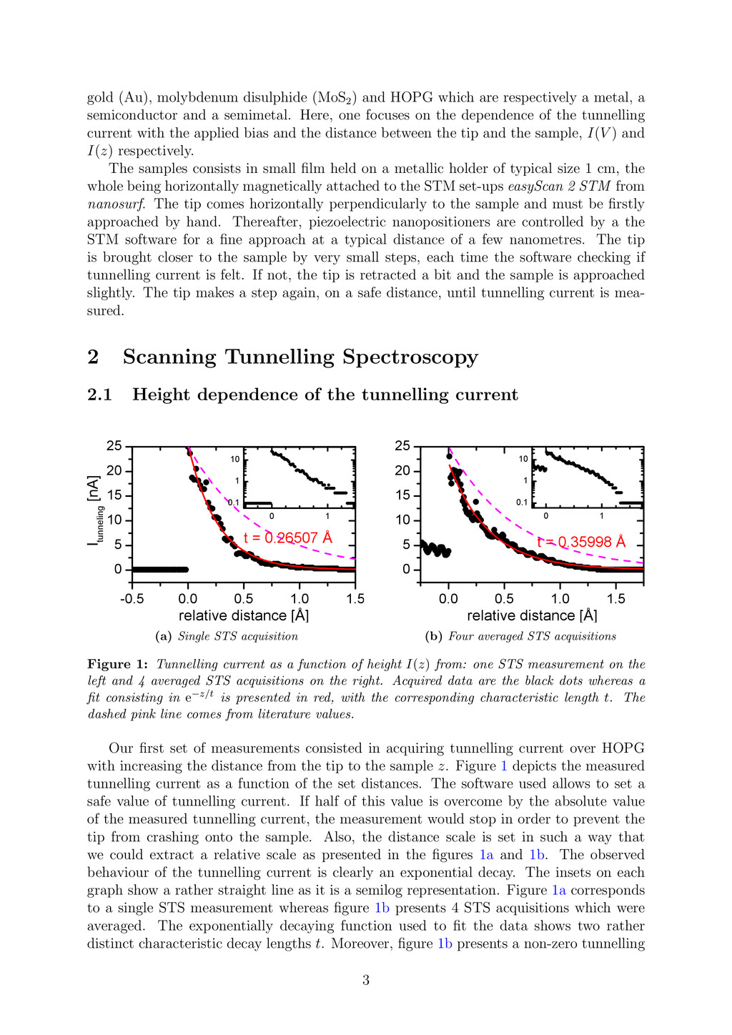
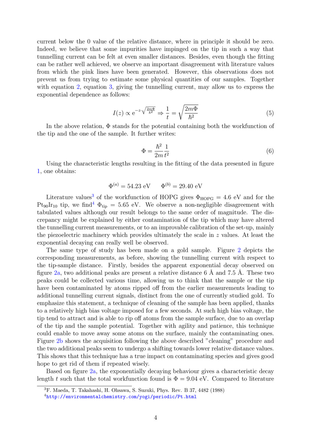
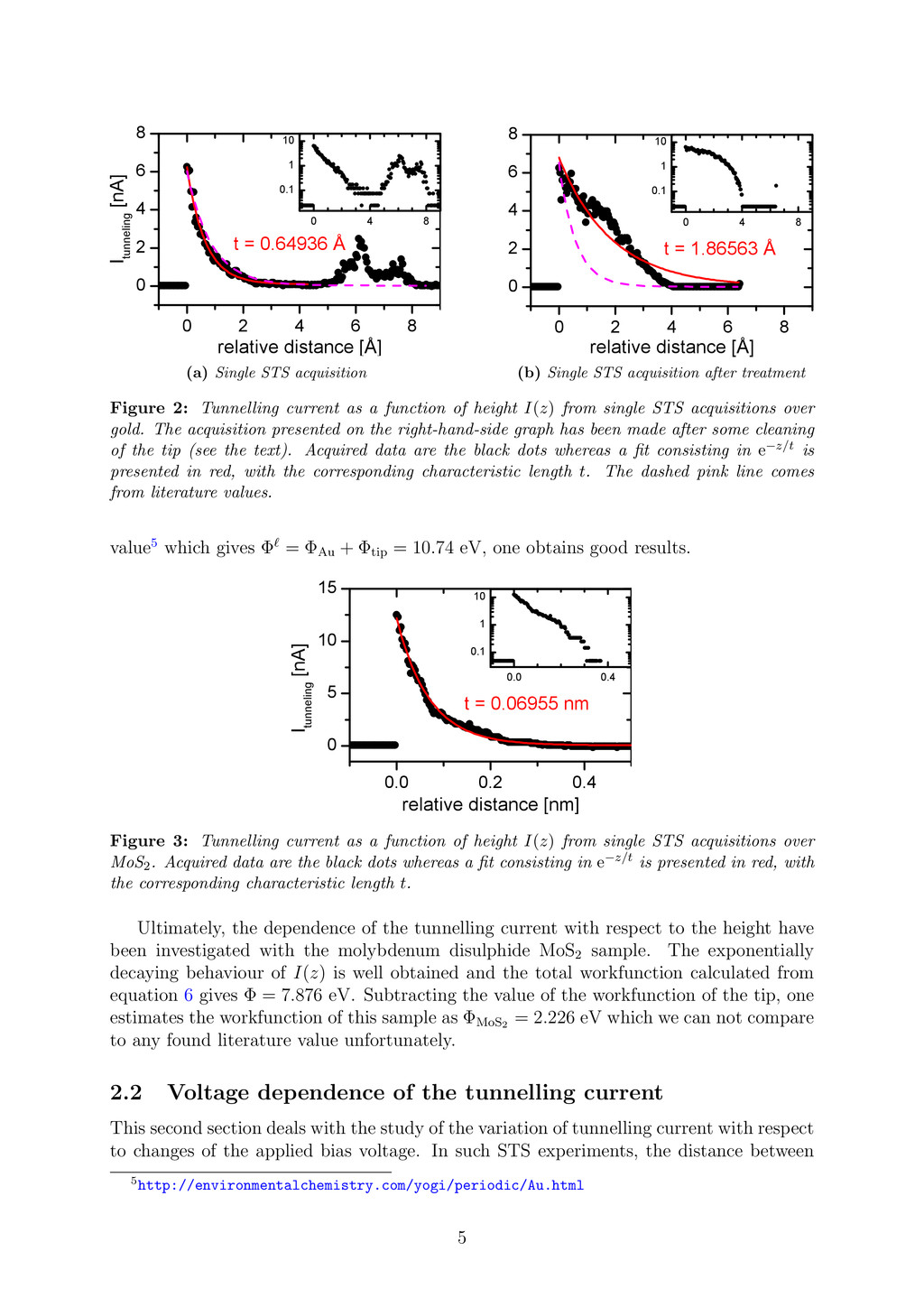
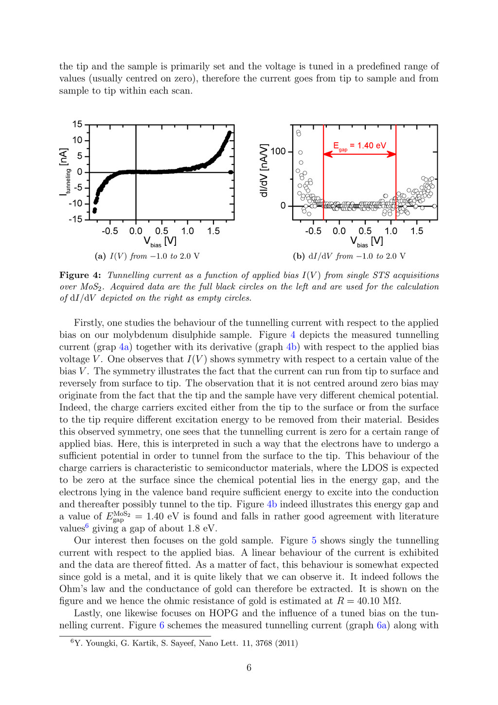
in principle it should be zero. Indeed, we believe that some impurities have impinged on the tip in such a way that tunnelling current can be felt at even smaller distances. Besides, even though the fitting can be rather well achieved, we observe an important disagreement with literature values from which the pink lines have been generated. However, this observations does not prevent us from trying to estimate some physical quantities of our samples. Together with equation 2, equation 3, giving the tunnelling current, may allow us to express the exponential dependence as follows: I(z) ∝ e−z· 2mΦ 2 ⇒ 1 t = 2mΦ 2 (5) In the above relation, Φ stands for the potential containing both the workfunction of the tip and the one of the sample. It further writes: Φ = 2 2m 1 t2 (6) Using the characteristic lengths resulting in the fitting of the data presented in figure 1, one obtains: Φ(a) = 54.23 eV Φ(b) = 29.40 eV Literature values3 of the workfunction of HOPG gives ΦHOPG = 4.6 eV and for the Pt90 Ir10 tip, we find4 Φtip = 5.65 eV. We observe a non-negligible disagreement with tabulated values although our result belongs to the same order of magnitude. The dis- crepancy might be explained by either contamination of the tip which may have altered the tunnelling current measurements, or to an improvable calibration of the set-up, mainly the piezoelectric machinery which provides ultimately the scale in z values. At least the exponential decaying can really well be observed. The same type of study has been made on a gold sample. Figure 2 depicts the corresponding measurements, as before, showing the tunnelling current with respect to the tip-sample distance. Firstly, besides the apparent exponential decay observed on figure 2a, two additional peaks are present a relative distance 6 ˚ A and 7.5 ˚ A. These two peaks could be collected various time, allowing us to think that the sample or the tip have been contaminated by atoms ripped off from the earlier measurements leading to additional tunnelling current signals, distinct from the one of currently studied gold. To emphasize this statement, a technique of cleaning of the sample has been applied, thanks to a relatively high bias voltage imposed for a few seconds. At such high bias voltage, the tip tend to attract and is able to rip off atoms from the sample surface, due to an overlap of the tip and the sample potential. Together with agility and patience, this technique could enable to move away some atoms on the surface, mainly the contaminating ones. Figure 2b shows the acquisition following the above described ”cleaning” procedure and the two additional peaks seem to undergo a shifting towards lower relative distance values. This shows that this technique has a true impact on contaminating species and gives good hope to get rid of them if repeated wisely. Based on figure 2a, the exponentially decaying behaviour gives a characteristic decay length t such that the total workfunction found is Φ = 9.04 eV. Compared to literature 3F. Maeda, T. Takahashi, H. Ohsawa, S. Suzuki, Phys. Rev. B 37, 4482 (1988) 4http://environmentalchemistry.com/yogi/periodic/Pt.html 4
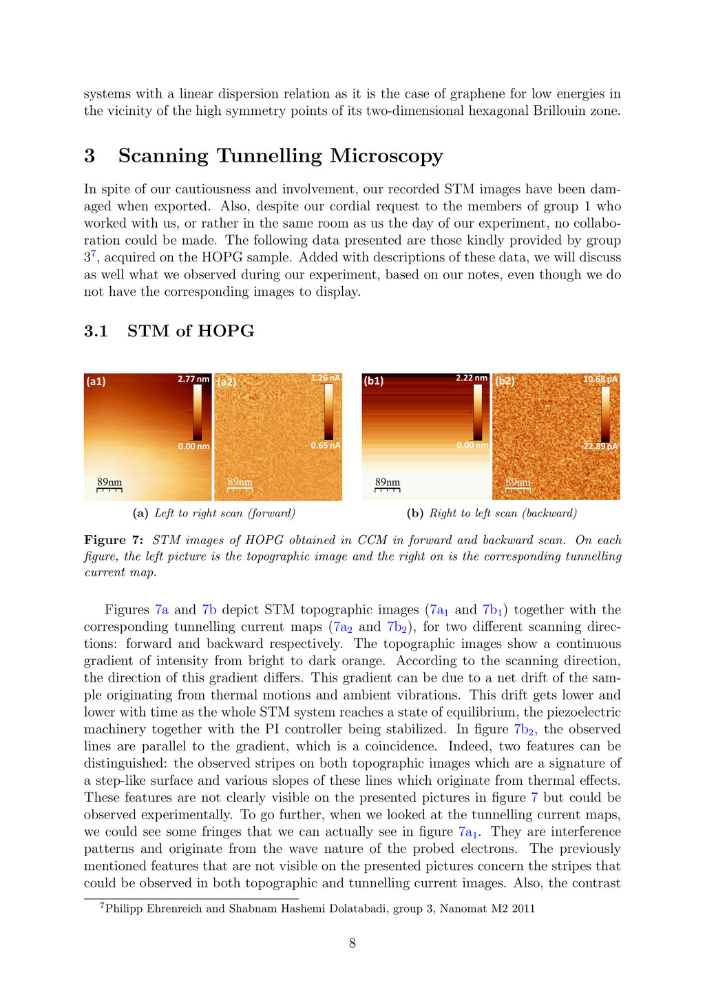
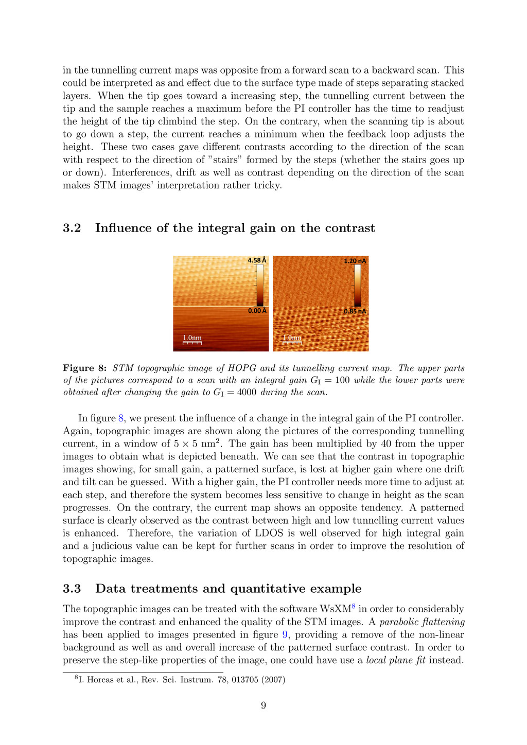
![-0.05 0.00 0.05 0.10 -2 0 2 I tunneling [nA]](https://files.speakerdeck.com/presentations/508a7fb6779e23000203135c/slide_8.jpg)
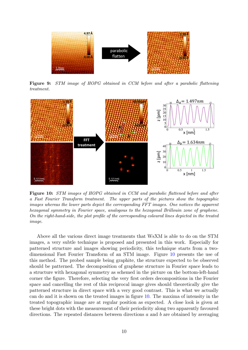
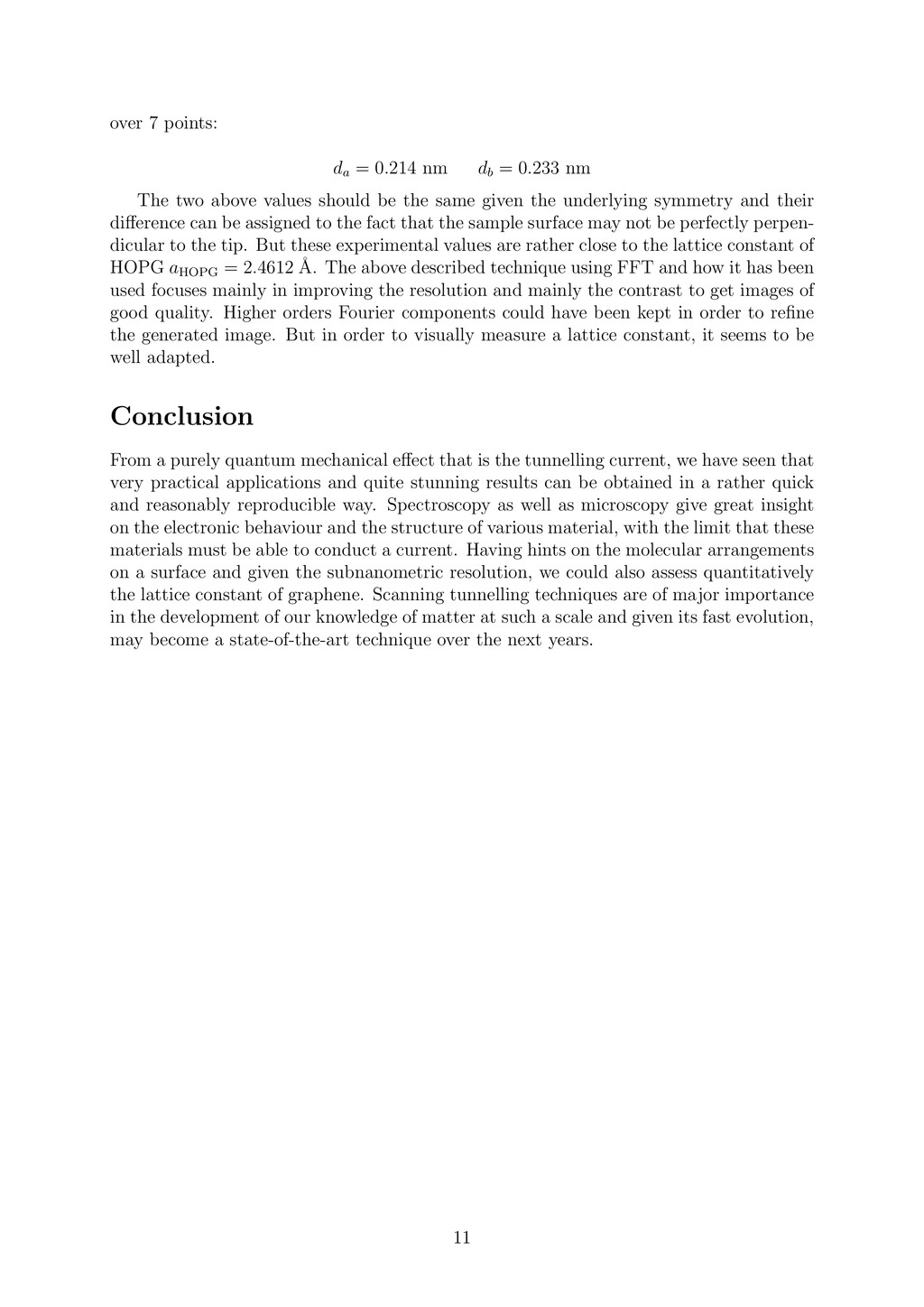