Upgrade to Pro — share decks privately, control downloads, hide ads and more …

Photoluminescence of semiconductor nanostructures - Master 2 SMNO Nanomat

jelledionot
November 01, 2011

Photoluminescence of semiconductor nanostructures - Master 2 SMNO Nanomat

jelledionot

November 01, 2011
Tweet

More Decks by jelledionot

Other Decks in Education

Transcript

  1. Nanomat NP428 – Functional Materials Practical 1 Photoluminescence of semiconductor

    nanostructures Universit´ e Pierre et Marie Curie Institut des Nanosciences de Paris Jelle Dionot
  2. Contents 1 Theoretical overview of photoluminescence 3 1.1 From spontaneous

    emission to photoluminescence . . . . . . . . . . . . . . . . . 3 1.2 From infinite potential well to real quantum well . . . . . . . . . . . . . . . . . 3 1.3 Transition energy in real heterostructures . . . . . . . . . . . . . . . . . . . . . 5 2 Experimental aspects 7 2.1 Experimental set-up . . . . . . . . . . . . . . . . . . . . . . . . . . . . . . . . . 7 2.1.1 Cryogenic conditions: the cryostat . . . . . . . . . . . . . . . . . . . . . 7 2.1.2 Exciting and emitted light: optical set-up . . . . . . . . . . . . . . . . . 7 2.2 Description of the samples . . . . . . . . . . . . . . . . . . . . . . . . . . . . . . 7 3 Measurements and calculations 10 3.1 C4H12: two thick quantum wells . . . . . . . . . . . . . . . . . . . . . . . . . . 10 3.2 Sample J211: single quantum well . . . . . . . . . . . . . . . . . . . . . . . . . 11 3.3 Sample NM133: quantum dots . . . . . . . . . . . . . . . . . . . . . . . . . . . 12 A Resolution of the implicit equation of confined states’ energy 15 1
  3. Introduction The photoluminescence spectroscopy allows to probe solids optical transitions

    thanks to an exciting light source and to the measure of the emitted light resulting from the recombination of excited electrons. It is widely used namely to measure the purity and crystalline quality of semiconductor materials, as well as to identify surface and interface and gauge alloy disorder and interface roughness. Also, information on the electronic bands structure and the SC energy gap can be obtained, as well as thermodynamics quantities such as temperature. A time resolved PL spectroscopy can also be done, giving rise to information about the dynamics of the carriers, allowing to measure the lifetime of the relaxations processes and excited states. The resolution of PL spectra is enhanced when in cryogenic conditions. Indeed, ther- mal excitation is lowered and therefore the energy of the excited carriers is less exposed to fluctuations due to thermal vibrations. The aim of this project is to compare the photoluminescence properties of a bulk semicon- ductor, semiconductor quantum wells – which present two-dimensional quantum confinement of electrons and holes – and semiconductor quantum wires with two-dimensional confinement. After a presentation of the experimental aspects of the practical, collected photoluminescence spectra from three SC samples are presented and commented in terms of emission wavelength (photon energy) and spectral characteristics (intensity, linewidth). These measurements are compared with calculations of the quantum confined energy levels and the expected emission energy from the transitions. 2
  4. Chapter 1 Theoretical overview of photoluminescence 1.1 From spontaneous emission

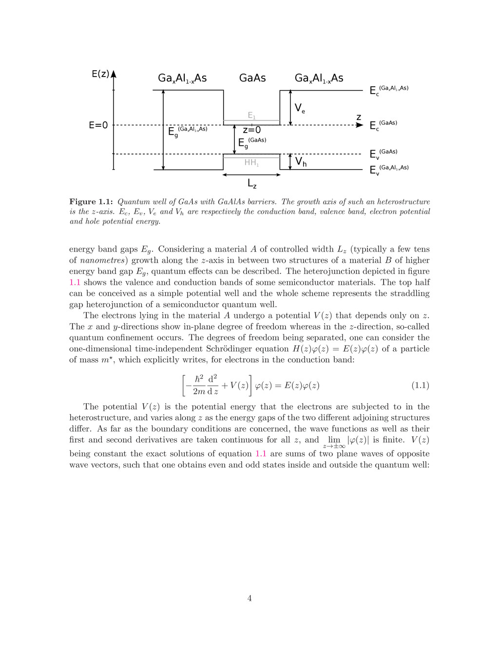
    to photoluminescence In atomic systems, the electrons lie in quantised states with various possible energies. Shining light on such systems can bring an electron, by the absorption of a photon, from an initial state to a final excited state higher in energy. The process of spontaneous emission then follows, in which the electron reaches back its initial state, emitting a photon of energy equal to the difference in energy of initial and final states. Solid state matter undergoes the same kind of transitions. When a solid is excited by a photon, two successive processes are involved: absorption and most likely photoluminescence. In the absorption process, the exciting light transfers its energy (and momentum) to matter in terms of creation of an electron-hole pair in the case of semiconductor (SC) materials. The study of the transmitted light – that is the fraction of light which remains after the absorption process – gives information on the sample, in terms of energy gap, electronic bands structure and density of states for low-dimensional systems for example. Also, excitonic effects can be observed since the exciting light can transfer energy (i.e. be absorbed) to available excitonic states. The subsequent photoluminescence process occurs when the induced electron-hole pair relaxes. The emitted light energy is characteristic of the solid structure it comes from. In the case of SC structures and heterostructures, the radiative recombination of the charge carriers follows the non-radiative relaxation process that brings the electron and holes to the bottom and top of the conduction and valence band respectively. Moreover, the actual radiative recombination starts from the lowest lying state for the electron-hole pair, that is the lowest available excitonic state. This is to be compared with absorption experiment and the qualitative and quantitative differences in information both techniques give access to, besides their difference in terms of experimental requisites and aspects. 1.2 From infinite potential well to real quantum well Semiconductor materials can be growth either as bulk structures or as superposition of lay- ers of various compositions. The different semiconductor alloys have different characteristic 3
  5. Ga x Al 1-x As Ga x Al 1-x As

    GaAs E(z) E g (GaAs) E=0 E g (Ga x Al 1-x As) E c (Ga x Al 1-x As) E v (Ga x Al 1-x As) E c (GaAs) E v (GaAs) V e Vh Lz z z=0 E1 HH 1 Figure 1.1: Quantum well of GaAs with GaAlAs barriers. The growth axis of such an heterostructure is the z-axis. Ec , Ev , Ve and Vh are respectively the conduction band, valence band, electron potential and hole potential energy. energy band gaps Eg. Considering a material A of controlled width Lz (typically a few tens of nanometres) growth along the z-axis in between two structures of a material B of higher energy band gap Eg, quantum effects can be described. The heterojunction depicted in figure 1.1 shows the valence and conduction bands of some semiconductor materials. The top half can be conceived as a simple potential well and the whole scheme represents the straddling gap heterojunction of a semiconductor quantum well. The electrons lying in the material A undergo a potential V (z) that depends only on z. The x and y-directions show in-plane degree of freedom whereas in the z-direction, so-called quantum confinement occurs. The degrees of freedom being separated, one can consider the one-dimensional time-independent Schr¨ odinger equation H(z)ϕ(z) = E(z)ϕ(z) of a particle of mass m⋆, which explicitly writes, for electrons in the conduction band: − 2 2m d2 d z + V (z) ϕ(z) = E(z)ϕ(z) (1.1) The potential V (z) is the potential energy that the electrons are subjected to in the heterostructure, and varies along z as the energy gaps of the two different adjoining structures differ. As far as the boundary conditions are concerned, the wave functions as well as their first and second derivatives are taken continuous for all z, and lim z→±∞ |ϕ(z)| is finite. V (z) being constant the exact solutions of equation 1.1 are sums of two plane waves of opposite wave vectors, such that one obtains even and odd states inside and outside the quantum well: 4
  6. ϕA(z) =    A cos (kAz) for even

    states A sin (kAz) for odd states for |z| ≤ Lz/2 ϕB(z) =    BekB (z−Lz/2) + Ce−kB (z−Lz/2) for z > Lz/2 DekB (z+Lz/2) + Ee−kB (z+Lz/2) for z < −Lz/2 with    kA = 2m⋆ A E ¯ h2 kB = 2m⋆ B 2 (V (z) − E) (1.2) One notes that since |ϕ(z)| should not diverge when z → ±∞, C = D = 0, and for even states, B = −E and for odd states B = E. Applying the boundary conditions at the interfaces z = ±Lz/2, the energy of the bound states satisfies the following implicit equations:        cos kA LA 2 = m⋆ B m⋆ A kA kB sin kA LA 2 even cos kA LA 2 = −m⋆ A m⋆ B kB kA sin kA LA 2 odd (1.3) The case of an infinite quantum well is obtained in the limit V (z) → ∞, which implies ϕ(|z| = Lz 2 ) = 0. The discrete values of kA are in that case given by kALz = pπ (p ∈ N). The quantized energy in an infinite quantum well hence reads: Ep = 2k2 A 2m⋆ = p 2π2 2m⋆L2 z (1.4) Therefore the energy is inversely proportional to the effective mass and to the square of the well thickness Lz. The resolution of equation 1.3 consists in finding the energy value E for which the left- hand-side (LHS) and the right-hand-side (RHS) are verified. A MATLAB code presented in appendix A on page 15 is devoted to this and yields the energy value of the first quantized state for and electron and for a hole for the two sampled quantum well heterostructures C4H12 and J211 (see sections 3.1 and 3.2 starting on page 10). 1.3 Transition energy in real heterostructures The couple of equations 1.3 holds also for holes in the valence band. These equations are solved numerically and used in the following within chapter 3 starting on page 10 for the calculation of confinement energies of electrons and holes, in a view to calculating the band- to-band transition energy of photoluminescence processes. Since the radiative relaxation of PL processes occur only after non-radiative processes which occur faster, one will focus on the lowest transitions, that is to say of smallest energy. Knowing that the valence band is made of one heavy-hole band and one light-hole band (neglecting the underlying spin-orbit 5
  7. GaAs Ga1−xAlxAs AlAs Eg 1.519 + 1.3668x + 0.2211x2 m⋆

    e 0.067 0.067(1 − x) + 0.13x 0.13 m⋆ h 0.38 0.38(1 − x) + 0.46x 0.46 Table 1.1: Energy gap and effective masses for GaAs and AlAs and intermediate alloy Ga1−x Alx As. band), and that the effective mass of the light-holes is larger than the one of the heavy-hole, one will focus on the transitions between the lowest lying electrons in the conduction band holes of the heavy-hole band. Therefore, the confinement energies derived from the resolution of equations 1.3 will be E1 and HH1. The confined electrons and holes being charged particles, they interact together through Coulomb forces. Such interactions give rise to a relative stabilization of these particles in their respective bands, in a bound state called exciton. This quasi-particle have a binding energy Eexc. The transition energy of the PL process being the relaxation of the electron-hole pair (E1, HH1) within the band gap (Egap), against the corresponding excitonic binding energy (Eexc), it hence reads: Etrans = Egap + E1 + HH1 − Eexc (1.5) Other phenomena such as lattice vibrations occur and affect the transition energy but they can be reasonably neglected at cryogenic temperatures. The transition energy of the photon emitted during a PL process can thus be calculated from the knowledge of the energy band gap, the confinement energies and if necessary the exciton binding energy. The prerequisites in use for the following work in which one consider GaAs and Ga1−xAlxAs compounds are summed up in table 1.1. 6
  8. Chapter 2 Experimental aspects 2.1 Experimental set-up The sample are

    held in a cryostat and excited by a Helium-Neon laser. The emitted light is then captured by an optical fibre plugged to a spectrometer. 2.1.1 Cryogenic conditions: the cryostat As mentioned previously, in order to avoid interaction between charge carriers and thermally excited phonons, the sample are cooled to cryogenic temperatures, at around 2 K. The samples are held in a cryostat which is depicted in figure 2.1. It consists in two main baths separated by a vacuum tank. The outermost bath is filled with liquid Nitrogen at 77 K. The three samples are maintained by a rotatable holder and immersed in the inner bath which contains liquid Helium at around 4 K. This last boils at 4.2 K, therefore the temperature needs to be even lower to avoid bubbles that can cause light to scatter. Hence the inner part of the cryostat is pumped and the pressure is decreased as well as the temperature, which reaches 2 K. At such a temperature, Helium reaches superfluid phase which ensures no parasitic light scattering. 2.1.2 Exciting and emitted light: optical set-up The photoluminescence experiment requires an exciting light source as well as a spectrometer, the whole finely adjusted by a set of optical devices such as lenses and polariser. The optical set-up is shown in figure 2.2 and consists in a Helium-Neon laser of wavelength λ = 623.8 nm whose beam is focused by a lens of focal 400 mm onto the selected sample, shining the sample on locally around 100 ñm2. The light from the photoluminescence process is then focused by a lens of focal 240 mm onto an optical fibre. One has first taken precautions of not aligning any reflected light on the collecting lens. The optical fibre is plugged to a spectrometer equipped with a CCD detector, driven by a computer allowing us to acquire data. 2.2 Description of the samples The samples studied during the experiment were of three types. Two quantum well (QWL) structures and one quantum wire (QWR) with self assembled quantum dots (QDs) all along. 7
  9. (a) Photograph (b) Scheme Figure 2.1: Photograph of the cryostat

    and a corresponding scheme. The cryostat is approximately 1 meter high and the distances are given indicatively in centimetres in the schematic picture. Specular reflection Photoluminescence light (in dashed lines) Cryostat Samples Focusing lenses He-Ne laser Optical fibre Grating Spectrometer CCD Camera Computer Figure 2.2: Optical set-up from the exciting light source to the analysing computer-driven spectrome- ter. The optical fibre is plugged to a spectrometer which measures light intensity at different wavelength, thanks to a CCD camera whose collected signal is monitored on the computer. 8
  10. The sample C4H12 contains two thick GaAs quantum wells of

    length L = 84.16 ˚ A separated by – and placed side by side to – AlAs layers of approximately 10 nm thickness. The sample J211 presents a thin GaAs QWL of length L = 10 ˚ A in between two Ga0.7Al0.3As layers. The sample NM133 consists in a collection of GaAs quantum dots (QDs) formed along the free axis of a 10 nm thick quantum wire (QWR), due to the interface thickness fluctuations of ± 1 monolayer (ML) during the epitaxy of the GaAs structure in the V-groove GaAl0.3As structure. 9
  11. Chapter 3 Measurements and calculations 3.1 C4H12: two thick quantum

    wells The first measurements were done on the C4H12 sample and the corresponding PL spectrum is depicted in figure 3.1. The main peak at λ = 789.38 nm is the actual PL response of one of the quantum well contained in the sample, but the small peak at lower energy (i.e. higher wavelength) does not correspond to a second quantum well PL response. It is too narrow to be compared to the main peak, given the structural similarities of the quantum wells. A detection at other ranges of wavelength could have let us observe the spectral response of the second quantum well. Hence the experimental transition energy measured from photoluminescence for sample C4H12 is Etrans = 1.571 eV. 0.2 0.3 0.4 0.5 0.6 0.7 0.8 0.9 1 782 784 786 788 790 792 794 796 798 Intensity (normalized) Wavelength (nm) data 1.5706 eV Figure 3.1: Photoluminescence spectrum of C4H12 sample. Exposure time 1 second, detection wave- length 790 ± 8 nm. The maximum of PL intensity is reached for λ = 789.38 nm that is 1.5706 eV. This experimental value is compared to the calculation of the transition energy given in equation 1.5 of section 1.3 on page 5. The energy gap is given by the table 1.1 and the 10
  12. confinement energies of the electron-hole pair computed from the implicit

    equation 1.3. The MATLAB code elaborated for this graphical resolution is given in appendix A on page A. -0.4 -0.2 0 0.2 0.4 0.6 0.8 1 0 0.02 0.04 0.06 0.08 0.1 Electron confinement energy (eV) LHS RHS (a) Electron -1 -0.8 -0.6 -0.4 -0.2 0 0.2 0.4 0.6 0.8 1 0 0.01 0.02 0.03 0.04 0.05 Hole confinement energy (eV) LHS RHS (b) Hole Figure 3.2: Plot representing the crossing of RHS and LHS of equation 1.3 as a function of energy, for electrons (a) and holes (b) of sample C4H12. Figure 3.2 shows the energy that satisfies the implicit equation mentioned above. The obtained electron and hole confinement energies for C4H12 are respectively E1 = 49.1 meV and HH1 = 10.7 meV. This gives a calculated transition energy of order: Ecalc trans = 1.519 + 0.049 + 0.011 ≃ 1.579 eV The energy difference between experiment and calculation is therefore δE ≃ 8 meV which can originate from the exciton binding energy (for at least 4 meV given its bulk value), phonon interactions (although minimized by the cryogenic temperature), or even experimental artefacts from the spectrometer. 3.2 Sample J211: single quantum well The second set of measurements is related to the study of sample J211 which consists in a single GaAs quantum well of length Lz = 10 ˚ A. The photoluminescence spectra is presented in 3.3. The main PL peak shows a transition energy Etrans = 1.894 eV. Likewise, the calculation of the expected transition energy is obtained thanks to the energy of the lowest confined states, graphically depicted in 3.4. The obtained electron and hole confinement energies for J211 are respectively E1 = 0.235 eV and HH1 = 0.104 eV. Together with the calculated energy gap, one obtains the transition energy: Ecalc trans = 1.519 + 0.235 + 0.104 ≃ 1.858 eV Compared to the experimental value, the energy difference is ∆E ≃ 36 meV. Apparently, the difference here is much more important. Also, one can see that the PL response for sample 11
  13. 0.1 0.2 0.3 0.4 0.5 0.6 0.7 0.8 0.9 1

    648 650 652 654 656 658 660 662 Intensity (normalized) Wavelength (nm) data Figure 3.3: Photoluminescence spectrum of J211 sample. Exposure time 1 second, detection wave- length 655 ± 7 nm. The maximum of PL intensity is reached for λ = 654.63 nm that is 1.8939 eV. J211 is much broader, which suggests a much smaller excited states lifetime. Besides, the Gaussian look of this photoluminescence line reveals some dependency to randomly distributed variables such as thickness fluctuation or impurities. Added to an apparent shift in energy (∆E), the calculation here shows less agreement with the data, even though systematic errors and inaccuracy from the set-up may still be taken into account. 3.3 Sample NM133: quantum dots The last sample of this series of PL experiment contains randomly distributed GaAs quantum dots along a quantum wire structure. Its PL line is proposed in figure 3.5. The maximum is reached at an energy Etrans = 1.626 eV. The data treatment has exhibited a better fit when two Gaussian curves were used (instead of one). Indeed, the whole line shows asymmetry with respect to its maximum, where it goes down to its minimum slower at higher wavelength, that is at lower energy. When this ’shoulder’ at higher wavelength is taken into account for the fitting, best matching is obtained. Fundamentally, the laser source excites thousands of quantum dots and the PL response is indeed the sum of all the self assembled QDs of various size in the QWR. The laser spot is approximately 100 µm2 and there are 1010 − 1012 QDs.cm−2, and: 100 µm2 = 10−8 cm2 that is the excitation of at least 103 quantum dots. Coupled with this great amount of different excitations, localized excitons can form and lead to this homogeneous shifting in energy. 12
  14. 0 0.5 1 1.5 2 2.5 3 3.5 0 0.05

    0.1 0.15 0.2 0.25 0.3 Electron confinement energy (eV) LHS RHS (a) Electron 0 1 2 3 4 5 0 0.05 0.1 0.15 Hole confinement energy (eV) LHS RHS (b) Hole Figure 3.4: Plot representing the RHS and LHS of equation 1.3 as a function of energy, for electron confinement energy (a) and hole confinement energy (b) of sample J211. 0 0.1 0.2 0.3 0.4 0.5 0.6 0.7 0.8 0.9 1 1.1 756 758 760 762 764 766 768 770 Intensity (normalized) Wavelength (nm) data fit Figure 3.5: Photoluminescence spectrum of J211 sample. Exposure time 1 second, detection wave- length 763 ± 7 nm. The maximum of PL intensity is reached for λ = 762.52 nm that is 1.6259 eV. 13
  15. Conclusion In the first practical of the Functional Materials course

    NP428, an experiment of photolu- minescence from semiconductor heterostructures has been held, from which emission energy spectra were measured and compared with analytical calculations and the resulting expected emission energy. The corresponding experimental as well as theoretical aspects were covered. The experimental procedures are not extremely demanding except maybe for the required cryogenic temperatures; the rest of the PL set-up consisting essentially in a laser, two lenses and quite of a simple acquiring machinery. Together with relatively simple theoretical mod- els, photoluminescence experiment allows to collect numerous information about the lowest band-to-band transitions in semiconductor materials. The last sample in study consisted in quantum dots that couldn’t be resolved individually. A further study, higher resolved, such as microphotoluminescence experiments, in which the laser source is much more focused on the sample in order to probe a single quantum dot, would essentially give deeper insights of such low-dimensional materials. 14
  16. Appendix A Resolution of the implicit equation of confined states’

    energy This section presents the MATLAB code used to solve the equation 1.3 on page 5. The output values were actually exported and GNUplot was used to yield the plots. x = 1; h = 0; % h = 0, calculation for electron, h = 1 for hole ML = 0 Eg = 1.519 + 1.3668*x + 0.2211*x^2; Eg = Eg*1.618e-19; % band gap in Joule for SI calculations E = 0:0.0001:0.14; % range from 0 to 0.1 eV E = E*1.618e-19; % energy in Joule for homogeneity hbar = 1.05457148e-34; % SI me = 9.10938188e-31; % SI Voff = ((1-h)*(2/3) + h*(1/3))*(Eg-1.519*1.618e-19); mGaAs = (1-h)*0.067*me+h*0.38*me; mAlAs = (1-h)*0.13*me+h*0.46*me; mGaAlAs = x*mAlAs+(1-x)*mGaAs; LGaAs = (86.21+2.83*ML)*1e-10; for i = 1:length(E) kGaAs(i) = sqrt( (2*mGaAs*E(i))/(hbar^2) ); kAlAs(i) = sqrt( (2*mAlAs*(Voff - E(i)))/(hbar^2) ); kGaAlAs(i) = sqrt( (2*mGaAlAs*(Voff - E(i)))/(hbar^2) ); left(i) = cos((kGaAs(i)*LGaAs)/2); right(i) = (mAlAs/mGaAs)*(kGaAs(i)/kAlAs(i))*sin((kGaAs(i)*LGaAs)/2); end plot(E,left);hold on;plot(E,right) 15
  17. 16